NB100LVEP221
2.5V/3.3V 2:1:20
Differential HSTL/ECL/PECL
Clock Driver
Description
The NB100LVEP221 is a low skew 2:1:20 differential clock driver,
designed with clock distribution in mind, accepting two clock sources
into an input multiplexer. The two clock inputs are differential
ECL/PECL; CLK1/CLK1 can also receive HSTL signal levels. The
LVPECL input signals can be either differential configuration or
single−ended (if the VBB output is used).
The LVEP221 specifically guarantees low output−to−output skew.
Optimal design, layout, and processing minimize skew within a device
and from device to device.
To ensure tightest skew, both sides of differential outputs should be
terminated identically into 50 W even if only one output is being used.
If an output pair is unused, both outputs may be left open
(unterminated) without affecting skew.
The NB100LVEP221, as with most other ECL devices, can be
operated from a positive VCC supply in LVPECL mode. This allows the
LVEP221 to be used for high performance clock distribution in +3.3 V or
+2.5 V systems. In a PECL environment, series or Thevenin line
terminations are typically used as they require no additional power
supplies. For more information on PECL terminations, designers should
refer to Application Note AND8020/D.
The VBB pin, an internally generated voltage supply, is available to this
device only. For single−ended LVPECL input conditions, the unused
differential input is connected to VBB as a switching reference voltage.
VBB may also rebias AC coupled inputs. When used, decouple VBB and
VCC via a 0.01 mF capacitor and limit current sourcing or sinking to
0.5 mA. When not used, VBB should be left open.
Single−ended CLK input operation is limited to a VCC ≥ 3.0 V in
LVPECL mode, or VEE ≤ −3.0 V in NECL mode.
www.onsemi.com
MARKING
DIAGRAM*
52
1
1
NB100
LVEP221
AWLYYWWG
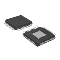
52
QFN52
MN SUFFIX
CASE 485M
A
WL
YY
WW
G
= Assembly Location
= Wafer Lot
= Year
= Work Week
= Pb−Free Package
*For additional marking information, refer to
Application Note AND8002/D.
ORDERING INFORMATION
See detailed ordering and shipping information in the package
dimensions section on page 8 of this data sheet.
Features
•
•
•
•
•
•
•
•
•
•
•
•
15 ps Typical Output−to−Output Skew
40 ps Typical Device−to−Device Skew
Jitter Less than 2 ps RMS
Maximum Frequency > 1.0 GHz Typical
Thermally Enhanced 52−Lead QFN Package
VBB Output
540 ps Typical Propagation Delay
LVPECL and HSTL Mode Operating Range:
VCC = 2.375 V to 3.8 V with VEE = 0 V
NECL Mode Operating Range:
VCC = 0 V with VEE = −2.375 V to −3.8 V
Q Output will Default Low with Inputs Open or at VEE
Pin Compatible with Motorola MC100EP221
These Devices are Pb−Free and are RoHS Compliant
© Semiconductor Components Industries, LLC, 2015
January, 2019 − Rev. 11
1
Publication Order Number:
NB100LVEP221/D
�Q1
Q2
Q2
Q
3
Q3
Q4
Q4
Q5
Q5
VCC0
49
48
47
46
44
43
42
41
40
45
Q1
50
51
Q
0
Q0
52
NB100LVEP221
Exposed Pad (EP)
VCC0
1
39
Q6
VCC
2
38
Q6
CLKSEL
3
37
Q7
CLK0
4
36
Q7
CLK0
5
35
Q8
VBB
6
34
Q8
CLK1
7
33
Q9
CLK1
8
32
Q9
VEE
9
31
Q10
Q19
10
30
Q10
Q19
11
29
Q11
Q18
12
28
Q11
Q18
13
27
VCC0
24
25
26
Q12
Q12
21
Q14
Q13
20
Q15
23
19
Q15
Q13
18
Q16
22
17
Q16
Q14
16
Q17
15
Q17
VCC0
14
NB100LVEP221
Figure 1. 52−Lead QFN Pinout (Top View)
Table 1. PIN DESCRIPTION
PIN
FUNCTION
CLK0*, CLK0**
ECL/PECL Differential Inputs
CLK1*, CLK1**
ECL/PECL or HSTL Differential Inputs
Q0:19, Q0:19
ECL/PECL Differential Outputs
CLK_SEL*
ECL/PECL Active Clock Select Input
VBB
Reference Voltage Output
VCC/VCCO
Positive Supply
VEE***
Negative Supply
CLK0
0
CLK0
20
CLK1
20
1
CLK1
* Pins will default LOW when left open.
** Pins will default HIGH when left open.
*** The thermally conductive exposed pad on the bottom of the
package is electrically connected to VEE internally.
VBB
CLK_SEL
VCC
Table 2. FUNCTION TABLE
VEE
CLK_SEL
Active Input
L
H
CLK0, CLK0
CLK1, CLK1
Figure 2. Logic Diagram
www.onsemi.com
2
Q0 − Q19
Q0 − Q19
�NB100LVEP221
Table 3. ATTRIBUTES
Characteristics
Value
Internal Input Pulldown Resistor
75 kW
Internal Input Pullup Resistor
37.5 kW
ESD Protection
Human Body Model
Machine Model
Charged Device Model
Moisture Sensitivity, Indefinite Time Out of Drypack (Note 1)
QFN52
Flammability Rating
Oxygen Index: 28 to 34
Transistor Count
> 2 kV
> 200 V
> 2 kV
Pb−Free Pkg
Level 2
UL 94 V−0 @ 0.125 in
533 Devices
Meets or exceeds JEDEC Spec EIA/JESD78 IC Latchup Test
1. For additional information, refer to Application Note AND8003/D.
Table 4. MAXIMUM RATINGS
Symbol
Parameter
Condition 1
Condition 2
Rating
Unit
VCC
PECL Mode Power Supply
VEE = 0 V
6
V
VEE
NECL Mode Power Supply
VCC = 0 V
−6
V
VI
PECL Mode Input Voltage
NECL Mode Input Voltage
VEE = 0 V
VCC = 0 V
6
−6
V
V
Iout
Output Current
Continuous
Surge
50
100
mA
mA
IBB
VBB Sink/Source
± 0.5
mA
TA
Operating Temperature Range
−40 to +85
°C
Tstg
Storage Temperature Range
−65 to +150
°C
qJA
Thermal Resistance (Junction−to−Ambient)
(Note )
0 lfpm
500 lfpm
QFN52
QFN52
25
19.6
°C/W
°C/W
qJC
Thermal Resistance (Junction−to−Case) (Note )
2S2P
QFN52
21
°C/W
Tsol
Wave Solder
265
265
°C
Pb
Pb−Free
VI ≤ VCC
VI ≥ VEE
Stresses exceeding those listed in the Maximum Ratings table may damage the device. If any of these limits are exceeded, device functionality
should not be assumed, damage may occur and reliability may be affected.
www.onsemi.com
3
�NB100LVEP221
Table 5. LVPECL DC CHARACTERISTICS VCC = 2.5 V; VEE = 0 V (Note 2)
−40°C
Symbol
Characteristic
25°C
85°C
Min
Typ
Max
Min
Typ
Max
Min
Typ
Max
Unit
IEE
Power Supply Current
100
125
150
104
130
156
116
145
174
mA
VOH
Output HIGH Voltage (Note 3)
1355
1480
1605
1355
1480
1605
1355
1480
1605
mV
VOL
Output LOW Voltage (Note 3)
555
680
900
555
680
900
555
680
900
mV
VIH
Input HIGH Voltage (Single−Ended) (Note 4)
1335
1620
1335
1620
1275
1620
mV
VIL
Input LOW Voltage (Single−Ended) (Note 4)
555
900
555
900
555
900
mV
VIHCMR
Input HIGH Voltage Common Mode Range
(Differential Configuration) (Note 5)
CLK0/CLK0
CLK1/CLK1
1.2
0.3
2.5
1.6
1.2
0.3
2.5
1.6
1.2
0.3
2.5
1.6
V
V
150
mA
IIH
Input HIGH Current
IIL
Input LOW Current
150
CLK
CLK
0.5
−150
150
0.5
−150
0.5
−150
mA
NOTE: Device will meet the specifications after thermal equilibrium has been established when mounted in a test socket or printed circuit
board with maintained transverse airflow greater than 500 lfpm.
2. Input and output parameters vary 1:1 with VCC. VEE can vary + 0.125 V to −1.3 V.
3. All outputs loaded with 50 W to VCC − 2.0 V.
4. Do not use VBB at VCC < 3.0 V.
5. VIHCMR min varies 1:1 with VEE, VIHCMR max varies 1:1 with VCC. The VIHCMR range is referenced to the most positive side of the differential input signal.
Table 6. LVPECL DC CHARACTERISTICS VCC = 3.3 V; VEE = 0 V (Note 6)
−40°C
25°C
85°C
Min
Typ
Max
Min
Typ
Max
Min
Typ
Max
Unit
IEE
Power Supply Current
100
125
150
104
130
156
116
145
174
mA
VOH
Output HIGH Voltage (Note 7)
2155
2280
2405
2155
2280
2405
2155
2280
2405
mV
VOL
Output LOW Voltage (Note 7)
1355
1480
1700
1355
1480
1700
1355
1480
1700
mV
VIH
Input HIGH Voltage (Single−Ended)
2135
2420
2135
2420
2135
2420
mV
VIL
Input LOW Voltage (Single−Ended)
1355
1700
1355
1700
1355
1700
mV
VBB
Output Reference Voltage (Note 8)
1775
1975
1775
1975
1775
1975
mV
VIHCMR
Input HIGH Voltage Common Mode Range
(Differential Configuration) (Note 9)
CLK0/CLK0
CLK1/CLK1
3.3
1.6
1.2
0.3
3.3
1.6
1.2
0.3
3.3
1.6
V
V
150
mA
Symbol
Characteristic
IIH
Input HIGH Current
IIL
Input LOW Current
1875
1.2
0.3
150
CLK
CLK
0.5
−150
1875
150
0.5
−150
0.5
−150
1875
mA
NOTE: Device will meet the specifications after thermal equilibrium has been established when mounted in a test socket or printed circuit
board with maintained transverse airflow greater than 500 lfpm.
6. Input and output parameters vary 1:1 with VCC. VEE can vary + 0.925 V to −0.5 V.
7. All outputs loaded with 50 W to VCC − 2.0 V.
8. Single−ended input operation is limited VCC ≥ 3.0 V in LVPECL mode.
9. VIHCMR min varies 1:1 with VEE, VIHCMR max varies 1:1 with VCC. The VIHCMR range is referenced to the most positive side of the differential
input signal.
www.onsemi.com
4
�NB100LVEP221
Table 7. LVNECL DC CHARACTERISTICS VCC = 0 V, VEE = −2.375 V to −3.8 V (Note 10)
−40°C
Symbol
Characteristic
25°C
85°C
Min
Typ
Max
Min
Typ
Max
Min
Typ
Max
Unit
100
125
150
104
130
156
116
145
174
mA
IEE
Power Supply Current
VOH
Output HIGH Voltage (Note 11)
−1145
−1020
−895
−1145
−1020
−895
−1145
−1020
−895
mV
VOL
Output LOW Voltage (Note 11)
−1945
−1820
−1600
−1945
−1820
−1600
−1945
−1820
−1600
mV
VIH
Input HIGH Voltage (Single−Ended)
−1165
−880
−1165
−880
−1165
−880
mV
VIL
Input LOW Voltage (Single−Ended)
−1945
−1600
−1945
−1600
−1945
−1600
mV
VBB
Output Reference Voltage (Note 12)
−1525
−1325
−1525
−1325
−1525
−1325
mV
VIHCMR
Input HIGH Voltage Common Mode
Range (Differential Configuration)
(Note 13)
CLK0/CLK0
CLK1/CLK1
0.0
−0.9
V
V
150
mA
IIH
Input HIGH Current
IIL
Input LOW Current
−1425
VEE + 1.2
VEE + 0.3
0.0
−0.9
−1425
VEE + 1.2
VEE + 0.3
150
CLK
CLK
0.0
−0.9
−1425
VEE + 1.2
VEE + 0.3
150
0.5
−150
0.5
−150
0.5
−150
mA
NOTE: Device will meet the specifications after thermal equilibrium has been established when mounted in a test socket or printed circuit
board with maintained transverse airflow greater than 500 lfpm.
10. Input and output parameters vary 1:1 with VCC.
11. All outputs loaded with 50 W to VCC−2.0 V.
12. Single−ended input operation is limited VEE ≤ −3.0V in NECL mode.
13. VIHCMR min varies 1:1 with VEE, VIHCMR max varies 1:1 with VCC. The VIHCMR range is referenced to the most positive side of the differential
input signal.
Table 8. HSTL DC CHARACTERISTICS VCC = 3.3 V; VEE = 0 V
0°C
Symbol
Min
Characteristic
VIH
Input HIGH Voltage
VIL
Input LOW Voltage
VX
Typ
25°C
Max
Min
Typ
85°C
Max
Min
Typ
Max
Unit
CLK1/CLK1
Vx+100
1600
Vx+100
1600
Vx+100
1600
mV
CLK1/CLK1
−300
Vx−100
−300
Vx−100
−300
Vx−100
mV
Differential Configuration Cross
Point Voltage
680
900
680
900
680
900
mV
IIH
Input HIGH Current
−150
150
−150
150
−150
150
mA
IIL
Input LOW Current
CLK1
CLK1
−150
−250
−150
−250
−150
−250
mA
NOTE: Device will meet the specifications after thermal equilibrium has been established when mounted in a test socket or printed circuit
board with maintained transverse airflow greater than 500 lfpm.
www.onsemi.com
5
�NB100LVEP221
Table 9. AC CHARACTERISTICS VCC = 0 V; VEE = −2.375 to −3.8 V or VCC = 2.375 to 3.8 V; VEE = 0 V (Note 14)
−40°C
Symbol
Characteristic
Min
Typ
550
550
500
700
700
700
25°C
Max
Min
Typ
600
550
500
700
700
700
85°C
Max
Min
Typ
600
500
400
700
700
600
Max
Unit
VOpp
Differential Output Voltage
(Figure 3)
tPLH/tPHL
Propagation Delay (Differential Configuration)
CLK0−Qx
CLK1−Qx
540
590
600
640
540
590
660
710
540
590
750
800
ps
ps
tskew
Within−Device Skew (Note 15)
Device−to−Device Skew (Note 16)
15
40
50
200
15
40
50
200
15
40
50
200
ps
ps
tJITTER
Random Clock Jitter (RMS) (Figure 3)
1
2
1
2
1
2
ps
VPP
Input Swing (Differential Configuration)
(Note 17) (Figure 4)
CLK0
CLK1 HSTL
400
300
800
800
1200
1000
400
300
800
800
1200
1000
400
300
800
800
1200
1000
mV
mV
DCO
Output Duty Cycle
49.5
50
50.5
49.5
50
50.5
49.5
50
50.5
%
tr/tf
Output Rise/Fall Time (20%−80%)
100
200
300
100
200
300
150
250
350
ps
fout < 50 MHz
fout < 0.8 GHz
fout < 1.0 GHz
mV
mV
mV
NOTE: Device will meet the specifications after thermal equilibrium has been established when mounted in a test socket or printed circuit
board with maintained transverse airflow greater than 500 lfpm.
14. Measured with 750 mV source (LVPECL) or 1 V (HSTL) source, 50% duty cycle clock source. All outputs loaded with 50 W to VCC−2 V.
15. Skew is measured between outputs under identical transitions and conditions on any one device.
16. Device−to−Device skew for identical transitions, outputs and VCC levels.
17. VPP is the differential configuration input voltage swing required to maintain AC characteristics.
www.onsemi.com
6
�NB100LVEP221
900
10
9
800
7
6
600
5
500
4
3
400
2
300
200
tJITTER ps (RMS)
VOPP (mV)
8
700
1
0.1
0.2
0.4
0.6
0.8
1.0
0
fIN, INPUT FREQUENCY (GHz)
Figure 3. Output Voltage (VOPP)/Jitter versus Input Frequency (VCC − VEE = 3.3 V @ 255C)
VCC(LVPECL)
VPP
VIH(DIFF)
VIHCMR
VPP
VIL(DIFF)
VIL(DIFF)
VEE
VEE
Figure 4. LVPECL Differential Input Levels
Q
VCCO(HSTL)
VIH(DIFF)
VX
Figure 5. HSTL Differential Input Levels
Zo = 50 W
D
Receiver
Device
Driver
Device
Q
D
Zo = 50 W
50 W
50 W
VTT
VTT = VCC − 2.0 V
Figure 6. Typical Termination for Output Driver and Device Evaluation
(See Application Note AND8020/D − Termination of ECL Logic Devices.)
www.onsemi.com
7
�NB100LVEP221
ORDERING INFORMATION
Device
NB100LVEP221MNRG
Package
Shipping†
QFN52
(Pb−Free)
2000 / Tape & Reel
†For information on tape and reel specifications, including part orientation and tape sizes, please refer to our Tape and Reel Packaging
Specifications Brochure, BRD8011/D.
Resource Reference of Application Notes
AN1405/D
− ECL Clock Distribution Techniques
AN1406/D
− Designing with PECL (ECL at +5.0 V)
AN1503/D
− ECLinPSt I/O SPiCE Modeling Kit
AN1504/D
− Metastability and the ECLinPS Family
AN1568/D
− Interfacing Between LVDS and ECL
AN1672/D
− The ECL Translator Guide
AND8001/D
− Odd Number Counters Design
AND8002/D
− Marking and Date Codes
AND8020/D
− Termination of ECL Logic Devices
AND8066/D
− Interfacing with ECLinPS
AND8090/D
− AC Characteristics of ECL Devices
www.onsemi.com
8
�MECHANICAL CASE OUTLINE
PACKAGE DIMENSIONS
QFN52 8x8, 0.5P
CASE 485M−01
ISSUE C
1
52
D
SCALE 2:1
NOTES:
1. DIMENSIONING AND TOLERANCING PER
ASME Y14.5M, 1994.
2. CONTROLLING DIMENSION: MILLIMETERS
3. DIMENSION b APPLIES TO PLATED TERMINAL
AND IS MEASURED BETWEEN 0.25 AND 0.30
MM FROM TERMINAL.
4. COPLANARITY APPLIES TO THE EXPOSED
PAD AS WELL AS THE TERMINALS.
A
ÉÉÉÉ
ÉÉÉÉ
ÉÉÉÉ
ÉÉÉÉ
PIN ONE
REFERENCE
DATE 16 FEB 2010
B
DIM
A
A1
A2
A3
b
D
D2
E
E2
e
K
L
E
2X
0.15
C
2X
0.15 C
A2
0.10 C
GENERIC MARKING
DIAGRAM
A
0.08 C
SEATING PLANE
A3
A1
1
REF
C
XXXXXXXXX
XXXXXXXXX
AWLYYWWG
D2
14
52 X
L
26
27
13
XXXXXXXXX
A
WL
YY
WW
G
E2
39
1
52 X
K
MILLIMETERS
MIN
MAX
0.80
1.00
0.00
0.05
0.60
0.80
0.20 REF
0.18
0.30
8.00 BSC
6.50
6.80
8.00 BSC
6.50
6.80
0.50 BSC
0.20
--0.30
0.50
52
40
e
52 X
b
= Device Code
= Assembly Site
= Wafer Lot
= Year
= Work Week
= Pb−Free Package
RECOMMENDED
SOLDERING FOOTPRINT
NOTE 3
0.10 C A B
8.30
0.05 C
52X
0.62
6.75
6.75
PKG
OUTLINE
DOCUMENT NUMBER:
DESCRIPTION:
98AON12057D
52 PIN QFN, 8X8, 0.5P
0.50
PITCH
8.30
52X
0.30
DIMENSIONS: MILLIMETERS
Electronic versions are uncontrolled except when accessed directly from the Document Repository.
Printed versions are uncontrolled except when stamped “CONTROLLED COPY” in red.
PAGE 1 OF 1
ON Semiconductor and
are trademarks of Semiconductor Components Industries, LLC dba ON Semiconductor or its subsidiaries in the United States and/or other countries.
ON Semiconductor reserves the right to make changes without further notice to any products herein. ON Semiconductor makes no warranty, representation or guarantee regarding
the suitability of its products for any particular purpose, nor does ON Semiconductor assume any liability arising out of the application or use of any product or circuit, and specifically
disclaims any and all liability, including without limitation special, consequential or incidental damages. ON Semiconductor does not convey any license under its patent rights nor the
rights of others.
© Semiconductor Components Industries, LLC, 2019
www.onsemi.com
�onsemi,
, and other names, marks, and brands are registered and/or common law trademarks of Semiconductor Components Industries, LLC dba “onsemi” or its affiliates
and/or subsidiaries in the United States and/or other countries. onsemi owns the rights to a number of patents, trademarks, copyrights, trade secrets, and other intellectual property.
A listing of onsemi’s product/patent coverage may be accessed at www.onsemi.com/site/pdf/Patent−Marking.pdf. onsemi reserves the right to make changes at any time to any
products or information herein, without notice. The information herein is provided “as−is” and onsemi makes no warranty, representation or guarantee regarding the accuracy of the
information, product features, availability, functionality, or suitability of its products for any particular purpose, nor does onsemi assume any liability arising out of the application or use
of any product or circuit, and specifically disclaims any and all liability, including without limitation special, consequential or incidental damages. Buyer is responsible for its products
and applications using onsemi products, including compliance with all laws, regulations and safety requirements or standards, regardless of any support or applications information
provided by onsemi. “Typical” parameters which may be provided in onsemi data sheets and/or specifications can and do vary in different applications and actual performance may
vary over time. All operating parameters, including “Typicals” must be validated for each customer application by customer’s technical experts. onsemi does not convey any license
under any of its intellectual property rights nor the rights of others. onsemi products are not designed, intended, or authorized for use as a critical component in life support systems
or any FDA Class 3 medical devices or medical devices with a same or similar classification in a foreign jurisdiction or any devices intended for implantation in the human body. Should
Buyer purchase or use onsemi products for any such unintended or unauthorized application, Buyer shall indemnify and hold onsemi and its officers, employees, subsidiaries, affiliates,
and distributors harmless against all claims, costs, damages, and expenses, and reasonable attorney fees arising out of, directly or indirectly, any claim of personal injury or death
associated with such unintended or unauthorized use, even if such claim alleges that onsemi was negligent regarding the design or manufacture of the part. onsemi is an Equal
Opportunity/Affirmative Action Employer. This literature is subject to all applicable copyright laws and is not for resale in any manner.
PUBLICATION ORDERING INFORMATION
LITERATURE FULFILLMENT:
Email Requests to: orderlit@onsemi.com
onsemi Website: www.onsemi.com
◊
TECHNICAL SUPPORT
North American Technical Support:
Voice Mail: 1 800−282−9855 Toll Free USA/Canada
Phone: 011 421 33 790 2910
Europe, Middle East and Africa Technical Support:
Phone: 00421 33 790 2910
For additional information, please contact your local Sales Representative
�