NB100LVEP56 2.5V / 3.3V / 5V ECL Dual Differential 2:1 Multiplexer
The NB100LVEP56 is a dual, fully differential 2:1 multiplexer. The differential data path makes the device ideal for multiplexing low skew clock or differential data signals. The device features both individual and common select inputs to address both data path and random logic applications. Common and individual selects can accept both ECL and CMOS input voltage levels. Multiple VBB pins are provided. The VBB pin, an internally generated voltage supply, is available to this device only. For single−ended input operation, the unused differential input is connected to VBB as a switching reference voltage. VBB may also rebias AC coupled inputs. When used, decouple VBB and VCC via a 0.01 mF capacitor and limit current sourcing or sinking to 0.5 mA. When not used, VBB should be left open.
http://onsemi.com MARKING DIAGRAMS*
20 1
20 N100 VP56 ALYW 1 24 1
24 1
TSSOP−20 DT SUFFIX CASE 948E
• Maximum Input Clock Frequency > 2.5 GHz Typical • Maximum Input Data Rate > 2.5 Gb/s Typical • 525 ps Typical Propagation Delays • Low Profile QFN Package • PECL Mode Operating Range: • NECL Mode Operating Range:
QFN−24 MN SUFFIX CASE 485L A L Y W
N100 VP56 ALYW
VCC = 2.375 V to 5.5 V with VEE = 0 V VCC = 0 V with VEE = −2.375 V to −5.5 V (Compatible with ECL and CMOS Input Voltage Levels)
• Separate, Common Select, and Individual Select
= Assembly Location = Wafer Lot = Year = Work Week
• Q Output Will Default LOW with Inputs Open or at VEE • Multiple VBB Outputs • Pb−Free Packages are Available*
*For additional information, see Application Note AND8002/D
ORDERING INFORMATION
See detailed ordering and shipping information in the package dimensions section on page 10 of this data sheet.
*For additional information on our Pb−Free strategy and soldering details, please download the ON Semiconductor Soldering and Mounting Techniques Reference Manual, SOLDERRM/D.
Semiconductor Components Industries, LLC, 2004
December, 2004 − Rev. 5
1
Publication Order Number: NB100LVEP56/D
�NB100LVEP56
Table 1. PIN FUNCTION DESCRIPTION
ÁÁÁÁÁÁÁÁ Á ÁÁÁÁÁÁÁÁ Á
TSSOP 14,20 11 QFN 3,9,18,19, 20 15,24 6,12 4 5 7 8 10 11 13 14 2 1 17 16 23 22 21 − 3,8 1 2 4 5 6 7 9 10 19 18 13 12 17 16 15 N/A
Pin No.
Name VCC VEE
I/O − − − ECL Input ECL Input ECL Input ECL Input ECL Input ECL Input ECL Input ECL Input ECL Output ECL Output ECL Output ECL Output ECL, CMOS Input ECL, CMOS Input ECL, CMOS Input −
Default State − − − Low High Low High Low High Low High − − − − Low Low Low
Description Positive Supply Voltage. All VCC Pins must be Externally Connected to Power Supply to Guarantee Proper Operation. Negative Supply Voltage. All VEE Pins must be Externally Connected to Power Supply to Guarantee Proper Operation. ECL Reference Voltage Output Noninverted Differential Data a Input to MUX 0. Internal 75 kW to VEE. Inverted Differential Data a Input to MUX 0. Internal 75 kW to VEE and 37 kW to VCC. Noninverted Differential Data b Input to MUX 0. Internal 75 kW to VEE. Inverted Differential Data b Input to MUX 0. Internal 75 kW to VEE and 37 kW to VCC. Noninverted Differential Data a Input to MUX 1. Internal 75 kW to VEE. Inverted Differential Data a Input to MUX 1. Internal 75 kW to VEE and 37 kW to VCC. Noninverted Differential Data b Input to MUX 1. Internal 75 kW to VEE. Inverted Differential Data b Input to MUX 1. Internal 75 kW to VEE and 37 kW to VCC. Noninverted Differential Output MUX 0. Typically Terminated with 50 W to VTT = VCC − 2.0 V. Inverted Differential Output MUX 0. Typically Terminated with 50 W to VTT = VCC − 2.0 V. Noninverted Differential Output MUX 1. Typically Terminated with 50 W to VTT = VCC − 2.0 V. Inverted Differential Output MUX 1. Typically Terminated with 50 W to VTT = VCC − 2.0 V. Noninverted Differential Select Input to MUX 0. Internal 75 W to VEE. Noninverted Differential Common Select Input to Both MUX. Internal 75 W to VEE. Noninverted Differential Select Input to MUX 1. Internal 75 W to VEE. Exposed Pad. (Note 1)
VBB0, VBB1 D0a D0a D0b D0b D1a D1a D1b D1b Q0 Q0 Q1 Q1 SEL0 COM_SEL SEL1 EP
1. The thermally conductive exposed pad on the package bottom (see case drawing) must be attached to a heat sinking conduit.
http://onsemi.com
2
�NB100LVEP56
D0a R1 D0a R1 D0b R1 D0b R1 D1a R1 D1a R1 D1b R1 D1b R1
R2
1
Q0 Q0
R2
R2
1
R2
Figure 1. Logic Diagram
COM_SEL
SEL0
SEL1
VCC
VCC
VEE
Q0
Q0
Q1
Q1
20
19
18
17
16
15
NB100LVEP56
1 D0a
2 D0a
3 VBBO
4 D0b
5 D0b
6 D1a
D1b
VBB1
D1a
D1b
Figure 2. TSSOP−20 Lead Pinout (Top View)
Table 3. ATTRIBUTES
Characteristics Internal Input Pulldown Resistor Internal Input Pullup Resistor ESD Protection (R1) (R2) Human Body Model Machine Model Charged Device Model Value 75 kW 37 kW > 2 kV > 150 V > 2 kV Level 1 UL 94 V−0 @ 0.125 in 354 Devices
Moisture Sensitivity, Indefinite Time Out of Drypack (Note 1) Flammability Rating Transistor Count Meets or exceeds JEDEC Spec EIA/JESD78 IC Latchup Test 1. For additional information, see Application Note AND8003/D. Oxygen Index: 28 to 34
0 SEL0 R1 COM_SEL R1 SEL1 R1 Q1 Q1 0 VCC VEE 14 13 12 11 7 8 9 10 3
Table 2. TRUTH TABLE
SEL0 X L L H H SEL1 X L H H L COM_SEL H L L L L Q0, Q0 a b b a a Q1, Q1 a b a a b
COM VEE SEL0 SEL SEL1 VCC VCC 24 Q0 Q0 VCC D0a D0a VBB0 1 2 3 4 5 6 7 8 9 10 11 12 NB100LVEP56 23 22 21 20 19
Exposed Pad (EP)
18 17 16 15 14 13
VCC Q1 Q1 VEE D1b D1b
D0b D0b VCC D1a D1a VBB1
Figure 3. QFN−24 Lead Pinout (Top View)
http://onsemi.com
�NB100LVEP56
Table 4. MAXIMUM RATINGS
Symbol VCC VEE VI Iout IBB TA Tstg qJA qJA Parameter Positive Mode Power Supply Negative Mode Power Supply Positive Mode Input Voltage Negative Mode Input Voltage Output Current VBB Sink/Source Operating Temperature Range Storage Temperature Range Thermal Resistance (Junction−to−Ambient) JEDEC 51−3 (1S − Single Layer Test Board) Thermal Resistance (Junction−to−Ambient) JEDEC 51−6 (2S2P−Multi Layer Test Board) with Filled Thermal Vias Thermal Resistance (Junction−to−Case) Wave Solder Pb Pb−Free 0 lfpm 500 lfpm 0 lfpm 500 lfpm Standard Board
很抱歉,暂时无法提供与“NB100LVEP56MNR2”相匹配的价格&库存,您可以联系我们找货
免费人工找货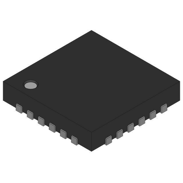


 工商网监
湘ICP备2023018690号
工商网监
湘ICP备2023018690号
