NB3M8T3910GEVB
NB3M8T3910G Evaluation
Board User's Manual
Introduction
The NB3M8T3910GEVB is a custom evaluation board
developed by ON Semiconductor for the NB3M8T3910G.
This evaluation board was designed to provide a flexible and
convenient platform to quickly evaluate, characterize and
verify the operation of the NB3M8T3910G.
This evaluation board manual contains:
• Information on the NB3M8T3910G Evaluation Board
• Assembly Instructions
• Test and Measurement Setup Procedures
• Bill of Materials
http://onsemi.com
EVAL BOARD USER’S MANUAL
This manual should be used in conjunction with the device
datasheet NB3M8T3910/D which contains full technical
details on the device specifications and operation.
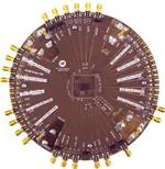
Top View
Bottom View
Figure 1. NB3M8T3910GEVB Top and Bottom View
READ FIRST − INTRODUCTION
The Single-Ended LVCMOS Output, REFOUT, is
controlled by the Synchronous OE_SE pin. For Clock
frequencies above 250 MHz, the REFOUT line should be
disabled.
Each dedicated output pair on the board is configured per
Table 1 below:
The NB3M8T3910G has two banks of 5 differential
outputs. Each output bank can be independently selected as
LVPECL, LVDS or HCSL outputs by the SMODEAx/Bx
select pins.
This evaluation board, NB3M8T3910GEVB, has been
configured to evaluate each output type.
Of the ten possible differential outputs, three are dedicated
as LVPECL, three are dedicated as LVDS and four are
dedicated as HCSL (labeled on board).
© Semiconductor Components Industries, LLC, 2014
September, 2014 − Rev. 0
1
Publication Order Number:
EVBUM2238/D
�NB3M8T3910GEVB
Table 1. OUTPUT DEDICATION OF THE NB3M8T3910GEVB
Output Pin Name
Output Type
(Dedicated)
SMODEA [1:0]
SMODEB [1:0]
QA0/QA0b
LVPECL
00
xx
Use 50-W Scope Head; there is no load on the board
QA1/QA1b
LVPECL
00
xx
Use 50-W Scope Head; there is no load on the board
QA2/QA2b
LVDS
01
xx
Measure with Single or Differential Hi-Z Probes; Outputs
have 100-W termination resistor across at SMA
connectors
QA3/QA3b
HCSL
10
xx
Use 50-W Scope Head; there is no 50-W to GND on the
board; or install 50-W SMA terminators and use a Hi-Z
probe
QA4/QA4b
HCSL
10
xx
Use 50-W Scope Head; there is no 50-W to GND on the
board; or install 50-W SMA terminators and use a Hi-Z
probe
QB0/QB0b
LVPECL
xx
00
Measure with Single or Differential Hi-Z Probes; these
LVPECL outputs have a Thevenin termination resistor
network.
QB1/QB1b
LVDS
xx
01
Measure with Single or Differential Hi-Z Probes; Outputs
have 100-W termination resistor across at SMA
connectors
QB2/QB2b
LVDS
xx
01
Measure with Single or Differential Hi-Z Probes; Outputs
have 100-W termination resistor across at SMA
connectors
QB3/QB3b
HCSL
xx
10
Measure with Single or Differential Hi-Z Probes; there is
50-W to GND on the board
QB4/QB4b
HCSL
xx
10
Use 50-W Scope Head; there is no 50-W to GND on the
board; or install 50-W SMA terminators and use a Hi-Z
probe
Output Measurement Method
NOTE: x = don’t care
LVDS OUTPUT CONFIGURATION
Two 0-W Resistors
100-W Resistor
Figure 2. LVDS Output Configuration
LVDS outputs. Two 0-Ω resistors connect the metal traces
and a 100-Ω resistor connects between the traces.
Use a single-ended or differential high-impedance probe
across the 100-Ω resistor.
LVDS outputs are typically terminated with 100-Ω across
the Q & Qb output pair.
On QA2/QA2b, QB1/QB1b, QB2/QB2b, there are
on-board 100-ohm output termination resistors across the
http://onsemi.com
2
�NB3M8T3910GEVB
HCSL OUTPUT CONFIGURATION
Rseries = 33-W for HCSL Outputs
CL = 2 pF Capacitor
to GND for HCSL
Outputs
Figure 3. HCSL Output Configuration
HCSL outputs are typically loaded and terminated with
a Rseries = 33-W and 50-W to ground. This can be easily
accomplished by connecting the HCSL outputs to the 50-W
internal impedance in the oscilloscope.
On QA3/QA3b, QA4/QA4b, QB3/QB3b, QB4/QB4b,
there are on-board Rseries = 33-W series termination resistors
installed for each HCSL output. Also, there is a CL = 2 pF
installed to GND.
For QA3/QA3b, QA4/QA4b, QB4/QB4b use 50-W to
GND of oscilloscope sampling head to satisfy the HCSL
output loading. QB3/QB3b has a 50-W output load, thus use
a Hi-Z probe for measurements.
LVPECL OUTPUT CONFIGURATION
RThevenin = 130-W to VCC (H) and
80-W to GND (L) for LVPECL Outputs
Figure 4. LVPECL Output Configuration
Figure 5. LVPECL Output Configuration,
Thevenin Termination Resistors
On QA0/QA0b or QA1/QA1b, there is no on-board
LVPECL output loading or termination.
Use the 50-W to GND of the oscilloscope sampling head
to satisfy the LVPECL output loading and termination. This
single supply scheme will simplify the LVPECL output
testing versus a split power supply. However, this method
will actually draw more output current with a single power
supply versus a dual/split power supply. Nevertheless, this
extra output current will be within the Maximum Ratings
limit.
On QB0/QB0b, there is an on-board Thevenin output
loading and termination resistor network; 130-W from
LVPECL output to VDDO and 80-W from output to GND.
This arrangement will satisfy the LVPECL DC output
loading and AC termination.
Use single-ended or differential high-impedance probes.
See AND8020/D, section 3, for more information.
http://onsemi.com
3
�NB3M8T3910GEVB
QUICK START LAB SET-UP USER’S GUIDE
“Split” or Dual Power Supply Connections
Dual Power Supply
1. Connect the VDD and VDDOx banana jacks with
power supply cables to +3.3 V, and DUTGND
and SMAGND to 0 V.
2. Select Crystal input and monitor 25 MHz on each
Qn output.
3. Connect a signal generator to the SMA connectors
for CLK0/CLK0b or CLK1/CLK1b inputs.
50-ohm termination resistors are installed for
a signal generator on the board. Set appropriate
input signal levels and frequency.
4. Observe the Qn outputs with a high-Z probe
oscilloscope.
+1.3 V
+2.0 V
+
Power-Up, Input and Output Connections
+
−
VCC
−
SMAGND DUTGND
+3.3 V
Figure 6. LVPECL – “Split” or Dual Power Supply
Configuration
Most ECL outputs are open emitter and need to be DC
loaded and AC terminated to VCC – 2.0 V via a 50 W
resistor. For standard ECL lab setup and test, a split (dual)
power supply is recommended enabling the 50-W internal
impedance in the oscilloscope, or other measuring
instrument, to be used as an ECL output load/termination.
By offsetting VCC = +2.0 V, SMAGND = VCC – 2.0 V =
0 V, SMAGND is the system ground, 0 V, and DUTGND is
–1.3 V or −0.5 V.
More information on ECL termination is provided in
AND8020/D.
Table 2. POWER SUPPLY CONNECTIONS
Device Pin
Power Supply Connector
Power Supply
VDD
+3.3 V
VDDOx
+3.3 V
SMAGND
0V
DUTGND
0V
Power Supply Connector
“Spilt” Power Supply
Single Power Supply Connections
VDD/VDDOx
VCC = +2.0 V
Single Power Supply
SMAGND
VTT = 0 V
DUTGND
DUTGND = −1.3 V for 3.3 V
p/s or −0.5 V for 2.5 V p/s
+3.3 V
+
LVCMOS OUTPUT CONFIGURATION
On REFOUT use a Hi−Z probe or the following set up to
use a 50 W to GND sampling head Oscilloscope.
0V
−
VDD/VDDOx
SMAGND/DUTGND
“Split” or Dual Power Supply Connections
+3.3 V
Dual Power Supply
Figure 8. Single Power Supply Configuration
+1.65 V
+
−
VCC
+
+1.65 V
−
SMAGND DUTGND
+3.3 V
Figure 7. LVCMOS – “Split” or Dual Power Supply
Configuration
http://onsemi.com
4
�NB3M8T3910GEVB
VDDOC
VDD
VDDOB
Signal Generator
Oscilloscope
OUT
Q
OUTb
Qb
Trigger In
Trigger Out
SMAGND
VDDOA
DUTGND
Figure 9. Typical Lab Test Set-Up
Board Layout
second layer is the 0.5 oz copper ground plane and is
dedicated for the SMA connector ground plane. FR4
dielectric material is placed between the second and third
layers and between third and fourth layers. The third layer
is also 0.5 oz copper plane. A portion of this layer is
designated for the device VDD and DUTGND power
planes. The fourth layer is the VDDOx layer.
The custom QFN−48 Evaluation Board provides a high
bandwidth, 50-W controlled impedance environment and is
implemented in four layers. The first layer or primary
“high-speed” trace layer is FR4 material, and is designed to
have equal electrical length on all signal traces from the
device under test (DUT) pins to the SMA connectors. The
Layer Stack
L1 (top) High Speed Signal (FR4)
L2 SMAGND − SMA Ground (FR4)
L3 VDD and DUTGND (FR4)
L4 (bottom) VDDOx and DUTGND (FR4)
Figure 10. QFN−48 Evaluation Board Layout, 4-Layer Stack
DUTGND (Device Under Test Ground) is the negative
power supply for the device. Banana jack is labeled
DUTGND.
Exposed Pad (EP). The exposed pad footprint on the board
is mechanically connected (soldered) to the exposed pad of
the QFN−48 package, and is electrically connected to
DUTGND power supply.
Table 2 and Figure 8 describes the board configuration for
the power supplies, Figure 3 shows typical input and output
connections.
VDD is the positive power supply.
VDDOA, VDDOB, VDDOC are the positive power
supplies for the outputs.
http://onsemi.com
5
�NB3M8T3910GEVB
SMAGND is the ground for the SMA connectors, is always
0 V and is not to be confused with the device ground,
DUTGND. SMAGND and DUTGND can be connected in
single-supply applications.
Power Supply Configuration
Install the power supply banana jacks on the bottom side;
install the appropriate bypass capacitors on top and bottom
sides.
The positive power supply banana jack connector for the
core and inputs is labeled VDD.
The positive power supply banana jack connector for the
outputs is labeled VDDOA/B/C.
The device negative power supply banana jack connector is
labeled DUTGND.
The SMA Ground plane/supply banana jack connector is
labeled SMAGND.
XTAL_IN Crystal
A 25 MHz crystal is installed. Set the SELx pins in
Table 3 of datasheet to select crystal. 27 pF load capacitors
are installed.
If a single-ended Clock input is needed to drive
XTAL_IN, then remove the crystal and load capacitor, and
install a 0-ohm resistor on RX1 and a 50-ohm resistor on
RT1 on bottom side. This 50-ohm to GND will terminate the
signal generator. Use the XTAL_IN SMA connector.
The power supply banana jacks and typical capacitor
by-pass connections of the evaluation board are shown in
Figure 11.
It is recommended to add power supply bypass capacitors
at the device pins to reduce unwanted noise.
10 mF capacitors are connected from VDD and VDDOx
and DUTGND, to SMAGND at the banana jacks.
A 0.1 mF capacitor is installed from each VDD and
VDDOx pin to SMAGND.
Evaluation Board Assembly Instructions
The NB3M8T3910GEVB evaluation board was designed
for characterizing devices in a 50-W laboratory environment
using high bandwidth equipment and accommodates
a custom QFN−48 socket. Table 3 contains the Bill of
Materials for this evaluation board.
Solder the Device on the Evaluation Board
The soldering of a QFN−48 package to the evaluation
board can be accomplished by hand soldering or solder
reflow techniques using solder paste and a hot air source.
Make sure pin 1 of the device is located properly and all the
pins are aligned to the footprint pads. Solder the device to the
evaluation board.
NOTE: Exposed Pad = DUTGND
VCC
VDDO
10 mF, 0.1 mF
Installing the SMA Connectors
Each high-speed input and output has an SMA connector
installed on the board. Install all the required SMA
connectors onto the board and solder the center signal
conductor pin to the board. Please note that the alignment of
the center signal connector pin of the SMA connector to the
metal trace on the board can influence lab results.
The launch and reflection of the signals are largely
influenced by imperfect alignment and soldering of the
SMA connector.
SMAGND
10 mF, 0.1 mF
DUTGND
Figure 11. Typical Power Supply By-Pass
Capacitor Arrangement
http://onsemi.com
6
�NB3M8T3910GEVB
LVPECL QA1/QA1b 50-W TO GND OF OSCILLOSCOPE
Figure 12. 50 MHz
Figure 13. 100 MHz
Figure 14. 250 MHz
Figure 15. 500 MHz
Figure 16. 1000 MHz
Figure 17. 1250 MHz
http://onsemi.com
7
�NB3M8T3910GEVB
LVPECL QA1/QA1b 50-W TO GND OF OSCILLOSCOPE
Figure 18. 1500 MHz
http://onsemi.com
8
�NB3M8T3910GEVB
LVPECL QB0/QB0b HI-Z PROBE OSCILLOSCOPE
Figure 19. 50 MHz
Figure 20. 100 MHz
Figure 21. 250 MHz
Figure 22. 500 MHz
Figure 23. 1000 MHz
Figure 24. 1250 MHz
http://onsemi.com
9
�NB3M8T3910GEVB
LVPECL QB0/QB0b HI-Z PROBE OSCILLOSCOPE
Figure 25. 1500 MHz
http://onsemi.com
10
�NB3M8T3910GEVB
LVDS QB1/QB1b SINGLE-ENDED HI-Z PROBE OSCILLOSCOPE
Figure 26. 50 MHz
Figure 27. 100 MHz
Figure 28. 250 MHz
Figure 29. 500 MHz
Figure 30. 1000 MHz
Figure 31. 1250 MHz
http://onsemi.com
11
�NB3M8T3910GEVB
LVDS QB1/QB1b SINGLE-ENDED HI-Z PROBE OSCILLOSCOPE
Figure 32. 1500 MHz
http://onsemi.com
12
�NB3M8T3910GEVB
LVDS QB1/QB1b DIFFERENTIAL HI-Z PROBE OSCILLOSCOPE
Figure 33. 50 MHz
Figure 34. 100 MHz
Figure 35. 250 MHz
Figure 36. 500 MHz
Figure 37. 1000 MHz
Figure 38. 1250 MHz
http://onsemi.com
13
�NB3M8T3910GEVB
LVDS QB1/QB1b DIFFERENTIAL HI-Z PROBE OSCILLOSCOPE
Figure 39. 1500 MHz
http://onsemi.com
14
�NB3M8T3910GEVB
HCSL QA3/QA3b 50-W TO GND OF OSCILLOSCOPE
Figure 40. 50 MHz
Figure 41. 100 MHz
Figure 42. 250 MHz
http://onsemi.com
15
�NB3M8T3910GEVB
HCSL QB3/QB3b HI−Z PROBE OSCILLOSCOPE
Figure 43. 50 MHz
Figure 44. 100 MHz
Figure 45. 250 MHz
http://onsemi.com
16
�NB3M8T3910GEVB
LVCMOS REFOUT
Figure 46. 50 MHz
Figure 47. 100 MHz
Figure 48. 200 MHz
http://onsemi.com
17
�NB3M8T3910GEVB
BILL OF MATERIALS
Table 3. NB3M8T3910GEVB BILL OF MATERIALS
Component
Qty.
Description
Manufacturer
Part Number
SMA Connector
32
Edge Mount
Johnson
142-0711-821
Web Site
Banana Jack
Connector
4
Red − Side Launch
Deltron
571-0500
Mouser #164-6219
Banana Jack
Connector
2
Black − Side Launch
Deltron
571-0100
Mouser #164-6218
Chip Resistor
R1, R2, R3, R4,
R6, R7, R30, R31,
R33-R36, R44
13 + 6
0-W 0402
Vishay
CRCW04020000Z0ED
Digi-Key
541-0.0JCT-ND
Chip Resistor
R9-R12, R25-R28
8
33-W 0402
Panasonic
ERJ-2RKF33R0X
Digi-Key
ERJ-2RKF33R0X
Chip Resistor
R20, R21, R40,
R41
4
50-W 1%, 0402
Vishay
FC0402E50R0FST1
Digi-Key
FC0402E50R0FST1-ND
Chip Resistor
3
100-W 0402
Vishay
FC0402E1000FST1
Digi-Key
FC0402E1000FST1-ND
Chip Resistor
R38
1
475-W 0402
Vishay
MCS04020C4750FE000
Digi-Key
2312 275 14751-ND
2
27 pF Crystal Load
Capacitor
5
10 mF ±10%, Case
“C” 25 V or 16 V
KEMET
T491C106K025AT
T491C106K016AS
Chip Capacitor
C6, C57, C58, C59,
C64, C72, C80,
C81, C91-C96
14
0.1 mF ±10%, 0603
0.1 mF ±10%, 0402
AVX
0603C104KAT2A
0402ZD104KAT2A
www.avx.com
Digi-Key 478-1129-1-ND
Chip Capacitor
6
2 pF
TDK
C1005C0G1H020C
Digi-Key 445-4863-1-ND
Header
J14, J19, J22, J23,
J39, J46, J47
7
3-Pin3 Header,
thru-hole 0.1
3M
Shunt
7
QPC02SXGN-RC
Digi-Key
S9337-ND or
A26229-ND
Crystal
1
25 MHz Crystal
Abracon
Crystal
Receptacles
2
Pin Receptacle,
Amp, .140 lg, Max
pin .021 Tin, Gold
Mill-Max
0462-0-15-01-11-02-04-0
Digi-Key
0462-015011102040-ND
Stand-off
4
Standoff, 4-40
1/4 × 5/8
Keystone
1808
Digi-Key 1808K-ND
Screw
4
Screw, 4-40 × 0.25,
PHP
Building Fasteners
PMS 440 0025 PH
Digi-Key H342-ND
Evaluation Board
1
NB3M8T3910GEVB
QFN-48 Evaluation
Board
ON Semiconductor
NB3M8T3910GEVB
Device Under Test
1
DUT
ON Semiconductor
NB3M8T3910G
Sullins
NOTE: Components are available through most distributors, i.e. www.newark.com, www.Digikey.com
http://onsemi.com
18
www.onsemi.com
�onsemi,
, and other names, marks, and brands are registered and/or common law trademarks of Semiconductor Components Industries, LLC dba “onsemi” or its affiliates
and/or subsidiaries in the United States and/or other countries. onsemi owns the rights to a number of patents, trademarks, copyrights, trade secrets, and other intellectual property. A
listing of onsemi’s product/patent coverage may be accessed at www.onsemi.com/site/pdf/Patent−Marking.pdf. onsemi is an Equal Opportunity/Affirmative Action Employer. This
literature is subject to all applicable copyright laws and is not for resale in any manner.
The evaluation board/kit (research and development board/kit) (hereinafter the “board”) is not a finished product and is not available for sale to consumers. The board is only intended
for research, development, demonstration and evaluation purposes and will only be used in laboratory/development areas by persons with an engineering/technical training and familiar
with the risks associated with handling electrical/mechanical components, systems and subsystems. This person assumes full responsibility/liability for proper and safe handling. Any
other use, resale or redistribution for any other purpose is strictly prohibited.
THE BOARD IS PROVIDED BY ONSEMI TO YOU “AS IS” AND WITHOUT ANY REPRESENTATIONS OR WARRANTIES WHATSOEVER. WITHOUT LIMITING THE FOREGOING,
ONSEMI (AND ITS LICENSORS/SUPPLIERS) HEREBY DISCLAIMS ANY AND ALL REPRESENTATIONS AND WARRANTIES IN RELATION TO THE BOARD, ANY
MODIFICATIONS, OR THIS AGREEMENT, WHETHER EXPRESS, IMPLIED, STATUTORY OR OTHERWISE, INCLUDING WITHOUT LIMITATION ANY AND ALL
REPRESENTATIONS AND WARRANTIES OF MERCHANTABILITY, FITNESS FOR A PARTICULAR PURPOSE, TITLE, NON−INFRINGEMENT, AND THOSE ARISING FROM A
COURSE OF DEALING, TRADE USAGE, TRADE CUSTOM OR TRADE PRACTICE.
onsemi reserves the right to make changes without further notice to any board.
You are responsible for determining whether the board will be suitable for your intended use or application or will achieve your intended results. Prior to using or distributing any systems
that have been evaluated, designed or tested using the board, you agree to test and validate your design to confirm the functionality for your application. Any technical, applications or
design information or advice, quality characterization, reliability data or other services provided by onsemi shall not constitute any representation or warranty by onsemi, and no additional
obligations or liabilities shall arise from onsemi having provided such information or services.
onsemi products including the boards are not designed, intended, or authorized for use in life support systems, or any FDA Class 3 medical devices or medical devices with a similar
or equivalent classification in a foreign jurisdiction, or any devices intended for implantation in the human body. You agree to indemnify, defend and hold harmless onsemi, its directors,
officers, employees, representatives, agents, subsidiaries, affiliates, distributors, and assigns, against any and all liabilities, losses, costs, damages, judgments, and expenses, arising
out of any claim, demand, investigation, lawsuit, regulatory action or cause of action arising out of or associated with any unauthorized use, even if such claim alleges that onsemi was
negligent regarding the design or manufacture of any products and/or the board.
This evaluation board/kit does not fall within the scope of the European Union directives regarding electromagnetic compatibility, restricted substances (RoHS), recycling (WEEE), FCC,
CE or UL, and may not meet the technical requirements of these or other related directives.
FCC WARNING – This evaluation board/kit is intended for use for engineering development, demonstration, or evaluation purposes only and is not considered by onsemi to be a finished
end product fit for general consumer use. It may generate, use, or radiate radio frequency energy and has not been tested for compliance with the limits of computing devices pursuant
to part 15 of FCC rules, which are designed to provide reasonable protection against radio frequency interference. Operation of this equipment may cause interference with radio
communications, in which case the user shall be responsible, at its expense, to take whatever measures may be required to correct this interference.
onsemi does not convey any license under its patent rights nor the rights of others.
LIMITATIONS OF LIABILITY: onsemi shall not be liable for any special, consequential, incidental, indirect or punitive damages, including, but not limited to the costs of requalification,
delay, loss of profits or goodwill, arising out of or in connection with the board, even if onsemi is advised of the possibility of such damages. In no event shall onsemi’s aggregate liability
from any obligation arising out of or in connection with the board, under any theory of liability, exceed the purchase price paid for the board, if any.
The board is provided to you subject to the license and other terms per onsemi’s standard terms and conditions of sale. For more information and documentation, please visit
www.onsemi.com.
PUBLICATION ORDERING INFORMATION
LITERATURE FULFILLMENT:
Email Requests to: orderlit@onsemi.com
onsemi Website: www.onsemi.com
◊
TECHNICAL SUPPORT
North American Technical Support:
Voice Mail: 1 800−282−9855 Toll Free USA/Canada
Phone: 011 421 33 790 2910
www.onsemi.com
1
Europe, Middle East and Africa Technical Support:
Phone: 00421 33 790 2910
For additional information, please contact your local Sales Representative
�