ON Semiconductor
Is Now
To learn more about onsemi™, please visit our website at
www.onsemi.com
onsemi and and other names, marks, and brands are registered and/or common law trademarks of Semiconductor Components Industries, LLC dba “onsemi” or its affiliates and/or
subsidiaries in the United States and/or other countries. onsemi owns the rights to a number of patents, trademarks, copyrights, trade secrets, and other intellectual property. A listing of onsemi
product/patent coverage may be accessed at www.onsemi.com/site/pdf/Patent-Marking.pdf. onsemi reserves the right to make changes at any time to any products or information herein, without
notice. The information herein is provided “as-is” and onsemi makes no warranty, representation or guarantee regarding the accuracy of the information, product features, availability, functionality,
or suitability of its products for any particular purpose, nor does onsemi assume any liability arising out of the application or use of any product or circuit, and specifically disclaims any and all
liability, including without limitation special, consequential or incidental damages. Buyer is responsible for its products and applications using onsemi products, including compliance with all laws,
regulations and safety requirements or standards, regardless of any support or applications information provided by onsemi. “Typical” parameters which may be provided in onsemi data sheets and/
or specifications can and do vary in different applications and actual performance may vary over time. All operating parameters, including “Typicals” must be validated for each customer application
by customer’s technical experts. onsemi does not convey any license under any of its intellectual property rights nor the rights of others. onsemi products are not designed, intended, or authorized
for use as a critical component in life support systems or any FDA Class 3 medical devices or medical devices with a same or similar classification in a foreign jurisdiction or any devices intended for
implantation in the human body. Should Buyer purchase or use onsemi products for any such unintended or unauthorized application, Buyer shall indemnify and hold onsemi and its officers, employees,
subsidiaries, affiliates, and distributors harmless against all claims, costs, damages, and expenses, and reasonable attorney fees arising out of, directly or indirectly, any claim of personal injury or death
associated with such unintended or unauthorized use, even if such claim alleges that onsemi was negligent regarding the design or manufacture of the part. onsemi is an Equal Opportunity/Affirmative
Action Employer. This literature is subject to all applicable copyright laws and is not for resale in any manner. Other names and brands may be claimed as the property of others.
�NB4L16M
2.5�V/3.3�V, 5 Gb/s Multi Level
Clock/Data Input to CML
Driver/Receiver/Buffer/
Translator with Internal
Termination
www.onsemi.com
Description
The NB4L16M is a differential driver/receiver/buffer/translator
which can accept LVPECL, LVDS, CML, HSTL, LVCMOS/LVTTL
and produce 400 mV CML output. The device is capable of receiving,
buffering, and translating a clock or data signal that is as small as
75 mV operating up to 3.5 GHz or 5.0 Gb/s, respectively. As such, it is
ideal for SONET, GigE, Fiber Channel and backplane applications
(see Table 6 and Figures 20, 21 22, and 23).
Differential inputs incorporate internal 50 W termination resistors
and accept LVPECL (Positive ECL), LVTTL/LVCMOS, CML, HSTL
or LVDS. The differential 16 mA CML output provides matching
internal 50 W termination, and 400 mV output swing when externally
receiver terminated, 50 W to VCC (see Figure 19). These features
provide transmission line termination on chip, at the receiver and
driver end, eliminating any use of additional external components.
The VBB, an internally generated voltage supply, is available to this
device only. For single-ended input configuration, the unused
complementary differential input is connected to VBB as a switching
reference voltage. The VBB reference output can be used also to
re-bias capacitor coupled differential or single-ended output signals.
For the capacitor coupled input signals, VBB should be connected to
the VTD pin and bypassed to ground with a 0.01 mF capacitor. When
not used VBB should be left open.
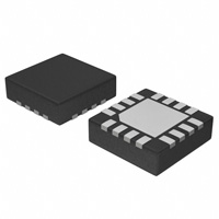
This device is housed in a 3x3 mm 16 pin QFN package.
Application notes, models, and support documentation are available at
www.onsemi.com.
Features
•
•
•
•
•
•
•
•
•
•
•
Maximum Input Clock Frequency up to 3.5 GHz
Maximum Input Data Rate up to 5.0 Gb/s
< 0.7 ps Maximum Clock RMS Jitter
< 10 ps Maximum Data Dependent Jitter at 2.5 Gb/s
220 ps Typical Propagation Delay
60 ps Typical Rise and Fall Times
CML Output with Operating Range:
♦ VCC = 2.375 V to 3.6 V with VEE = 0 V
CML Output Level (400 mV Peak-to-Peak Output),
Differential Output Only
50 W Internal Input and Output Termination Resistors
Functionally Compatible with Existing 2.5 V / 3.3 V LVEL, LVEP,
EP, and SG Devices
These Devices are Pb-Free, Halogen Free and are RoHS Compliant
© Semiconductor Components Industries, LLC, 2016
October, 2018 − Rev. 5
1
1
QFN−16
MN SUFFIX
CASE 485G−01
MARKING DIAGRAM*
16
1
NB4L
16M
ALYWG
G
A
L
Y
W
G
= Assembly Location
= Wafer Lot
= Year
= Work Week
= Pb-Free Package
(Note: Microdot may be in either location)
*For additional marking information, refer to
Application Note AND8002/D.
ORDERING INFORMATION
Package
Shipping†
NB4L16MMNG
QFN−16
(Pb-Free)
123 Units/Tube
NB4L16MMNR2G
QFN−16
(Pb-Free)
3000/Tape & Reel
Device
†For information on tape and reel specifications, including part orientation and tape sizes, please refer
to our Tape and Reel Packaging Specifications
Brochure, BRD8011/D.
Publication Order Number:
NB4L16M/D
�NB4L16M
VCC
VCC
16
VBB VEE VEE
15
14
Exposed Pad (EP)
13
VTD
50 W
R1
R2
D
Q
D
Q
50 W
R2
VTD
1
D
2
12 VCC
11 Q
NB4L16M
R1
D
3
10 Q
VTD
4
9
VCC
VTD
VEE
5
6
7
VCC
NC
VEE
8
VEE
Figure 2. Pin Configuration (Top View)
Figure 1. Functional Block Diagram
Table 1. PIN DESCRIPTION
Pin
Name
I/O
Description
1
VTD
−
2
D
LVPECL, CML, HSTL,
LVCMOS, LVDS, LVTTL Input
Inverted differential input. Internal 36.5 kW to VCC and 73 kW to VEE
(Note 1).
3
D
LVPECL, CML, HSTL,
LVCMOS, LVDS, LVTTL Input
Non-inverted differential input. Internal 73 kW to VCC and 36.5 kW to VEE
(Note 1).
4
VTD
−
Internal 50 W termination pin. See Table 4. (Note 1)
15
VBB
−
Internally generated reference voltage supply.
6
NC
10
Q
CML Output
Non-inverted differential output. Typically receiver terminated with 50 W
resistor to VCC.
11
Q
CML Output
Inverted differential output. Typically receiver terminated with 50 W resistor
to VCC.
7, 8, 13, 14
VEE
−
Negative supply voltage
5, 9, 12, 16
VCC
−
Positive supply voltage
−
EP
−
Exposed pad (EP). EP on the package bottom is thermally connected to the
die for improved heat transfer out of the package. The pad is not electrically
connected to the die, but is recommended to be soldered to VEE on the
PC Board.
Internal 50 W termination pin. See Table 4 (Note 1).
No Connect pin. The No Connect (NC) pin is electrically connected to the
die and MUST be left open.
1. In the differential configuration when the input termination pins (VTD, VTD) are connected to a common termination voltage and if no signal
is applied on D/D input then the device will be susceptible to self-oscillation.
www.onsemi.com
2
�NB4L16M
Table 2. ATTRIBUTES
Characteristics
Value
Input Default State Resistors
R1
R2
37.5 kW
73 kW
ESD Protection
Human Body Model
Machine Model
Charged Device Model
> 2 kV
> 200 V
> 1 kV
Moisture Sensitivity (Note 1)
Pb-Free Pkg
QFN−16
Level 1
Flammability Rating
Oxygen Index: 28 to 34
UL 94 V−0 @ 0.125 in
Transistor Count
157
Meets or exceeds JEDEC Spec EIA/JESD78 IC Latchup Test
1. For additional information, see Application Note AND8003/D.
Table 3. MAXIMUM RATINGS
Symbol
Rating
Unit
VCC
Positive Power Supply
VEE = 0 V
6
V
VEE
Negative Power Supply
VCC = 0 V
−6
V
Positive Input
Negative Input
VEE = 0 V
VCC = 0 V
6
−6
V
Differential Input Voltage
|D − D|
|VCC − VEE|
V
Input Current Through RT (50 W Resistor)
Static
Surge
45
80
mA
Output Current
Continuous
Surge
25
50
mA
VI
VINPP
IIN
IOUT
Parameter
Condition 1
Condition 2
VI = VCC
VI = VEE
IBB
VBB Sink/Source
± 0.5
mA
TA
Operating Temperature Range
−40 to +85
°C
Tstg
Storage Temperature Range
−65 to +150
°C
qJA
Thermal Resistance (Junction-to-Ambient) (Note 1)
0 lfpm
500 lfpm
QFN−16
42
35
°C/W
qJC
Thermal Resistance (Junction-to-Case)
1S2P (Note 1)
QFN−16
4
°C/W
Tsol
Wave Solder (Pb-Free)
265
°C
Stresses exceeding those listed in the Maximum Ratings table may damage the device. If any of these limits are exceeded, device functionality
should not be assumed, damage may occur and reliability may be affected.
1. JEDEC standard multilayer board − 1S2P (1 signal, 2 power) with 8 filled thermal vias under exposed pad.
www.onsemi.com
3
�NB4L16M
Table 4. DC CHARACTERISTICS, CLOCK INPUTS, CML OUTPUTS (VCC= 2.375 V to 3.8 V, VEE = 0 V, TA = −40°C to +85°C)
Symbol
Characteristic
Min
Typ
Max
Unit
30
45
55
mA
Output HIGH Voltage (Note 1)
VCC − 40
VCC − 10
VCC
mV
Output LOW Voltage (Note 1)
VCC − 500
VCC − 400
VCC − 300
mV
VCC − 150
mV
ICC
Power Supply Current (Inputs and Outputs Open)
VOH
VOL
DIFFERENTIAL INPUT DRIVEN SINGLE-ENDED (Figures 15 and 17)
VTH
Input Threshold Reference Voltage Range (Note 3)
1050
VIH
Single-ended Input HIGH Voltage
Vth + 150
VCC
mV
VIL
Single-ended Input LOW Voltage
VEE
Vth − 150
mV
VBB
Internally Generated Reference Voltage Supply (Loaded with −100 mA)
VCC − 1300
mV
VCC − 1500
VCC − 1400
DIFFERENTIAL INPUTS DRIVEN DIFFERENTIALLY (Figures 16 and 18)
VIHD
Differential Input HIGH Voltage
1200
VCC
mV
VILD
Differential Input LOW Voltage
VEE
VCC − 150
mV
VCMR
Input Common Mode Range (Differential Configuration)
950
VCC – 75
mV
VID
Differential Input Voltage (VIHD − VILD)
150
VCC – VEE
mV
IIH
Input HIGH Current (VTD/VTD Open)
D
D
0
0
100
50
150
100
IIL
Input LOW Current (VTD/VTD Open)
D
D
−100
−150
−50
−100
0
0
Internal Input Termination Resistor
40
50
60
W
RTOUT
Internal Output Termination Resistor
40
50
60
W
RTemp
Internal I/O Termination Resistor Temperature Coefficient
RTIN
16
mA
mA
mW/°C
Coef
NOTE: Device will meet the specifications after thermal equilibrium has been established when mounted in a test socket or printed circuit
board with maintained transverse airflow greater than 500 lfpm. Electrical parameters are guaranteed only over the declared
operating temperature range. Functional operation of the device exceeding these conditions is not implied. Device specification limit
values are applied individually under normal operating conditions and not valid simultaneously.
1. CML outputs require 50 W receiver termination resistors to VCC for proper operation. See Figure 14.
2. Input and output parameters vary 1:1 with VCC.
3. Vth is applied to the complementary input when operating in single-ended mode.
4. VCMR min varies 1:1 with VEE, VCMRmax varies 1:1 with VCC. The VCMR range is referenced to the most positive side of the differential
input signal.
www.onsemi.com
4
�NB4L16M
Table 5. AC CHARACTERISTICS (VCC = 2.375 V to 3.8 V, VEE = 0 V; (Note 1))
−40°C
Symbol
VOUTPP
Characteristic
Min
Typ
25°C
Max
Min
Typ
85°C
Max
Min
Typ
Max
Unit
Output Voltage Amplitude (@VINPPmin)
(Figures 3 and 4)
fin ≤ 3.5 Ghz
fin ≤ 4.5 GHz
280
150
400
300
280
150
400
300
280
150
400
300
fDATA
Maximum Operating Data Rate
3.5
5.0
3.5
5.0
3.5
5.0
tPLH,
tPHL
Propagation Delay to Output
Differential @ 0.5 Ghz (Figure 6)
175
215
265
175
220
265
175
225
265
ps
tSKEW
Duty Cycle Skew (Note 2)
Device-to-Device Skew (Note 6)
2.0
6.0
10
90
2.0
6.0
10
90
2.0
6.0
10
90
ps
tJITTER
RMS Random Clock Jitter (Note 4)
fin ≤ 4.5 GHz
Peak-to-Peak Data Dependent Jitter (Note 5)
fDATA = 2.5 Gb/s
fDATA = 3.5 Gb/s
fDATA = 5.0 Gb/s
0.2
0.7
0.2
0.7
0.2
0.7
1.5
2.0
9.0
10
12
25
1.5
2.0
9.0
10
12
25
1.5
2.0
9.0
10
12
25
VINPP
tr
tf
Input Voltage Swing/Sensitivity
(Differential Configuration) (Note 3)
mV
75
VCC
−VEE
Output Rise/Fall Times @ 0.5 Ghz (Figure 5)
(20% − 80%)
60
90
75
VCC
−VEE
60
90
75
Gb/s
VCC
−VEE
60
ps
mV
90
ps
NOTE: Device will meet the specifications after thermal equilibrium has been established when mounted in a test socket or printed circuit
board with maintained transverse airflow greater than 500 lfpm. Electrical parameters are guaranteed only over the declared
operating temperature range. Functional operation of the device exceeding these conditions is not implied. Device specification limit
values are applied individually under normal operating conditions and not valid simultaneously.
1. Measured by forcing VINPP(MIN) from a 50% duty cycle clock source. All loading with an external RL = 50 W to VCC. Input edge rates 40 ps
(20% − 80%). See Figure 12 and 14.
2. Duty cycle skew is measured between differential outputs using the deviations of the sum of Tpw− and Tpw+ @ 0.5 GHz.
3. VINPP(MAX) cannot exceed VCC − VEE. Input voltage swing is a single-ended measurement operating in differential mode. See Figure 11.
4. Additive RMS jitter with 50% duty cycle input clock signal.
5. Additive peak-to-peak data dependent jitter with NRZ input data signal, PRBS 223−1 and K28.7 pattern. See Figures 7, 8, 9, 10, 11 and 12.
6. Device-to-device skew is measured between outputs under identical transition @ 0.5 GHz.
www.onsemi.com
5
�NB4L16M
450
OUTPUT VOLTAGE AMPLITUDE (mV)
OUTPUT VOLTAGE AMPLITUDE (mV)
TYPICAL OPERATING CHARACTERISTICS
400
350
−40°C
300
+85°C
250
+25°C
200
150
100
50
0
0
2
2.5
3
3.5
4
4.5
5
5.5
450
400
350
−40°C
300
+85°C
250
200
150
+25°C
100
50
0
0
INPUT CLOCK FREQUENCY (GHz)
3
3.5
4
4.5
5
5.5
Figure 4. Output Voltage Amplitude (VOUTPP)
vs Input Clock Frequency (fin) and
Temperature at 2.5 V Power Supply
90
265
255
80
245
70
235
VCC = 3.3 V
TIME (ps)
TIME (ps)
2.5
INPUT CLOCK FREQUENCY (GHz)
Figure 3. Output Voltage Amplitude (VOUTPP)
vs. Input Clock Frequency (fin) and
Temperature at 3.3 V Power Supply
60
50
VCC = 2.5 V
VCC = 3.3 V
225
215
205
VCC = 2.5 V
195
40
30
−40
2
185
25
175
−40
85
25
85
TEMPERATURE (°C)
TEMPERATURE (°C)
Figure 5. Rise/Fall Time vs Temperature and
Power Supply
Figure 6. Propagation Delay vs Temperature
and Power Supply
www.onsemi.com
6
�VOLTAGE (50 mV/div)
Device DDJ = 1.5 ps
Device DDJ = 2 ps
TIME (60 ps/div)
Figure 7. Typical Output Waveform at 2.488 Gb/s
with PRBS 223−1 (VINPP = 75 mV; Input Signal
DDJ = 12 ps)
Figure 8. Typical Output Waveform at 3.2 Gb/s
with PRBS 2^23−1 (VINPP = 75 mV; Input Signal
DDJ = 12 ps)
VOLTAGE (64 mV/div)
TIME (80 ps/div)
Device DDJ = 1.5 ps
Device DDJ = 2 ps
TIME (72 ps/div)
TIME (60 ps/div)
Figure 9. Typical Output Waveform at 2.488 Gb/s
with PRBS 223−1 (VINPP = 400 mV; Input Signal
DDJ = 12 ps)
Figure 10. Typical Output Waveform at 3.2 Gb/s
with PRBS 223−1 (VINPP = 400 mV; Input Signal
DDJ = 12 ps)
VOLTAGE (64 mV/div)
VOLTAGE (64 mV/div)
VOLTAGE (64 mV/div)
VOLTAGE (50 mV/div)
NB4L16M
Device DDJ = 9 ps
Device DDJ = 14 ps
TIME (43 ps/div)
TIME (36 ps/div)
Figure 11. Typical Output Waveform at 5 Gb/s
with PRBS 223−1 (VINPP = 400 mV;
Input Signal DDJ = 13 ps)
Figure 12. Typical Output Waveform at 6.125 Gb/s
with PRBS 223−1 (VINPP = 400 mV;
Input Signal DDJ = 15 ps)
www.onsemi.com
7
�NB4L16M
D
VINPP = VIH(D) − VIL(D)
D
Q
VOUTPP = VOH(Q) − VOL(Q)
Q
tPHL
tPLH
Figure 13. AC Reference Measurement
VCC
50 W
50 W
Zo = 50 W
Q
D
Receiver
Device
Driver
Device
Q
D
Zo = 50 W
Figure 14. Typical Termination for Output Driver and Device Evaluation
D
D
Vth
D
D
Vth
Figure 15. Differential Input Driven
Single-Ended
VCC
Vthmax
Figure 16. Differential Inputs Driven
Differentially
VCC
VCMmax
VIHmax
VILmax
Vth
Vthmin
GND
VIH
Vth
VIL
VIHDmax
VILDmax
VIHDtyp
VCMR
VID = VIHD − VILD
VILDtyp
VIHmin
VCMmax
VILmin
GND
Figure 17. Vth Diagram
NOTE:
VIHDmin
VILDmin
Figure 18. VCMR Diagram
VEEĂV VINĂV VCC; VIH > VIL
www.onsemi.com
8
�NB4L16M
VCC
50 W
50 W
Q
Q
16 mA
VEE
Figure 19. CML Output Structure
Table 6. INTERFACING OPTIONS
INTERFACING OPTIONS
CONNECTIONS
CML
Connect VTD and VTD to VCC
LVDS
Connect VTD and VTD Together
AC-COUPLED
RSECL, PECL, NECL
LVTTL, LVCMOS
Bias VTD and VTD Inputs within Common Mode Range (VCMR)
Standard ECL Termination Techniques
An External Voltage (VTHR) should be applied to the unused complementary differential input. Nominal
VTHR is 1.5 V for LVTTL and VCC/2 for LVCMOS inputs. This voltage must be within the VTHR specification.
www.onsemi.com
9
�NB4L16M
APPLICATION INFORMATION
All NB4L16M inputs can accept LVPECL, CML, LVTTL, LVCMOS and LVDS signal levels. The limitations for differential
input signal (LVDS, PECL, or CML) are minimum input swing of 75 mV and the maximum input swing of 2500 mV. Within
these conditions, the input voltage can range from VCC to 1.2 V. Examples interfaces are illustrated below in a 50 W
environment (Z = 50ĂW).
VCC
50 W
VCC
50 W
Q
D
Z
VCC
VCC
VTD
VTD
Z
Q
50 W
50 W
D
VEE
VEE
Figure 20. CML to CML Interface
VCC
VCC
50 W
PECL
Driver
VBIAS
VBIAS
50 W
Recommended RT Values
VCC
RT
RT
5.0 V 290 W
3.3 V 150 W
2.5 V
80 W
VEE
D
Z
VTD
VTD
Z
50 W
50 W
D
RT
VEE
VEE
Figure 21. PECL to CML Receiver Interface
www.onsemi.com
10
�NB4L16M
VCC
LVDS
Driver
VCC
D
Z
VTD
50 W
VTD
50 W
Z
D
VEE
VEE
Figure 22. LVDS to CML Receiver Interface
VCC
VCC
D
Z
LVTTL/
LVCMOS
Driver
No Connect
No Connect
50 W
VTD
VTD
50 W
VREF
VEE
Recommended VREF Values
D
VREF
VCC
Figure 23. LVCMOS/LVTTL to CML Receiver Interface
www.onsemi.com
11
LVCMOS VCC * VEE
LVTTL
2
1.5 V
�NB4L16M
PACKAGE DIMENSIONS
QFN−16 3x3, 0.5P
CASE 485G−01
ISSUE F
D
ÇÇÇ
ÇÇÇ
ÇÇÇ
PIN 1
LOCATION
2X
A
B
L
DETAIL A
ALTERNATE TERMINAL
CONSTRUCTIONS
E
ÉÉ
ÉÉ
EXPOSED Cu
0.10 C
TOP VIEW
DETAIL B
0.05 C
NOTES:
1. DIMENSIONING AND TOLERANCING PER
ASME Y14.5M, 1994.
2. CONTROLLING DIMENSION: MILLIMETERS.
3. DIMENSION b APPLIES TO PLATED
TERMINAL AND IS MEASURED BETWEEN
0.25 AND 0.30 MM FROM TERMINAL.
4. COPLANARITY APPLIES TO THE EXPOSED
PAD AS WELL AS THE TERMINALS.
L1
0.10 C
2X
L
(A3)
A3
A1
DETAIL B
A
0.05 C
ÇÇ
ÉÉ
MOLD CMPD
ALTERNATE
CONSTRUCTIONS
NOTE 4
A1
SIDE VIEW
C
SEATING
PLANE
DIM
A
A1
A3
b
D
D2
E
E2
e
K
L
L1
MILLIMETERS
MIN
NOM MAX
0.80
0.90
1.00
0.00
0.03
0.05
0.20 REF
0.18
0.24
0.30
3.00 BSC
1.65
1.75
1.85
3.00 BSC
1.65
1.75
1.85
0.50 BSC
0.18 TYP
0.30
0.40
0.50
0.00
0.08
0.15
RECOMMENDED
SOLDERING FOOTPRINT*
0.10 C A B
16X
L
DETAIL A
D2
8
4
16X
16X
0.58
PACKAGE
OUTLINE
1
9
2X
E2
K
2X
1.84 3.30
1
16X
16
e
e/2
BOTTOM VIEW
16X
0.30
b
0.50
PITCH
0.10 C A B
0.05 C
NOTE 3
DIMENSIONS: MILLIMETERS
*For additional information on our Pb-Free strategy and soldering
details, please download the ON Semiconductor Soldering and
Mounting Techniques Reference Manual, SOLDERRM/D.
ON Semiconductor and
are trademarks of Semiconductor Components Industries, LLC dba ON Semiconductor or its subsidiaries in the United States and/or other countries.
ON Semiconductor owns the rights to a number of patents, trademarks, copyrights, trade secrets, and other intellectual property. A listing of ON Semiconductor’s product/patent
coverage may be accessed at www.onsemi.com/site/pdf/Patent−Marking.pdf. ON Semiconductor reserves the right to make changes without further notice to any products herein.
ON Semiconductor makes no warranty, representation or guarantee regarding the suitability of its products for any particular purpose, nor does ON Semiconductor assume any liability
arising out of the application or use of any product or circuit, and specifically disclaims any and all liability, including without limitation special, consequential or incidental damages.
Buyer is responsible for its products and applications using ON Semiconductor products, including compliance with all laws, regulations and safety requirements or standards,
regardless of any support or applications information provided by ON Semiconductor. “Typical” parameters which may be provided in ON Semiconductor data sheets and/or
specifications can and do vary in different applications and actual performance may vary over time. All operating parameters, including “Typicals” must be validated for each customer
application by customer’s technical experts. ON Semiconductor does not convey any license under its patent rights nor the rights of others. ON Semiconductor products are not
designed, intended, or authorized for use as a critical component in life support systems or any FDA Class 3 medical devices or medical devices with a same or similar classification
in a foreign jurisdiction or any devices intended for implantation in the human body. Should Buyer purchase or use ON Semiconductor products for any such unintended or unauthorized
application, Buyer shall indemnify and hold ON Semiconductor and its officers, employees, subsidiaries, affiliates, and distributors harmless against all claims, costs, damages, and
expenses, and reasonable attorney fees arising out of, directly or indirectly, any claim of personal injury or death associated with such unintended or unauthorized use, even if such
claim alleges that ON Semiconductor was negligent regarding the design or manufacture of the part. ON Semiconductor is an Equal Opportunity/Affirmative Action Employer. This
literature is subject to all applicable copyright laws and is not for resale in any manner.
PUBLICATION ORDERING INFORMATION
LITERATURE FULFILLMENT:
Literature Distribution Center for ON Semiconductor
19521 E. 32nd Pkwy, Aurora, Colorado 80011 USA
Phone: 303−675−2175 or 800−344−3860 Toll Free USA/Canada
Fax: 303−675−2176 or 800−344−3867 Toll Free USA/Canada
Email: orderlit@onsemi.com
◊
N. American Technical Support: 800−282−9855 Toll Free
USA/Canada
Europe, Middle East and Africa Technical Support:
Phone: 421 33 790 2910
www.onsemi.com
12
ON Semiconductor Website: www.onsemi.com
Order Literature: http://www.onsemi.com/orderlit
For additional information, please contact your local
Sales Representative
NB4L16M/D
�