NB4L339
2.5 V / 3.3 V Differential 2:1
Clock IN to Differential
LVPECL Clock Generator /
Divider / Fan-Out Buffer
http://onsemi.com
Multi−Level Inputs w/ Internal Termination
Description
The NB4L339 is a multi−function Clock generator featuring a 2:1
Clock multiplexer front end and simultaneously outputs a selection of
four different divide ratios from its four divider blocks; ÷1/÷2/÷4/÷8.
One divide block has a choice of ÷1 or ÷ 2.
The output of each divider block is fanned−out to two identical
differential LVPECL copies of the selected clock. All outputs provide
standard LVPECL voltage levels when externally terminated with a
50−ohm resistor to VCC − 2 V.
The differential Clock inputs incorporate internal 50−� termination
resistors and will accept LVPECL, CML or LVDS logic levels.
The common Output Enable pin (EN) is synchronous so that the
internal dividers will only be enabled/disabled when the internal clock
is in the LOW state. This avoids any chance of generating a runt clock
pulse on the internal clock when the device is enabled/disabled as can
happen with an asynchronous control. An internal runt pulse could
lead to losing synchronization between the internal divider stages. The
internal enable flip−flop is clocked on the falling edge of the input
clock. Therefore, all associated specification limits are referenced to
the negative edge of the clock input.
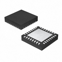
This device is housed in a 5x5 mm 32 pin QFN package.
MARKING
DIAGRAM
1
1
32
QFN32
MN SUFFIX
CASE 488AM
NB4L339
AWLYYWWG
G
A
= Assembly Location
WL
= Wafer Lot
YY
= Year
WW
= Work Week
G
= Pb−Free Package
(Note: Microdot may be in either location)
Features
•
•
•
•
•
•
•
•
•
•
•
•
•
•
•
•
Maximum Input/Output Clock Frequency > 700 MHz
Low Skew LVPECL Outputs, 15 ps typical
1 ns Typical Propagation Delay
150 ps Typical Rise and Fall Times
0.15 ps Typical RMS Phase Jitter
0.5 ps Typical RMS Random Clock Period Jitter
LVPECL, CML or LVDS Input Compatible
Operating Range: VCC = 2.375 V to 3.6 V with VEE = 0 V
LVPECL Output Level; 750 mV Peak−to−Peak, Typical
Internal 50−� Input Termination Provided
Synchronous Output Enable/Disable
Asynchronous Master Reset
Functionally Compatible with Existing 2.5 V / 3.3 V LVEL, LVEP,
EP, and SG Devices
−40°C to 85°C Ambient Operating Temperature
32−Pin QFN, 5 mm x 5 mm
This is a Pb−Free Device
Figure 1. Simplified Block Diagram
ORDERING INFORMATION
See detailed ordering and shipping information on page 11 of
this data sheet.
© Semiconductor Components Industries, LLC, 2012
September, 2012 − Rev. 3
1
Publication Order Number:
NB4L339/D
�NB4L339
DIVSEL
CLKSEL
CLKA
VTA
CLKA
A
÷1 / ÷2
R
A
QA0
QA0
QA1
QA1
foutA = 622.08 MHz
or 311.04 MHz
B
÷2
R
B
QB0
QB0
QB1
QB1
foutB = 311.04 MHz
C
÷4
R
C
QC0
QC0 foutC = 155.52 MHz
QC1
QC1
D
÷8
R
D
QD0
QD0
QD1
QD1
50−�
50−�
EXAMPLE: fin = 622.08 MHz
CLKB
VTB
CLKB
50−�
50−�
EN
EN
foutD = 77.76 MHz
MR
Figure 2. Detailed Logic Diagram
Table 1. Input Select Function Table
Table 2. Divider Select Function Table
CLKSEL*
CLK Input Selected
DIVSEL*
QA Divide
0
CLKA
0
Divide by 1
1
CLKB
1
Divide by 2
Table 3. Clock Enable/Disable Function Table
CLK Input
EN*
MR**
Function
Low to High Transition
0
H
Divide − Outputs Active
High to Low Transition
1
H
Hold Q − Outputs Inactive
X (Don’t Care)
X (Don’t Care)
L
Reset Q
VCC
MR
QA1
QA1
QA0
CLKA
2
26 25
24
Exposed Pad (EP)
23
VTA
3
22
QB1
CLKA
4
21
QB1
CLKB
5
20
QC0
VTB
6
19
QC0
CLKB
7
18
QC1
VEE
8
QC1
30 29 28 27
12 13 14
17
15 16
QD1
QD1
EN
VCC
11
QD0
10
QD0
9
CLKSEL
NB4L339
VCC
VEE
32 31
1
QA0
DIVSEL
** Pin will default HIGH when left OPEN.
VCC
* Pin will default LOW when left OPEN.
Figure 3. Pinout QFN−32 (Top View)
http://onsemi.com
2
QB0
QB0
�NB4L339
Table 4. Pin Description
Pin
Name
I/O
1, 8, EP
VEE
−
Description
2
CLKA
LVPECL, CML,
LVDS Input
3
VTA
−
4
CLKA
LVPECL, CML,
LVDS Input
Inverted differential input (A). (Note 1)
5
CLKB
LVPECL, CML,
LVDS Input
Non−inverted differential input (B). (Note 1)
6
VTB
−
7
CLKB
LVPECL, CML,
LVDS Input
9, 16,
25, 32
VCC
−
10
CLKSEL
LVCMOS/LVTTL
Asynchronous Clock input select pin. This pin defaults LOW when left open with 80 k�
resistor to VEE.
11
QD1
LVPECL Output
Inverted differential (D1) output. Typically terminated with 50 � resistor to VCC – 2 V
12
QD1
LVPECL Output
Non−inverted Differential (D1) Output. Typically terminated with 50 � resistor to VCC – 2 V.
13
QD0
LVPECL Output
Inverted differential (D0) output. Typically terminated with 50 � resistor to VCC – 2 V.
14
QD0
LVPECL Output
Non−inverted Differential (D0) Output. Typically terminated with 50 � resistor to VCC – 2 V.
15
EN
LVCMOS/LVTTL
Synchronous Output Enable/Disable pin. This pin defaults LOW when left open with 80 k�
resistor to VEE.
17
QC1
LVPECL Output
Inverted differential (C1) output. Typically terminated with 50 � resistor to VCC – 2 V.
18
QC1
LVPECL Output
Non−inverted Differential (C1) Output. Typically terminated with 50 � resistor to VCC – 2 V.
19
QC0
LVPECL Output
Inverted differential (C0) output. Typically terminated with 50 � resistor to VCC – 2 V.
20
QC0
LVPECL Output
Non−inverted Differential (C0) Output. Typically terminated with 50 � resistor to VCC – 2 V.
21
QB1
LVPECL Output
Inverted differential (B1) output. Typically terminated with 50 � resistor to VCC – 2 V.
22
QB1
LVPECL Output
Non−inverted Differential (B1) Output. Typically terminated with 50 � resistor to VCC – 2 V.
23
QB0
LVPECL Output
Inverted differential (B0) output. Typically terminated with 50 � resistor to VCC – 2 V.
24
QB0
LVPECL Output
Non−inverted Differential (B0) Output. Typically terminated with 50 � resistor to VCC – 2 V.
26
MR
LVCMOS/LVTTL
Master Reset Asynchronous. This pin defaults HIGH when left open with 80 k� resistor to
VCC.
27
QA1
LVPECL Output
Inverted differential (A1) output. Typically terminated with 50 � resistor to VCC – 2 V.
28
QA1
LVPECL Output
Non−inverted Differential (A1) Output. Typically terminated with 50 � resistor to VCC – 2 V.
29
QA0
LVPECL Output
Inverted differential (A0) output. Typically terminated with 50 � resistor to VCC – 2 V.
30
QA0
LVPECL Output
Non−inverted Differential (A0) Output. Typically terminated with 50 � resistor to VCC – 2 V.
31
DIVSEL
LVCMOS/LVTTL
Asynchronous Divide Select Pin selects A divide block outputs to divide by 1 or divide by 2.
Defaults LOW when left open, divide−by−1, with 80 k� resistor to VEE.
−
EP
−
Exposed Pad. The exposed pad (EP) on package bottom (see case drawing) is thermally
connected to the die for improved heat transfer out of package and must be attached to a
heat−sinking conduit. The pad is electrically connected to VEE and must be connected to
VEE on the PC board.
Negative Supply Voltage
Non−inverted differential input (A). (Note 1)
Internal 100−� center−tapped termination pin for CLKA and CLKA (Note 1).
Internal 100−� center−tapped termination pin for CLKB and CLKB. (Note 1)
Inverted differential input (B). (Note 1)
Positive Supply Voltage
1. In the differential configuration when the input termination pin (VTx / VTx) are connected to a common termination voltage or left open, and
if no signal is applied on CLKx / CLKx input then the device will be susceptible to self−oscillation.
http://onsemi.com
3
�NB4L339
Table 5. ATTRIBUTES
Characteristics
Value
Input Default State Resistors
80 k�
ESD Protection
Human Body Model
Machine Model
Moisture Sensitivity (Note 2)
QFN−32
Flammability Rating
Oxygen Index: 28 to 34
Transistor Count
> 2.0 kV
> 100 V
Level 1
UL 94 V−0 @ 0.125 in
366
Meets or exceeds JEDEC Spec EIA/JESD78 IC Latchup Test
2. For additional information, see Application Note AND8003/D.
Table 6. MAXIMUM RATINGS
Symbol
Parameter
VCC
Positive Power Supply
VIO
Input/Output Voltage
VINPP
IIN
Differential Input Voltage Swing
Condition 1
Condition 2
VEE = 0 V
VEE = 0 V
−0.5 = VIo ≤ VCC + 0.5
|CLK − CLK|
Rating
Units
4.0
V
4.0
V
2.8
V
Input Current Through RT (50 � Resistor)
Static
Surge
45
80
mA
Output Current
Continuous
Surge
50
100
mA
TA
Operating Temperature Range
QFN−32
−40 to +85
°C
Tstg
Storage Temperature Range
�JA
Thermal Resistance (Junction−to−Ambient) (Note 3)
0 LFPM
500 LFPM
QFN−32
QFN−32
�JC
Thermal Resistance (Junction−to−Case)
(Note 3)
QFN−32
Tsol
Wave Solder (Pb−Free)
IOUT
−65 to +150
°C
31
27
°C/W
12
°C/W
265
°C
Stresses exceeding Maximum Ratings may damage the device. Maximum Ratings are stress ratings only. Functional operation above the
Recommended Operating Conditions is not implied. Extended exposure to stresses above the Recommended Operating Conditions may affect
device reliability.
3. JEDEC standard multilayer board − 2S2P (2 signal, 2 power) with 8 filled thermal vias under exposed pad.
http://onsemi.com
4
�NB4L339
Table 7. DC CHARACTERISTICS, CLOCK Inputs, LVPECL Outputs
VCC = 2.375 V to 3.6 V, VEE = 0 V, TA = −40°C to +85°C (Note 5)
Symbol
IEE
Characteristic
Min
Typ
Max
Unit
58
70
90
mA
VCC − 1135
2155
1355
VCC − 1020
2280
1480
VCC − 760
2540
1740
mV
VCC = 3.3 V
VCC = 2.5 V
VCC − 1935
1355
555
VCC − 1770
1530
730
VCC − 1560
1740
940
mV
VCC = 3.3 V
VCC = 2.5 V
Power Supply Current (Inputs and Outputs Open)
LVPECL Outputs (Note 4)
VOH
VOL
Output HIGH Voltage
Output LOW Voltage
Differential Input Driven Single−Ended (see Figures 6 & 8)
Vth
Input Threshold Reference Voltage Range (Note 6)
1125
VCC − 75
mV
VIH
Single−ended Input HIGH Voltage
Vth + 75
VCC
mV
VIL
Single−ended Input LOW Voltage
VEE
Vth − 75
mV
VISE
Single−ended Input Voltage (VIH − VIL)
150
2800
mV
1200
VCC
mV
Differential Inputs Driven Differentially (see Figures 7 & 9)
VIHD
Differential Input HIGH Voltage
VILD
Differential Input LOW Voltage
VEE
VCC − 150
mV
VCMR
Input Common Mode Range (Differential Configuration) (Note 8)
1125
VCC − 75
mV
VID
Differential Input Voltage Swing (VIHD − VILD)
150
2800
mV
IIH
Input HIGH Current
CLKx / CLKx
(VTx Open)
10
40
�A
IIL
Input LOW Current
CLKx / CLKx
(VTx Open)
−10
10
�A
Single−Ended LVCMOS / LVTTL Control Inputs
VIH
Single−ended Input HIGH Voltage
2000
VCC
mV
VIL
Single−ended Input LOW Voltage
VEE
800
mV
IIH
Input HIGH Current
CLKSEL, DIVSEL, EN
MR
40
−10
115
10
�A
IIL
Input LOW Current
CLKSEL, DIVSEL, EN
MR
−10
−115
10
−40
�A
Termination Resistors
RTIN
Internal Input Termination Resistor (Measured across CLKx and CLKx)
80
100
120
�
RTIN
Internal Input Termination Resistor (Measured from CLKx to VTx)
40
50
60
�
NOTE: Device will meet the specifications after thermal equilibrium has been established when mounted in a test socket or printed circuit
board with maintained transverse airflow greater than 500 lfpm. Electrical parameters are guaranteed only over the declared
operating temperature range. Functional operation of the device exceeding these conditions is not implied. Device specification limit
values are applied individually under normal operating conditions and not valid simultaneously.
4. LVPECL outputs require 50 � receiver termination resistors to VCC − 2 V for proper operation.
5. Input and output parameters vary 1:1 with VCC.
6. Vth is applied to the complementary input when operating in single−ended mode.
7. VIHD, VILD, VID and VCMR parameters must be complied with simultaneously.
8. VCMR min varies 1:1 with VEE, VCMR max varies 1:1 with VCC. The VCMR range is referenced to the most positive side of the differential input
signal.
http://onsemi.com
5
�NB4L339
Table 8. AC CHARACTERISTICS VCC = 2.375 V to 3.6 V, VEE = 0 V (Note 9)
−40_C
Symbol
Min
Characteristic
Typ
finmax
Maximum Input CLOCK Frequency
700
VOUTPP
Output Voltage Amplitude (@ VINPPmin)
(See Figure 4)
fin ≤ 622 MHz
530
730
tPLH,
tPHL
Propagation Delay to
Output Differential ÷ 1
0.8
1.2
0.8
1.0
−
1.0
trr
Reset Recovery
DCO
Output CLOCK Duty Cycle
tSKEW
Within Device Skew (Note 11)
Device to Device Skew (Note 12)
ts
Setup Time @ 50 MHz
CLKx/CLKx to Qx/Qx
MR to Qx
CLKSEL to Qx
All Divides
Hold Time @ 50 MHz
CLKx to EN
CLKx to DIVSEL
tPW
Minimum Pulse Width
�N
Phase Noise
MR
Typ
85_C
Max
1.3
5.0
1.3
40
60
530
730
0.8
1.2
0.8
1.0
−
1.0
Typ
Max
1.3
5.0
1.3
60
30
90
530
730
0.8
1.2
0.8
1.0
−
1.0
mV
1.3
5.0
1.3
30
90
900
900
900
−100
−100
−100
800
800
800
0
0
0
5.0
5.0
5.0
ns
ns
40
60
190
Unit
MHz
4.0
40
60
190
Min
700
4.0
30
90
EN to CLKx
Min
700
4.0
DIVSEL to CLKx
th
25_C
Max
60
%
60
190
ps
ps
ps
ns
fin = 622.08 MHz
dBc
Outputs (A) Div by 1
tJIT1
tJIT2
10 kHz
−136
100 kHz
−136
1 MHz
−141
10 MHz
−141
20 MHz
−141
40 MHz
−141
Integrated Phase Jitter (Figure 4)
fin = 622.08 MHz, 12 kHz − 20 MHz Offset
All Divides
0.15
0.25
0.15
0.25
0.15
0.25
0.5
1.5
0.5
1.5
0.5
1.5
Random Clock Period Jitter (Note 13)
fin = 622.08 MHz
All Divides
VINPP
Input Voltage Swing/Sensitivity
(Differential Configuration) (Note 14)
tr, tf
Output Rise/Fall Times @ 622.08 MHz
input frequency (20% − 80%)
150
150
150
250
NOTE:
150
150
250
ps
RMS
ps
RMS
mV
150
250
ps
Device will meet the specifications after thermal equilibrium has been established when mounted in a test socket or printed circuit
board with maintained transverse airflow greater than 500 lfpm. Electrical parameters are guaranteed only over the declared
operating temperature range. Functional operation of the device exceeding these conditions is not implied. Device specification
limit values are applied individually under normal operating conditions and not valid simultaneously.
9. Measured by forcing VINPP (Min) from a 50% duty cycle clock source. All loading with an external RL = 50 � to VCC − 2 V Input edge rates
100 ps (20% − 80%).
10. Duty cycle skew is measured between differential outputs using the deviations of the sum of Tpw− and Tpw+ @ 50 MHz.
11. Skew is measured between outputs under identical transitions and conditions. Duty cycle skew is defined only for differential operation when
the delays are measured from the cross−point of the inputs to the cross−point of the outputs.
12. Device to device skew is measured between outputs under identical transition @ 50 MHz.
13. Additive RMS jitter with 50% duty cycle clock signal; all inputs and outputs active.
14. VINPP (Max) cannot exceed VCC − VEE. Input voltage swing is a single−ended measurement operating in differential mode.
http://onsemi.com
6
�NB4L339
VOUTPP, OUTPUT VOLTAGE AMPLITUDE (mV)
(TYPICAL)
Figure 4. NB4L339 vs. Agilent 8665A 622.08 MHz at 3.3 V, Room Ambient
800
700
600
500
400
300
200
100
0
0
0.1
0.2
0.3
0.4
0.5
0.6
0.7
0.8
0.9
1.0
1.1
1.2
fout, CLOCK OUTPUT FREQUENCY (GHz)
Figure 5. Output Voltage Amplitude (VOUTPP) vs. Input Clock Frequency (fin) at
Ambient Temperature (Typical)
Application Information
The NB4L339 is a high−speed, Clock multiplexer, divider
and low skew fan−out buffer featuring a 2:1 Clock
multiplexer front end and outputs a selection of four
different divide ratios; ÷1/2/4/8. One divide block has a
choice of ÷1 or ÷ 2. The outputs of all four divider blocks are
fanned−out to two pair of identical differential LVPECL
copies of the selected clock. All outputs provide standard
LVPECL voltage levels when externally terminated with a
50−ohm resistor to VTT = VCC − 2 V.
The differential Clock input buffers incorporate internal
50−� termination resistors in a 100−� center−tapped
configuration and are accessible via a VTx pin. This feature
provides transmission line termination on−chip, at the
receiver end, eliminating external components. Inputs
CLKA/B and CLKA/B must be signal driven or auto
oscillation may result.
The NB4L339 Clock inputs can be driven by a variety of
differential signal level technologies including LVDS,
LVPECL, or CML.
The internal dividers are synchronous to each other.
Therefore, the common output edges are precisely aligned.
The Output Enable pin (EN) is synchronous so that the
internal divider flip−flops will only be enabled/disabled
when the internal clock is in the LOW state. This avoids any
chance of generating a runt pulse on the internal clock when
the device is enabled/disabled, as can happen with an
asynchronous control. The internal enable flip−flop is
clocked on the falling edge of the input clock. Therefore, all
associated specification limits are referenced to the negative
edge of the clock input.
The Master Reset (MR) is asynchronous. When MR is
forced LOW, all Q outputs go to logic LOW.
http://onsemi.com
7
�NB4L339
MR
CLK
Q (÷1)
Q (÷2)
Q (÷4)
Q (÷8)
Figure 6. Timing Diagram
CLK
tRR
MR
tRR
Q (÷n)
NOTE: On the rising edge of MR, Q goes HIGH after the first rising edge of CLK, following a high−to−low clock transition.
Figure 7. Master Reset Timing Diagram
Internal Clock
Disabled
Internal Clock
Enabled
CLK
Q (÷n)
EN
Figure 8. Output Enable Timing Diagrams
The EN signal will “freeze” the internal divider flip−flops
on the first falling edge of CLK after its assertion. The
internal divider flip−flops will maintain their state during the
freeze. When EN is deasserted (LOW), and after the next
falling edge of CLK, then the internal divider flip−flops will
“unfreeze” and continue to their next state count with proper
phase relationships.
http://onsemi.com
8
�NB4L339
CLK
Vth
CLKn
50 �
VTn
Vth
50 �
CLK
Figure 10. Differential Input Driven Single−Ended
CLKn
Figure 9. Input Structure
CLK
VCC
VIHmax
Vthmax
Vth
CLK
VILmax
Figure 12. Differential Inputs Driven Differentially
VIH
Vth
VIL
CLK
VIHmin
Vthmin
VILmin
VEE
VCC
Figure 11. Vth Diagram
VIHDmax
VILDmax
VCMmax
CLK
VCMR
VIHDtyp
VILDtyp
CLK
CLK
CLK
VIHDmin
VCMmax
VID = |VIHD(CLK) − VILD(CLK)|
VILDmin
VIHD
VILD
VID = VIHD − VILD
VEE
Figure 13. Differential Inputs Driven Differentially
Figure 14. VCMR Diagram
CLK
VINPP = VIH(CLK) − VIL(CLK)
CLK
Q
VOUTPP = VOH(Q) − VOL(Q)
Q
tPHL
NOTE: VEE ≤ VIN ≤ VCC; VIH > VIL
tPLH
Figure 15. AC Reference Measurement
http://onsemi.com
9
�NB4L339
VCC
VCC
NB4L339
CLKx
Zo = 50 �
LVPECL
Driver
VCC
VT = VCC − 2.0 V
50 �
50 �
LVDS
Driver
VT = OPEN
50 �
Zo = 50 �
CLKx
CLKx
GND
CLKx
CLKx
GND
GND
Figure 16. LVPECL Interface
VCC
NB4L339
CLKx
Zo = 50 �
50 �
Zo = 50 �
VCC
GND
Figure 17. LVDS Interface
VCC
Zo = 50 �
NB4L339
CLKx
50 �
CML
Driver
VT = VCC
50 �
Zo = 50 �
GND
CLKx
GND
Figure 18. Standard 50 W Load CML Interface
VCC
VCC
Zo = 50 �
VCC
NB4L339
CLKx
VCC
Zo = 50 �
50 �
Differential
Driver
GND
50 �
Single−Ended
Driver
VT = VREFAC*
50 �
Zo = 50 �
NB4L339
CLKx
CLKx
VT = VREFAC*
50 �
CLKx (open)
GND
GND
Figure 19. Capacitor−Coupled Differential
Interface (VT Connected to External VREFAC)
GND
Figure 20. Capacitor−Coupled Single−Ended
Interface (VT Connected to External VREFAC)
*VREFAC bypassed to ground with a 0.01 �F capacitor.
http://onsemi.com
10
�NB4L339
ZO = 50 �
Q
Driver
Device
D
ZO = 50 �
Q
D
50 �
Receiver
Device
50 �
VTT
VTT = VCC − 2.0 V
Figure 21. Typical Termination for Output Driver and Device Evaluation
(See Application Note AND8020/D − Termination of ECL Logic Devices)
ORDERING INFORMATION
Package
Shipping†
NB4L339MNG
QFN32
(Pb−free)
74 Units / Tray
NB4L339MNR4G
QFN32
(Pb−free)
1000 / Tape & Reel
Device
*For additional information on our Pb−Free strategy and soldering details, please download the ON Semiconductor Soldering and Mounting
Techniques Reference Manual, SOLDERRM/D.
http://onsemi.com
11
�NB4L339
PACKAGE DIMENSIONS
QFN32 5x5, 0.5 P
CASE 488AM
ISSUE O
PIN ONE
LOCATION
2X
ÉÉ
ÉÉ
0.15 C
2X
A
B
D
NOTES:
1. DIMENSIONS AND TOLERANCING PER
ASME Y14.5M, 1994.
2. CONTROLLING DIMENSION: MILLIMETERS.
3. DIMENSION b APPLIES TO PLATED
TERMINAL AND IS MEASURED BETWEEN
0.25 AND 0.30 MM TERMINAL
4. COPLANARITY APPLIES TO THE EXPOSED
PAD AS WELL AS THE TERMINALS.
E
DIM
A
A1
A3
b
D
D2
E
E2
e
K
L
TOP VIEW
0.15 C
(A3)
0.10 C
A
32 X
0.08 C
C
L
32 X
9
D2
SEATING
PLANE
A1
SIDE VIEW
SOLDERING FOOTPRINT*
5.30
EXPOSED PAD
16
MILLIMETERS
MIN
NOM MAX
0.800 0.900 1.000
0.000 0.025 0.050
0.200 REF
0.180 0.250 0.300
5.00 BSC
2.950 3.100 3.250
5.00 BSC
2.950 3.100 3.250
0.500 BSC
0.200
−−−
−−−
0.300 0.400 0.500
K
32 X
17
3.20
8
32 X
0.63
E2
1
24
32
3.20
25
32 X b
0.10 C A B
5.30
e
0.05 C
32 X
0.28
BOTTOM VIEW
28 X
0.50 PITCH
*For additional information on our Pb−Free strategy and soldering
details, please download the ON Semiconductor Soldering and
Mounting Techniques Reference Manual, SOLDERRM/D.
ON Semiconductor and
are registered trademarks of Semiconductor Components Industries, LLC (SCILLC). SCILLC owns the rights to a number of patents, trademarks,
copyrights, trade secrets, and other intellectual property. A listing of SCILLC’s product/patent coverage may be accessed at www.onsemi.com/site/pdf/Patent−Marking.pdf. SCILLC
reserves the right to make changes without further notice to any products herein. SCILLC makes no warranty, representation or guarantee regarding the suitability of its products for any
particular purpose, nor does SCILLC assume any liability arising out of the application or use of any product or circuit, and specifically disclaims any and all liability, including without
limitation special, consequential or incidental damages. “Typical” parameters which may be provided in SCILLC data sheets and/or specifications can and do vary in different applications
and actual performance may vary over time. All operating parameters, including “Typicals” must be validated for each customer application by customer’s technical experts. SCILLC
does not convey any license under its patent rights nor the rights of others. SCILLC products are not designed, intended, or authorized for use as components in systems intended for
surgical implant into the body, or other applications intended to support or sustain life, or for any other application in which the failure of the SCILLC product could create a situation where
personal injury or death may occur. Should Buyer purchase or use SCILLC products for any such unintended or unauthorized application, Buyer shall indemnify and hold SCILLC and
its officers, employees, subsidiaries, affiliates, and distributors harmless against all claims, costs, damages, and expenses, and reasonable attorney fees arising out of, directly or indirectly,
any claim of personal injury or death associated with such unintended or unauthorized use, even if such claim alleges that SCILLC was negligent regarding the design or manufacture
of the part. SCILLC is an Equal Opportunity/Affirmative Action Employer. This literature is subject to all applicable copyright laws and is not for resale in any manner.
PUBLICATION ORDERING INFORMATION
LITERATURE FULFILLMENT:
Literature Distribution Center for ON Semiconductor
P.O. Box 5163, Denver, Colorado 80217 USA
Phone: 303−675−2175 or 800−344−3860 Toll Free USA/Canada
Fax: 303−675−2176 or 800−344−3867 Toll Free USA/Canada
Email: orderlit@onsemi.com
N. American Technical Support: 800−282−9855 Toll Free
USA/Canada
Europe, Middle East and Africa Technical Support:
Phone: 421 33 790 2910
Japan Customer Focus Center
Phone: 81−3−5817−1050
http://onsemi.com
12
ON Semiconductor Website: www.onsemi.com
Order Literature: http://www.onsemi.com/orderlit
For additional information, please contact your local
Sales Representative
NB4L339/D
�