NB4L858M 2.5V/3.3V, 3 GHz Dual Differential Clock/Data 2x2 Crosspoint Switch with CML Output and Internal Termination
Description
http://onsemi.com MARKING DIAGRAM*
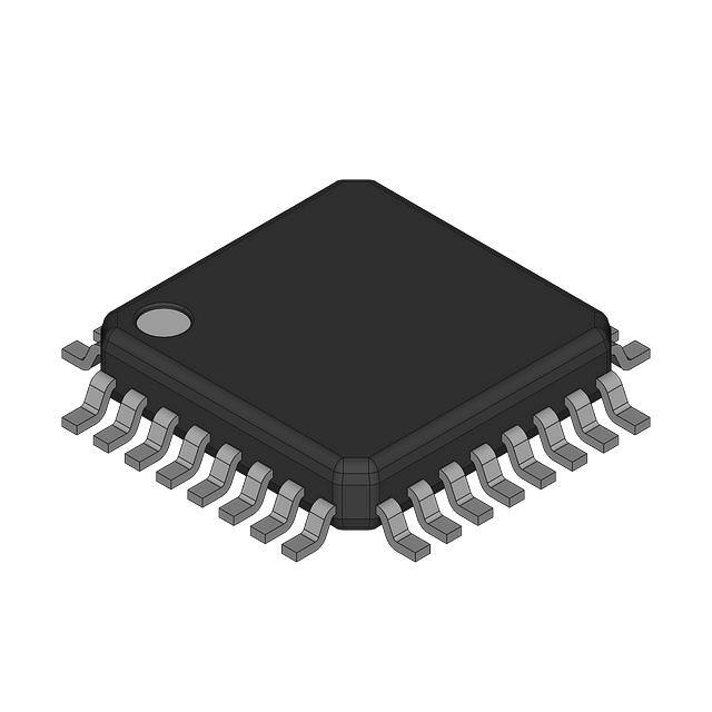
The NB4L858M is a high−bandwidth low voltage fully differential dual 2 x 2 crosspoint switch with CML outputs that is suitable for applications such as SDH/SONET DWDM and high speed switching applications. Design technique minimizes jitter accumulation, crosstalk, and signal skew which make this device ideal for loop−through and protection channel switching application. Each 2 x 2 crosspoint switch can fan out and/or multiplex up to 3 Gb/s data and 3 GHz clock signals. Differential inputs incorporate a pair of internal 50 W termination resistors in a center−tapped configuration (VTDx Pins) and can accept LVPECL (Positive ECL) or CML input signal without any external component. This feature provides transmission line termination on−chip, at the receiver end, eliminating external components. Differential 16 mA CML output provides matching internal 50 W terminations, and 400 mV output swings when externally terminated, 50 W to VCC. The SELECT inputs are single−ended and can be driven with either LVCMOS or LVTTL input levels. The device is housed in a low profile 7 x 7 mm 32−pin LQFP package.
Features
LQFP−32 FA SUFFIX CASE 873A
NB4L 858M AWLYYWW 32
A WL, L YY, Y WW, W G
1 = Assembly Location = Wafer Lot = Year = Work Week = Pb−Free Package
*For additional marking information, refer to Application Note AND8002/D.
SELA0 0 DA0 VTDA0 DA0 1 SELA1 0 DA1 VTDA1 DA1 1 SELB0 0 DB0 VTDB0 DB0 50W 50W B0 1 SELB1 0 DB1 VTDB1 DB1 1 50W 50W QB1 QB1 QB0 QB0 50W 50W QA1 QA1 50W 50W A0 QA0 QA0
• • • • • • • • • •
Maximum Input Clock Frequency 3 GHz Maximum Input Data Frequency 3 Gb/s 350 ps Typical Propagation Delay 80 ps Typical Rise and Fall Times 12 ps Channel to Channel Skew 0.5 ps RMS Jitter 5 ps Deterministic Jitter @ 2.5 Gb/s Operating Range: VCC = 2.3V to 3.6 V with GND = 0 V CML Output Level (400 mV Peak−to−Peak Output), Differential Output These are Pb−Free Devices
A1
B1
Figure 1. Functional Block Diagram ORDERING INFORMATION
See detailed ordering and shipping information in the package dimensions section on page 8 of this data sheet.
© Semiconductor Components Industries, LLC, 2005
1
December, 2005 − Rev. 9
Publication Order Number: NB4L858M/D
�NB4L858M
GND VCC QA0 QA0 VCC QA1 QA1 VCC
24 DA0 VTDA0 DA0 SELA1 DA1 VTDA1 DA1 SELA0 25 26 27 28 29 30 31 32 1
23
22
21
20
19
18
17 16 15 14 13 VCC QB1 QB1 VCC QB0 QB0 VCC GND
LQFP−32
12 11 10 9
2
3
4
5
6
7
8
DB1 VTDB1 DB1 SELB0 DB0 VTDB0 DB0 SELB1
Figure 1. Pin Configuration (Top View)
Table 1. TRUTH TABLE
SELA0/SELB0 L L H H SELA1/SELB1 L H L H QA0/QB0 DA0/DB0 DA0/DB0 DA1/DB1 DA1/DB1 QA1/QB1 DA0/DB0 DA1/DB1 DA0/DB0 DA1/DB1 Function 1:2 Fanout or Redundant Distribution Quad Repeater or Crosspoint Switch Quad Repeater or Crosspoint Switch 1:2 Fanout or Redundant Distribution
http://onsemi.com
2
�NB4L858M
Table 2. PIN DESCRIPTION
Pin 1 2 3 4 5 6 7 8 9,24 10, 13, 16, 17, 20, 23 11 12 14 15 18 19 21 22 25 26 27 28 29 30 31 32 Name DB1 VTDB1 DB1 SELB0 DB0 VTDB0 DB0 SELB1 GND VCC QB0 QB0 QB1 QB1 QA1 QA1 QA0 QA0 DA0 VTDA0 DA0 SELA1 DA1 VTDA1 DA1 SELA0 I/O LVPECL, CML Input − LVPECL, CML Input LVTTL / LVCMOS LVPECL, CML Input − LVPECL, CML Input LVTTL / LVCMOS − − CML Output CML Output CML Output CML Output CML Output CML Output CML Output CML Output LVPECL, CML Input − LVPECL, CML Input LVTTL LVPECL, CML Input − LVPECL, CML Input LVTTL Channel B1 positive signal input. Internal 100 W center−tapped termination pin for channel B1. Channel B1 negative signal input. Channel B0 Output Select. See Table 1. Channel B0 positive signal input. Internal 100 W center−tapped termination pin for channel B0. Channel B0 negative signal input. Channel B1 output select. See Table 1. Supply ground. All GND pins must be externally connected to power supply to guarantee proper operation. Positive Supply. All VCC pins must be externally connected to power supply to guarantee proper operation. Channel B0 negative signal output. Typically terminated with 50 W resistor to VCC. Channel B0 positive signal output. Typically terminated with 50 W resistor to VCC Channel B1 negative signal output. Typically terminated with 50 W resistor to VCC. Channel B1 positive signal output. Typically terminated with 50 W resistor to VCC. Channel A1 negative signal output. Typically terminated with 50 W resistor to VCC. Channel A1 positive signal output. Typically terminated with 50 W resistor to VCC. Channel A0 negative signal output. Typically terminated with 50 W resistor to VCC. Channel A0 positive signal output. Typically terminated with 50 W resistor to VCC. Channel A0 positive signal input. Internal 100 W center−tapped termination pin for channel A0. Channel A0 negative signal input. Channel A1 output select. See Table 1. Channel A1 positive signal input. Internal 100 W center−tapped termination pin for channel A1. Channel A1 negative signal input. Channel A0 output select. See Table 1. Description
http://onsemi.com
3
�NB4L858M
Table 3. Table 3. ATTRIBUTES
Characteristics ESD Protection Moisture Sensitivity (Note 1) Flammability Rating Transistor Count Meets or exceeds JEDEC Spec EIA/JESD78 IC Latchup Test 1. For additional information, see Application Note AND8003/D. Human Body Model Machine Model 32−LQFP Oxygen Index: 28 to 34 Value > 2000 V >110 V Level 2 UL 94 V−0 @ 0.125 in 380
Table 4. MAXIMUM RATINGS
Symbol VCC VI VINPP IIN IOUT TA Tstg qJA qJC Tsol Parameter Positive Power Supply Positive Input Differential Input Voltage |D − D| Static Surge Continuous Surge LQFP−32 Condition 1 GND = 0 V GND = 0 V GND v VI v VCC Condition 2 Rating 3.8 3.8 3.8 45 80 25 80 −40 to +85 −65 to +150 0 LFPM 500 LFPM 2S2P (Note 2)
很抱歉,暂时无法提供与“NB4L858MFAG”相匹配的价格&库存,您可以联系我们找货
免费人工找货