NB4N840M 3.3V 3.2Gb/s Dual Differential Clock/Data 2 x 2 Crosspoint Switch with CML Output and Internal Termination
Description
http://onsemi.com MARKING DIAGRAM
1
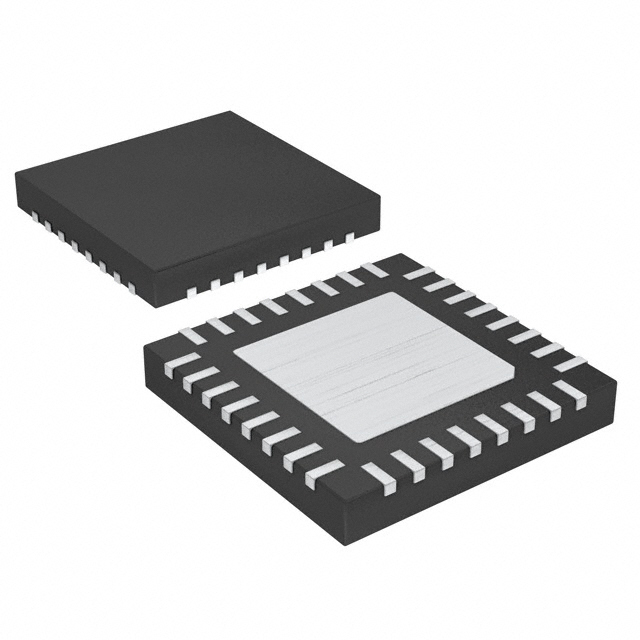
The NB4N840M is a high−bandwidth fully differential dual 2 x 2 crosspoint switch with CML inputs/outputs that is suitable for applications such as SDH/SONET, DWDM, Gigabit Ethernet and high speed switching. Fully differential design techniques are used to minimize jitter accumulation, crosstalk, and signal skew, which make this device ideal for loop−through and protection channel switching applications. Internally terminated differential CML inputs accept AC−coupled LVPECL (Positive ECL) or direct coupled CML signals. By providing internal 50 W input and output termination resistor, the need for external components is eliminated and interface reflections are minimized. Differential 16 mA CML outputs provide matching internal 50 W terminations, and 400 mV output swings when externally terminated, 50 W to VCC. Single−ended LVCMOS/LVTTL SEL inputs control the routing of the signals through the crosspoint switch which makes this device configurable as 1:2 fan−out, repeater or 2 x 2 crosspoint switch. The device is housed in a low profile 5 x 5 mm 32−pin QFN package.
Features
1
32
QFN32 MN SUFFIX CASE 488AM A WL YY WW G
DA0 DA0 CML
NB4N 840M ALYWG
= Assembly Location = Wafer Lot = Year = Work Week = Pb−Free Package
0 CML 1 QA0 ENA0 SELA0 0 QA1 CML QA1 ENA1 SELA1 QA0
DA1 DA1
CML
1
DB0 DB0
CML
0 1
QB0 CML QB0 ENB0 SELB0
• • • • • • • • • • • • •
Plug−in compatible to the MAX3840 and SY55859L Maximum Input Clock Frequency 2.7 GHz Maximum Input Data Frequency 3.2 Gb/s 225 ps Typical Propagation Delay 80 ps Typical Rise and Fall Times 7 ps Channel to Channel Skew 430 mW Power Consumption < 0.5 ps RMS Jitter 7 ps Peak−to−Peak Data Dependent Jitter Power Saving Feature with Disabled Outputs Operating Range: VCC = 3.0 V to 3.6 V with VEE = 0 V CML Output Level (400 mV Peak−to−Peak Output), Differential Output These are Pb−Free Devices
0 DB1 DB1 CML 1 CML
QB1 QB1 ENB1 SELB1
Figure 1. Functional Block Diagram ORDERING INFORMATION
See detailed ordering and shipping information on page 8 of this data sheet.
© Semiconductor Components Industries, LLC, 2006
1
August, 2006 − Rev. 2
Publication Order Number: NB4N840M/D
�NB4N840M
Table 1. TRUTH TABLE
SELA0/SELB0 L L H H X SELA1/SELB1 L H L H X ENA0/ENA1 H H H H L ENB0/ENB1 H H H H L QA0/QB0 DA0/DB0 DA0/DB0 DA1/DB1 DA1/DB1 Disable/Power Down QA1/QB1 DA0/DB0 DA1/DB1 DA0/DB0 DA1/DB1 Disable/Power Down Function 1:2 Fanout Quad Repeater Crosspoint Switch 1:2 Fanout No output (@ VCC)
SELA0
32 ENB1 DB1 DB1 ENB0 SELB0 DB0 DB0 SELB1 1 2 3 4
31
30
29
28
27
26
25 24 23 22 21 GND VCC QA0 QA0 VCC QA1 QA1 VCC
NB4N840M 5 6 7 8 9 GND 10 VCC 11 QB0 12 QB0 13 VCC 14 QB1 15 QB1 16 VCC 20 19 18 17
Figure 2. Pin Configuration (Top View)
http://onsemi.com
2
SELA1
ENA1
ENA0
DA1
DA1
DA0
DA0
�NB4N840M
Table 2. PIN DESCRIPTION
Pin 1 2 3 4 5 6 7 8 9,24 10, 13, 16, 17, 20, 23 11 12 14 15 18 19 21 22 25 26 27 28 29 30 31 32 − Name ENB1 DB1 DB1 ENB0 SELB0 DB0 DB0 SELB1 GND VCC QB0 QB0 QB1 QB1 QA1 QA1 QA0 QA0 SELA1 DA0 DA0 SELA0 ENA0 DA1 DA1 ENA1 EP I/O LVTTL CML Input CML Input LVTTL LVTTL CML Input CML Input LVTTL − − CML Output CML Output CML Output CML Output CML Output CML Output CML Output CML Output LVTTL CML Input CML Input LVTTL LVTTL CML Input CML Input LVTTL GND Description Channel B1 Output Enable. LVTTL low input powers down B1 output stage. Channel B1 Positive Signal Input Channel B1 Negative Signal Input Channel B0 Output Enable. LVTTL low input powers down B0 output stage. Channel B0 Output Select. See Table 1. Channel B0 Positive Signal Input Channel B0 Negative Signal Input Channel B1 Output Select. See Table 1. Supply Ground. All GND pins must be externally connected to power supply to guarantee proper operation. Positive Supply. All VCC pins must be externally connected to power supply to guarantee proper operation. Channel B0 Negative Output. Channel B0 Positive Output. Channel B1 Negative Output. Channel B1 Positive Output. Channel A1 Negative Output. Channel A1 Positive Output. Channel A0 Negative Output. Channel A0 Positive Output. Channel A1 Output Select, LVTTL Input. See Table 1. Channel A0 Positive Signal Input. Channel A0 Negative Signal Input. Channel A0 Output Select, LVTTL Input. See Table 1. Channel A0 Output Enable. LVTTL low input powers down A0 output stage. Channel A1 Positive Signal Input. Channel A1 Negative Signal Input. Channel A1 Output Enable. LVTTL low input powers down A1 output stage. Exposed Pad. The thermally exposed pad (EP) on package bottom (see case drawing) must be attached to a heat−sinking conduit. The exposed pad must be soldered to the circuit board GND for proper electrical and thermal operation.
http://onsemi.com
3
�NB4N840M
Table 3. ATTRIBUTES
Characteristics ESD Protection Moisture Sensitivity (Note 1) Flammability Rating Transistor Count Meets or exceeds JEDEC Spec EIA/JESD78 IC Latchup Test 1. For additional information, refer to Application Note AND8003/D. Human Body Model Machine Model QFN−32 Oxygen Index: 28 to 34 Value > 2000 V > 110 V Level 1 UL 94 V−0 @ 0.125 in 380
Table 4. MAXIMUM RATINGS
Symbol VCC VI VINPP IIN IOUT TA Tstg qJA qJC Tsol Parameter Positive Power Supply Positive Input Differential Input Voltage |D − D| Static Surge Continuous Surge QFN−32 Condition 1 GND = 0 V GND = 0 V GND = VI = VCC Condition 2 Rating 3.8 3.8 3.8 45 80 25 80 −40 to +85 −65 to +150 0 lfpm 500 lfpm 2S2P (Note 3)
很抱歉,暂时无法提供与“NB4N840MMNG”相匹配的价格&库存,您可以联系我们找货
免费人工找货