NB7V52M
D Flip Flop, 1.8 V / 2.5 V
Differential, with Reset and
CML Outputs
Multi−Level Inputs w/ Internal Termination
http://onsemi.com
MARKING
DIAGRAM*
Description
The NB7V52M is a 10 GHz differential D flip−flop with a
differential asynchronous Reset. The differential D/D, CLK/CLK and
R/R inputs incorporate dual internal 50 W termination resistors and
will accept LVPECL, CML, LVDS logic levels.
When Clock transitions from logic Low to High, Data will be
transferred to the differential CML outputs. The differential Clock
inputs allow the NB7V52M to also be used as a negative edge
triggered device.
The 16 mA differential CML outputs provide matching internal
50 W termination and produce 400 mV output swings when externally
receiver terminated with a 50 W resistor to VCC.
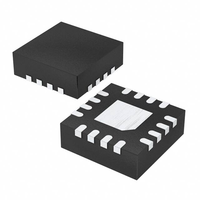
The NB7V52M is offered in a low profile 3 mm x 3 mm 16−pin
QFN package. The NB7V52M is a member of the GigaComm™
family of high performance clock products. Application notes,
models, and support documentation are available at
www.onsemi.com.
Features
•
•
•
•
•
•
•
•
•
•
•
Maximum Input Clock Frequency > 10 GHz
Maximum Input Data Rate > 10 Gb/s
Random Clock Jitter < 0.8 ps RMS, Max
200 ps Typical Propagation Delay
35 ps Typical Rise and Fall Times
Differential CML Outputs, 400 mV Peak−to−Peak, Typical
Operating Range: VCC = 1.71 V to 2.625 V with VEE = 0 V
Internal 50 W Input Termination Resistors
QFN−16 Package, 3mm x 3mm
−40°C to +85°C Ambient Operating Temperature
These are Pb−Free Devices
16
1
NB7V
52M
ALYWG
G
1
QFN−16
MN SUFFIX
CASE 485G
A
L
Y
W
G
= Assembly Location
= Wafer Lot
= Year
= Work Week
= Pb−Free Package
(Note: Microdot may be in either location)
*For additional marking information, refer to
Application Note AND8002/D.
VTD
D
D
VTD
D Flip−Flop
Q
VTCLK
Q
CLK
CLK
RESET
VTCLK
VTR
R R
VTR
Figure 1. Logic Diagram
ORDERING INFORMATION
See detailed ordering and shipping information in the package
dimensions section on page 9 of this data sheet.
© Semiconductor Components Industries, LLC, 2014
July, 2014 − Rev. 4
1
Publication Order Number:
NB7V52M/D
�NB7V52M
VTR
16
VTD
D
R
R
VTR
15
14
13
1
Exposed Pad (EP)
12
2
Table 1. INPUT/OUTPUT SELECT TRUTH TABLE
VCC
11
Q
NB7V52M
D
3
10
Q
VTD
4
9
VEE
5
VTCLK
6
7
R
D
CLK
Q
H
x
x
L
L
L
Z
L
L
H
Z
H
Z = LOW to HIGH Transition
x = Don’t care
8
CLK CLK VTCLK
Figure 2. Pin Configuration (Top View)
Table 1. Pin Description
Pin
Name
I/O
1
VTD
−
Description
2
D
LVPECL, CML,
LVDS Input
Noninverted Differential Data Input. (Note 1)
3
D
LVPECL, CML,
LVDS Input
Inverted Differential Data Input. (Note 1)
4
VTD
−
Internal 50 W Termination Pin for D
5
VTCLK
−
Internal 50 W Termination Pin for CLK
6
CLK
LVPECL, CML,
LVDS Input
Noninverted Differential Clock Input. (Note 1)
7
CLK
LVPECL, CML,
LVDS Input
Inverted Differential Clock Input. (Note 1)
8
VTCLK
−
Internal 50 W Termination Pin for CLK
9
VEE
−
Negative Supply Voltage. (Note 2)
10
Q
CML Output
Inverted Differential Output
11
Q
CML Output
Noninverted Differential Output
12
VCC
−
Positive Supply Voltage. (Note 2)
13
VTR
−
Internal 50 W Termination Pin for R
14
R
LVPECL, CML,
LVDS Input
Noninverted Asynchronous Differential Reset Input. (Note 1)
15
R
LVPECL, CML,
LVDS Input
Inverted Asynchronous Differential Reset Input. (Note 1)
16
VTR
−
Internal 50 W Termination Pin for R
−
EP
−
The Exposed Pad (EP) on the QFN−16 package bottom is thermally connected to the die for
improved heat transfer out of package. The exposed pad must be attached to a heat−sinking
conduit. The pad is electrically connected to the die, and must be electrically and thermally connected to VEE on the PC board.
Internal 50 W Termination Pin for D
1. In the differential configuration when the input termination pins (VTx, VTx) are connected to a common termination voltage or left open, and
if no signal is applied on CLK/CLK input, then the device will be susceptible to self−oscillation.
2. All VCC and VEE pins must be externally connected to a power supply for proper operation.
http://onsemi.com
2
�NB7V52M
Table 2. ATTRIBUTES
Characteristics
Value
ESD Protection
Human Body Model
Machine Model
Moisture Sensitivity
16−QFN
Flammability Rating
Oxygen Index: 28 to 34
> 2 kV
> 200 V
Level 1
UL 94 V−0 @ 0.125 in
Transistor Count
173
Meets or exceeds JEDEC Spec EIA/JESD78 IC Latchup Test
For additional information, see Application Note AND8003/D.
Table 3. MAXIMUM RATINGS
Symbol
Parameter
Condition 1
Condition 2
Rating
Unit
3.0
V
−0.5 to VCC +0.5
V
1.89
V
34
40
mA
$40
mA
−40 to +85
°C
VCC
Positive Power Supply
VEE = 0 V
VIO
Positive Input/Output Voltage
VEE = 0 V
VINPP
Differential Input Voltage |CLK − CLK|, |D − D|,
|R − R|
IOUT
Output Current Through RTOUT (50 W Resistor)
IIN
Input Current Through RTIN (50 W Resistor)
TA
Operating Temperature Range
Tstg
Storage Temperature Range
−65 to +150
°C
qJA
Thermal Resistance (Junction−to−Ambient)
(Note 3)
QFN−16
QFN−16
42
35
°C/W
°C/W
qJC
Thermal Resistance (Junction−to−Case) (Note 3)
QFN−16
4
°C/W
Tsol
Wave Solder
265
°C
−0.5 v VIO v VCC + 0.5
Continuous
Surge
0 lfpm
500 lfpm
Pb−Free
Stresses exceeding Maximum Ratings may damage the device. Maximum Ratings are stress ratings only. Functional operation above the
Recommended Operating Conditions is not implied. Extended exposure to stresses above the Recommended Operating Conditions may affect
device reliability.
3. JEDEC standard multilayer board − 2S2P (2 signal, 2 power) with 8 filled thermal vias under exposed pad.
http://onsemi.com
3
�NB7V52M
Table 4. DC CHARACTERISTICS, Multi−Level Inputs VCC = 1.71 V to 2.625 V, VEE = 0 V, TA = −40°C to +85°C (Note 4)
Symbol
Characteristic
Min
Typ
Max
Unit
90
70
110
90
mA
VCC – 30
2470
1770
VCC – 10
2490
1790
VCC
2500
1800
mV
VCC = 2.5 V
VCC – 650
1850
VCC – 500
2000
VCC – 400
2100
mV
VCC = 1.8 V
VCC – 600
1200
VCC – 450
1350
VCC – 350
1450
POWER SUPPLY CURRENT
ICC
Power Supply Current (Inputs and Outputs Open)
VCC = 2.5 V
VCC = 1.8 V
CML OUTPUTS
VOH
Output HIGH Voltage (Note 5)
VCC = 2.5 V
VCC = 1.8 V
VOL
Output LOW Voltage (Note 5)
DIFFERENTIAL CLOCK INPUTS DRIVEN SINGLE−ENDED (Note 6) (Figures 5 and 7)
Vth
Input Threshold Reference Voltage Range (Note 7)
1000
VCC − 100
mV
VIH
Single−Ended Input HIGH Voltage
Vth + 100
VCC
mV
VIL
Single−Ended Input LOW Voltage
VEE
Vth − 100
mV
VISE
Single−Ended Input Voltage (VIH − VIL)
200
1200
mV
DIFFERENTIAL D/D, CLK/CLK, R/R INPUTS DRIVEN DIFFERENTIALLY (Figures 6 and 8) (Note 8)
VIHD
Differential Input HIGH Voltage
1100
VCC
mV
VILD
Differential Input LOW Voltage
VEE
VCC − 100
mV
VID
Differential Input Voltage (VIHD − VILD)
100
1200
mV
VCMR
Input Common Mode Range (Differential Configuration, Note 9)
(Figure 10)
1050
VCC − 50
mV
IIH
Input HIGH Current (VTx/VTx Open)
−250
250
mA
IIL
Input LOW Current (VTx/VTx Open)
−250
250
mA
TERMINATION RESISTORS
RTIN
Internal Input Termination Resistor
45
50
55
W
RTOUT
Internal Output Termination Resistor
45
50
55
W
NOTE: Device will meet the specifications after thermal equilibrium has been established when mounted in a test socket or printed circuit
board with maintained transverse airflow greater than 500 lfpm. Electrical parameters are guaranteed only over the declared
operating temperature range. Functional operation of the device exceeding these conditions is not implied. Device specification limit
values are applied individually under normal operating conditions and not valid simultaneously.
4. Input and output parameters vary 1:1 with VCC.
5. CML outputs loaded with 50 W to VCC for proper operation.
6. Vth, VIH, VIL,, and VISE parameters must be complied with simultaneously.
7. Vth is applied to the complementary input when operating in single−ended mode.
8. VIHD, VILD, VID and VCMR parameters must be complied with simultaneously.
9. VCMR min varies 1:1 with VEE, VCMR max varies 1:1 with VCC. The VCMR range is referenced to the most positive side of the differential input
signal.
http://onsemi.com
4
�NB7V52M
Table 5. AC CHARACTERISTICS VCC = 1.71 V to 2.625 V; VEE = 0 V; TA = −40°C to 85°C (Note 10)
Symbol
Min
Typ
fMAX
Maximum Input Clock Frequency
Characteristic
10
12
GHz
fDATA MAX
Maximum Input Data Rate (PRBS23)
10
12
Gbps
VOUTPP
Output Voltage Amplitude (@ VINPPmin)
(See Figures 3 and 10, Note 11)
300
250
400
400
mV
tPLH,
tPHL
Propagation Delay to Differential Outputs, @ 1 GHz,
Measured at Differential Cross−point
tS
Setup Time (D to CLK)
tH
Hold Time (D to CLK)
tRR
Reset Recovery
tPW
Minimum Pulse Width
tJITTER
RJ – Output Random Jitter (Note 12)
VINPP
Input Voltage Swing (Differential Configuration) (Note 13)
tr,, tf
Output Rise/Fall Times @ 1 GHz (20% − 80%),
fin ≤ 7 GHz
fin ≤ 10 GHz
CLK/CLK to Q/Q
R/R to Q/Q
200
300
40
R/R
Max
350
600
ps
15
ps
50
20
ps
275
200
ps
1
fin v 10 GHz
ns
0.2
100
Q, Q
Unit
20
35
0.8
ps RMS
1200
mV
50
ps
NOTE: Device will meet the specifications after thermal equilibrium has been established when mounted in a test socket or printed circuit
board with maintained transverse airflow greater than 500 lfpm. Electrical parameters are guaranteed only over the declared
operating temperature range. Functional operation of the device exceeding these conditions is not implied. Device specification limit
values are applied individually under normal operating conditions and not valid simultaneously.
10. Measured using a 400 mV VINPP source, 50% duty cycle clock source. All output loading with external 50 W to VCC. Input edge rates
w40 ps (20% − 80%).
11. Output voltage swing is a single−ended measurement operating in differential mode.
12. Additive RMS jitter with 50% duty cycle clock signal.
13. Input voltage swing is a single−ended measurement operating in differential mode.
OUTPUT VOLTAGE AMPLITUDE
(mV)
500
VCC
450
VTD
Q/Q Output
50 W
400
RTIN
RC
RC
D
350
I
300
D
250
50 W
200
0
1
2
3
4
5
6
7
8
9
10
11 12
RTIN
VTD
fin, Clock Input Frequency (GHz)
Figure 3. Clock Output Voltage Amplitude
(VOUTPP) vs. Input Frequency (fin) at Ambient
Temperature (Typ)
Figure 4. Simplified Input Structure
http://onsemi.com
5
�NB7V52M
VIH
CLK
Vth
CLK/D/R
VIL
CLK
CLK/D/R
Vth
Figure 5. Differential Input Driven
Single−Ended
VCC
Vthmax
Figure 6. Differential Inputs
Driven Differentially
VIHmax
VILmax
Vth
CLK
VIH
Vth
VIL
CLK
CLK
VILD
VILmin
VEE
Figure 7. Vth Diagram
VCC
Figure 8. Differential Inputs Driven Differentially
VIHDmax
VCMRmax
CLK
VILDmax
CLK
VCMR
CLK
VEE
VIHD
VIHmin
Vthmin
VCMRmin
VID = |VIHD(CLK) − VILD(CLK)|
CLK
VIHDtyp
VID = VIHD − VILD
VINPP = VIH(CLK) − VIL(CLK)
Q
VILDtyp
Q
VIHDmin
VOUTPP = VOH(Q) − VOL(Q)
tPHL
VILDmin
tPLH
Figure 9. VCMR Diagram
Figure 10. AC Reference Measurement
http://onsemi.com
6
�NB7V52M
NB7V52M
VCC
50 W
RTOUT
Receiver
VCC
50 W
RTOUT
50 W
Q
50 W
Q
16 mA
VEE
Figure 11. Typical CML Output Structure and Termination
VCC
50 W
Z = 50 W
DUT
Driver
Device
50 W
Q
D
Receiver
Device
Z = 50 W
Q
D
Figure 12. Typical Termination for CML Output Driver and Device Evaluation
http://onsemi.com
7
�NB7V52M
VCC
VCC
ZO = 50 W
D
VCC
VCC
ZO = 50 W
NB7V52M
50 W
VTD
LVPECL
Driver
ZO = 50 W
VTD
LVDS
Driver
Vth
VTD
ZO = 50 W
50 W
D
VTD
NB7V52M
50 W
50 W
D
Vth = VCC − 2 V
GND/VEE
D
GND
VEE
VEE
Figure 13. LVPECL Interface
Figure 14. LVDS Interface
VCC
VCC
ZO = 50 W
CML
Driver
D
NB7V52M
50 W
VTD
VCC
ZO = 50 W
VT = VT = VCC
VTD
50 W
D
GND
VEE
Figure 15. Standard 50 W Load CML Interface
VCC
VCC
ZO = 50 W
Differential
Driver
Vth
ZO = 50 W
D
VTD
VTD
ZO = 50 W
NB7V52M
50 W
Single−Ended
Driver
50 W
D
Vth
D
VTD
VTD
NB7V52M
50 W
50 W
D
Vth = External VREFAC
GND/VEE
VCC
VCC
Vth = External VREFAC
GND/VEE
VEE
VEE
Figure 17. Capacitor−Coupled Single−Ended Interface
(VT/VT Connected to External VREFAC; VREFAC Bypassed
to Ground with 0.1 mF Capacitor)
Figure 16. Capacitor−Coupled Differential Interface
(VT/VT Connected to External VREFAC; VREFAC
Bypassed to Ground with 0.1 mF Capacitor)
http://onsemi.com
8
�NB7V52M
ORDERING INFORMATION
Package
Shipping†
NB7V52MMNG
QFN−16
(Pb−free)
123 Units / Rail
NB7V52MMNHTBG
QFN−16
(Pb−free)
100 / Tape & Reel
NB7V52MMNTXG
QFN−16
(Pb−free)
3000 / Tape & Reel
Device
†For information on tape and reel specifications, including part orientation and tape sizes, please refer to our Tape and Reel Packaging
Specifications Brochure, BRD8011/D.
GigaComm is a trademark of Semiconductor Components Industries, LLC (SCILLC).
http://onsemi.com
9
�MECHANICAL CASE OUTLINE
PACKAGE DIMENSIONS
QFN16 3x3, 0.5P
CASE 485G
ISSUE G
1
SCALE 2:1
DATE 08 OCT 2021
GENERIC
MARKING DIAGRAM*
XXXXX
XXXXX
ALYWG
G
XXXXX
A
L
Y
W
G
= Specific Device Code
= Assembly Location
= Wafer Lot
= Year
= Work Week
= Pb−Free Package
(Note: Microdot may be in either location)
*This information is generic. Please refer to
device data sheet for actual part marking.
Pb−Free indicator, “G” or microdot “G”, may
or may not be present. Some products may
not follow the Generic Marking.
DOCUMENT NUMBER:
DESCRIPTION:
98AON04795D
QFN16 3X3, 0.5P
Electronic versions are uncontrolled except when accessed directly from the Document Repository.
Printed versions are uncontrolled except when stamped “CONTROLLED COPY” in red.
PAGE 1 OF 1
onsemi and
are trademarks of Semiconductor Components Industries, LLC dba onsemi or its subsidiaries in the United States and/or other countries. onsemi reserves
the right to make changes without further notice to any products herein. onsemi makes no warranty, representation or guarantee regarding the suitability of its products for any particular
purpose, nor does onsemi assume any liability arising out of the application or use of any product or circuit, and specifically disclaims any and all liability, including without limitation
special, consequential or incidental damages. onsemi does not convey any license under its patent rights nor the rights of others.
© Semiconductor Components Industries, LLC, 2019
www.onsemi.com
�onsemi,
, and other names, marks, and brands are registered and/or common law trademarks of Semiconductor Components Industries, LLC dba “onsemi” or its affiliates
and/or subsidiaries in the United States and/or other countries. onsemi owns the rights to a number of patents, trademarks, copyrights, trade secrets, and other intellectual property.
A listing of onsemi’s product/patent coverage may be accessed at www.onsemi.com/site/pdf/Patent−Marking.pdf. onsemi reserves the right to make changes at any time to any
products or information herein, without notice. The information herein is provided “as−is” and onsemi makes no warranty, representation or guarantee regarding the accuracy of the
information, product features, availability, functionality, or suitability of its products for any particular purpose, nor does onsemi assume any liability arising out of the application or use
of any product or circuit, and specifically disclaims any and all liability, including without limitation special, consequential or incidental damages. Buyer is responsible for its products
and applications using onsemi products, including compliance with all laws, regulations and safety requirements or standards, regardless of any support or applications information
provided by onsemi. “Typical” parameters which may be provided in onsemi data sheets and/or specifications can and do vary in different applications and actual performance may
vary over time. All operating parameters, including “Typicals” must be validated for each customer application by customer’s technical experts. onsemi does not convey any license
under any of its intellectual property rights nor the rights of others. onsemi products are not designed, intended, or authorized for use as a critical component in life support systems
or any FDA Class 3 medical devices or medical devices with a same or similar classification in a foreign jurisdiction or any devices intended for implantation in the human body. Should
Buyer purchase or use onsemi products for any such unintended or unauthorized application, Buyer shall indemnify and hold onsemi and its officers, employees, subsidiaries, affiliates,
and distributors harmless against all claims, costs, damages, and expenses, and reasonable attorney fees arising out of, directly or indirectly, any claim of personal injury or death
associated with such unintended or unauthorized use, even if such claim alleges that onsemi was negligent regarding the design or manufacture of the part. onsemi is an Equal
Opportunity/Affirmative Action Employer. This literature is subject to all applicable copyright laws and is not for resale in any manner.
PUBLICATION ORDERING INFORMATION
LITERATURE FULFILLMENT:
Email Requests to: orderlit@onsemi.com
onsemi Website: www.onsemi.com
◊
TECHNICAL SUPPORT
North American Technical Support:
Voice Mail: 1 800−282−9855 Toll Free USA/Canada
Phone: 011 421 33 790 2910
Europe, Middle East and Africa Technical Support:
Phone: 00421 33 790 2910
For additional information, please contact your local Sales Representative
�