NBC124XXEVB
NBC12429/12430/12439
Evaluation Board User's
Manual
http://onsemi.com
EVAL BOARD USER’S MANUAL
Device Description
Board Features
• Accommodates all Three NBC12429/430/439 Clock
The NBC124XX-series are high-speed, programmable
PLL-based clock synthesizers. A crystal (or an external
frequency source for the 12430 or 12439) provides a
reference frequency to the internal PLL. This reference
frequency is multiplied by a VCO to a desired frequency by
a ratio of integers. The VCO frequency is sent to the
N-output divider, where it can be configured to various
division ratios and then drive a pair of differential
(LV)PECL outputs.
Generators
• Supports Use of 10 MHz to 20 MHz Through-Hole or
•
•
•
Board Description
The NBC12429/430/439 Evaluation Board provides a
flexible and convenient platform to quickly evaluate,
characterize and verify the performance and operation of all
three NBC124XX Clock Generators. This user’s manual
provides detailed information on board contents, layout and
its use. It should be used in conjunction with a device data
sheet: NBC12429, NBC12430 or NBC12439.
The NBC12429/430/439 Evaluation Board is equipped
with a PLCC−28 surface mount socket. Device samples can
be ordered separately (www.onsemi.com).
•
•
•
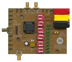
Figure 1. Evaluation Board (Top View)
© Semiconductor Components Industries, LLC, 2012
March, 2012 − Rev. 4
Surface Mount Crystal
Incorporates DIP Switch Controlled M and N Logic
Pins are Programmed on Board, Minimizing Excess
Cabling
P_Load is Push-button or Externally Controlled
Serial Input Interfaces are Accessed Externally via
SMA Connectors
Convenient and Compact Board Layout
3.3 V or 5 V Split-power Supply Operation
LVPECL/PECL Differential Output Signals are
Monitored via SMA Connectors
Figure 2. Evaluation Board (Bottom View)
1
Publication Order Number:
EVBUM2090/D
�NBC124XXEVB
LAB SET-UP PROCEDURE
Power Supply Connections and Output Termination
Dual Power Supplies
Each device has a positive supply pin, VCC, and a negative
supply pin, GND. VTT is the termination supply for the
PECL outputs, only.
Power supply terminal connectors, VCC, VTT and GND
are provided in the upper right corner of the board. The
(LV)PECL FOUT outputs must be externally DC terminated,
off the evaluation board. A “split” or dual power supply
technique can be used to take advantage of terminating the
(LV)PECL outputs into 50 � of an oscilloscope or a
frequency counter. Since VTT = VCC – 2 V, offsetting VCC
by +2 V yields VTT = 0 V or Ground. The VTT terminal
connects to the isolated SMA connector ground plane, and
is not to be confused with the device Ground pin. (see
AND8020 for more information on terminating ECL)
+2.0 V
+
VCC
+1.3 V
−
+
−
VTT
GND
+3.3V
Figure 3. “Split” or Dual Power Supply Connections
Digitial Oscilloscope
or Frequency Counter
50 �
Trigger
50 �
FOUT
FOUT
VCC = +2.0 V
J10
TEST
M[1]
M[1]
M[0]
M[0]
M[8]
M[8]
M[7]
M[7]
M[6]
M[6]
M[5]
M[5]
M[4]
M[4]
M[3]
M[3]
M[2]
M[2]
M[1]
M[1]
M[0]
M[0]
VTT = 0 V
GND = −1.3 V
SW4
VCC−8
VCC
SW3
12439
Power
J11Red − VCC
Yellow − VTT
Black − GND
ON Semiconductor
NBC12429/30/39
Evaluation Board
10338
Figure 4. “Split” or Dual Power Supply Connections
Board Layout
Table 1. “SPLIT” POWER SUPPLY CONFIGURATION
Device
Power Supply
Pin
Connector Color
VCC
GND
The evaluation board is constructed with GETEK
material and is designed to minimize noise, achieve
high bandwidth and minimize crosstalk.
SMA connectors are provided for signal access.
Serial CLOCK, Serial DATA, Serial LOAD and TEST
have SMA connector provisions, if the application requires
them.
“Spilt” Power Supply
RED
VCC = +2.0 V
YELLOW
VTT = VCC – 2 V = 0 V
BLACK
GND = −1.3 V (or –3.0 V)
http://onsemi.com
2
�NBC124XXEVB
Connect VCC banana jack to +2.0 V
Connect VTT banana jack to SMA_GND = 0 V
Connect GND banana jack to −1.3 V for 3.3 V
operation; or –3.0 V for 5 V operation
2. Ensure the oscilloscope is triggered properly and
has 50 � termination to ground. The board does
not provide 50 � source termination resistors. Two
oscilloscope trigger methods are from FOUT (using
“T” connector) or directly from FOUT.
3. Connect the (LV)PECL FOUT/FOUT outputs to the
oscilloscope with matched cables. The outputs are
terminated with 50 � to VTT (VCC – 2.0 V) = 0 V
= Ground internal to the oscilloscope.
4. Determine if a crystal (XTAL) or an external
reference (FREF_EXT) will be used. See Table 2
a) For crystal use on the 12429 or 12430, use a
crystal; no jumpers are need. For the 12439,
[M7] switch (pin 15) is set to HIGH, use a
crystal.
b)For external reference use, on the 12430 or
12439, force a logic Low on XTAL_SEL to
choose an external reference frequency.
Provide a clock input from a signal generator
(10−20 MHz) into FREF_EXT.
5. Set the programmable M and N pin switches
accordingly to achieve the desired function table
logic input levels.
6. Set the OE pin to a logic HIGH (and PWR_DWN
to a logic LOW on the 12439).
The NBC124XX evaluation board is equipped with DIP
switches, used to manipulate the static levels of the
M and N pins. The OFF (Open = “0”) condition of the DIP
switch asserts a logic LOW on the assigned pin, and the ON
(Closed = “1”) condition asserts a logic HIGH by way of the
device’s internal pull−up resistor.
Layer Stack
L1
L2
L3
L4
supply)
Signal
SMA Ground
VCC (positive power supply)
Signal/Device Ground (negative power
Lab Set−up and Measurement Procedure Getting
Started
• Equipment Used
• Agilent Signal Generator #33250A for FREF_EXT on
•
•
•
•
12430 and 12439
Tektronix TDS8000 Oscilloscope or Frequency Counter
Agilent #6624A DC Power Supply
Digital Voltmeter
Matched high−speed cables with SMA connectors
In order to get started and demonstrate the NBC124XX,
perform the following test set−up sequence:
To monitor the FOUT outputs on an oscilloscope or
frequency counter (with internal 50 � termination
impedance), the power supply needs to be DC offset:
1. Connect a “split” power supply to the evaluation
board. (see Figures 3 and 4)
VCC
JMP1
PIN 2
12430 – FREF_EXT
12439 – PWR_DOWN
JMP2
SMA J1
FREF_EXT
JMP3
PIN 3 12430 – XTAL_SEL
12439 – FREF_EXT
JMP4
GND
Figure 5. Programmable Jumpers for Device Selection and Operating Options (Pins 2 and 3, PLCC−28)
Table 2. PROGRAMMABLE JUMPER SELECTION FOR PINS 2 AND 3 (PLCC28)
12430
12439
XTAL
FREF_EXT
XTAL
FREF_EXT
PWR_DOWN
No Jumper
Use Crystal
JMP2 and JMP4
Use SMA J1
Pin 15 (M7/XTAL_SEL ⇒ High)
No Jumpers
Use Crystals
Pin 15 (M7/XTAL_SEL ⇒ Low)
JMP3
Use SMA J1
JMP1
Switch 1 − H ⇒ B 16
−L ⇒ B 1
http://onsemi.com
3
�NBC124XXEVB
EVALUATION BOARD FEATURES BY PIN
The NBC12429/430/439 Evaluation Board was designed
to accommodate the test and evaluation of all three
NBC12429/430/439 Clock Generators. Detailed board
features by device pin are described below:
OPEN. Depressing and releasing P_LOAD forces a logic
LOW-HIGH-LOW signal on the P_LOAD pin, latching the
M and N logic levels. P-LOAD also has a board trace to an
SMA connector for external control.
Crystal (XTAL1 and XTAL2)
FREF_EXT – External Reference Frequency
Either a through-hole or surface mount crystal can be
used. XTAL1 and XTAL2 have equal length board traces to
SMA connectors available to directly interface to the crystal
input pins (with an external signal source) when a zero �
resistor (or short) is placed on the board trace at the crystal
pins. Otherwise, these board traces and connectors are open
and not connected to the crystal pins and have no impedance
affect on the crystal pins.
On the 12430 and 12439, an external reference signal can
be forced into FREF_EXT via SMA J1. The XTAL_SEL pin
must set to a logic LOW. There is no 50 � resistor on this
node. If a signal generator requiring output termination is
used to drive FREF_EXT, a 50 � resistor can be added, from
the board trace or SMA conductor to the SMA ground.
FOUT and FOUT
The FOUT and FOUT PECL outputs have equal length
board traces with SMA connectors, J8 and J9. Matched
cables can connect to an oscilloscope or frequency counter.
M and N
The M and N pins are programmed by the DIP switches.
The input logic levels can be monitored by observing the
status of the appropriate LED. The M and N device pins have
internal pull-up resistors. The NBC124XX evaluation board
was designed to take advantage of this attribute. When the
M or N switch is in the logic HIGH position, the input pin
“floats” to a logic HIGH owing to the pull−up resistor and
the LED is turned ON simply for a visual indicator. A logic
HIGH voltage is not forced on the pin. In the LOW position,
the switch forces the M or N pin to the negative power supply
rail, a logic LOW. An LED power supply jumper, J11, is
provided to disable the LEDs (current). Measuring only the
device power supply current is then possible.
Serial and TEST Pins
S_CLOCK, S_DATA, S_LOAD and TEST pins have
board traces connected to SMA connectors J7, J6, J5 and J10
for external control. There are no 50 � resistors on this
nodes. If a signal sources requiring output termination are
used to drive S_CLOCK, S_DATA and S_LOAD, 50 �
resistors can be added, from the board trace or SMA
conductor to the SMA ground.
POWER_DOWN – (NBC12439)
The Power Down function on the NBC12439 can be
carried out manually by setting switch 1 A with the
condition described in Table 2 and observing the FOUT pins;
÷1 or ÷16.
P_LOAD
The P_LOAD pin “floats” to a logic HIGH by means of
the internal pull-up resistor and can be controlled manually
with the momentary push-button switch, which is normally
OE
The Output Enable function is carried out manually with
the OE switch and observing the FOUT pins.
http://onsemi.com
4
�NBC124XXEVB
Table 3. NBC12429 PIN DESCRIPTION
PIN #
PIN #
28−PLCC
32−TQFP
PIN NAME
I/O
OPEN PIN
DEFAULT
TYPE
1
4
PLL_VCC
Supply
Supply
VCC
Positive Supply for the PLL and is Connected to +3.3 V or
+5.0 V.
5
PLL_VCC
Supply
Supply
VCC
Positive Supply for the PLL and is Connected to +3.3 V or
+5.0 V.
2
3
4
5
6
6
7
8
9
10
NC
NC
XTAL1
XTAL2
OE
Input
Input
Input
Analog
Analog
CMOS/TTL
No Connect
No Connect
Crystal Oscillator Interface
Crystal Oscillator Interface
Active HIGH Output enable. The Enable is synchronous to
the Output clock to eliminate the possibility of runt pulses
on the FOUT Outputs.
7
11
P_LOAD
Input
H
CMOS/TTL
H
8
12
M0
Input
CMOS/TTL
FUNCTION
Parallel Configuration Control Input. This Pin Loads the
Configuration Latches with the contents of the parallel Inputs. The Latches will be transparent when the signal is
LOW; therefore, the parallel data must be stable on the
LOW−to−HIGH transition of P_LOAD for proper operation.
Used to configure the PLL loop divider. Sampled on the
LOW−to−HIGH transition of P_LOAD. M0 is the LSB.
9
13
M1
Input
H
H
10
14
M2
Input
H
CMOS/TTL
Used to configure the PLL loop divider. Sampled on the
LOW−to−HIGH transition of P_LOAD.
11
15
M3
Input
H
CMOS/TTL
Used to configure the PLL loop divider. Sampled on the
LOW−to−HIGH transition of P_LOAD.
12
16
17
NC
M4
Input
H
H
CMOS/TTL
13
18
M5
Input
H
CMOS/TTL
Used to configure the PLL loop divider. Sampled on the
LOW−to−HIGH transition of P_LOAD.
14
19
M6
Input
H
CMOS/TTL
Used to configure the PLL loop divider. Sampled on the
LOW−to−HIGH transition of P_LOAD.
15
20
M7
Input
H
CMOS/TTL
Used to configure the PLL loop divider. Sampled on the
LOW−to−HIGH transition of P_LOAD.
16
21
M8
Input
CMOS/TTL
Used to configure the PLL loop divider. Sampled on the
LOW−to−HIGH transition of P_LOAD. M8 is the MSB.
CMOS/TTL
Output divider Input. Used to configure the Output divider
modules. Sampled on the LOW−to−HIGH transition of
P_LOAD.
Output divider Input. Used to configure the Output divider
modules. Sampled on the LOW−to−HIGH transition of
P_LOAD.
No Connect
Negative Power Supply (GND)
Test and device diagnostics Output; function is determined
by serial Configuration bits T[2:0].
CMOS/TTL
Used to configure the PLL loop divider. Sampled on the
LOW−to−HIGH transition of P_LOAD.
H
17
22
N0
Input
H
18
23
N1
Input
CMOS/TTL
H
No Connect
Used to configure the PLL loop divider. Sampled on the
LOW−to−HIGH transition of P_LOAD.
19
20
24
25
26
NC
GND
TEST
Supply
Output
Supply
Ground
CMOS/TTL
21
27
VCC
Supply
Supply
VCC
Positive Supply for the internal logic and Output buffers,
and is Connected to +3.3 V or +5.0 V.
28
VCC
Supply
Supply
VCC
Positive Supply for the internal logic and Output buffers,
and is Connected to +3.3 V or +5.0 V.
22
23
24
25
29
30
31
32
GND
FOUT
FOUT
VCC
Supply
Output
Output
Supply
Supply
Supply
Ground
PECL
PECL
VCC
Negative Power Supply (GND)
Differential Clock Output
Differential Clock Output
Positive Supply for the internal logic and Output buffers,
and is Connected to +3.3 V or +5.0 V.
26
27
28
1
2
3
S_CLOCK
S_DATA
S_LOAD
Input
Input
Input
L
L
L
CMOS/TTL
CMOS/TTL
CMOS/TTL
Clock Input to the serial Configuration shift registers
Data Input to the serial Configuration shift registers
Load Input, which Latches the contents of the shift, registers. The Latches will be transparent when this signal is
HIGH; thus, the data must be stable on the HIGH−to−LOW
transition of S_LOAD for proper operation.
http://onsemi.com
5
�NBC124XXEVB
Table 4. NBC12430 PIN DESCRIPTION
PIN
28−PLCC 32−TQFP
1
4
Pin Name
PLL_VCC
I/O
Supply
Open Pin
Default
Supply
TYPE
VCC
FUNCTION
Positive Supply for the PLL and is Connected to +3.3 V or
+5.0 V.
5
PLL_VCC
Supply
Supply
VCC
Positive Supply for the PLL and is Connected to +3.3 V or
+5.0 V.
2
3
6
7
FREF_EXT
XTAL_SEL
Input
Input
L
H
4
5
6
8
9
10
XTAL1
XTAL2
OE
Input
Input
Input
7
11
P_LOAD
Input
H
External PLL reference frequency
Selects between the crystal and the FREF_EXT source for
the PLL
Analog
Analog
CMOS/TTL
Crystal Oscillator Interface
Crystal Oscillator Interface
Active HIGH Output enable. The Enable is synchronous to
the Output clock to eliminate the possibility of runt pulses on
the FOUT Outputs.
CMOS/TTL
Parallel Configuration Control Input. This Pin Loads the Configuration Latches with the contents of the parallel Inputs. The
Latches will be transparent when the signal is LOW; therefore, the parallel data must be stable on the LOW−to−HIGH
transition of P_LOAD for proper operation.
Used to configure the PLL loop divider. Sampled on the
LOW−to−HIGH transition of P_LOAD. M0 is the LSB.
H
8
12
M0
Input
CMOS/TTL
9
13
M1
Input
H
H
10
14
M2
Input
H
CMOS/TTL
Used to configure the PLL loop divider. Sampled on the
LOW−to−HIGH transition of P_LOAD.
11
15
M3
Input
H
CMOS/TTL
Used to configure the PLL loop divider. Sampled on the
LOW−to−HIGH transition of P_LOAD.
12
16
17
NC
M4
Input
H
H
CMOS/TTL
13
18
M5
Input
H
CMOS/TTL
Used to configure the PLL loop divider. Sampled on the
LOW−to−HIGH transition of P_LOAD.
14
19
M6
Input
H
CMOS/TTL
Used to configure the PLL loop divider. Sampled on the
LOW−to−HIGH transition of P_LOAD.
15
20
M7
Input
H
CMOS/TTL
Used to configure the PLL loop divider. Sampled on the
LOW−to−HIGH transition of P_LOAD.
16
21
M8
Input
CMOS/TTL
Used to configure the PLL loop divider. Sampled on the
LOW−to−HIGH transition of P_LOAD. M8 is the MSB.
CMOS/TTL
Output divider Input. Used to configure the Output divider
modules. Sampled on the LOW−to−HIGH transition of
P_LOAD.
Output divider Input. Used to configure the Output divider
modules. Sampled on the LOW−to−HIGH transition of
P_LOAD.
No Connect
Negative Power Supply (GND)
Test and device diagnostics Output; function is determined by
serial Configuration bits T[2:0].
CMOS/TTL
Used to configure the PLL loop divider. Sampled on the
LOW−to−HIGH transition of P_LOAD.
H
17
22
N0
Input
H
18
23
N1
Input
CMOS/TTL
H
No Connect
Used to configure the PLL loop divider. Sampled on the
LOW−to−HIGH transition of P_LOAD.
19
20
24
25
26
NC
GND
TEST
Supply
Output
Supply
Ground
CMOS/TTL
21
27
VCC
Supply
Supply
VCC
Positive Supply for the internal logic and Output buffers, and
is Connected to +3.3 V or +5.0 V.
28
VCC
Supply
Supply
VCC
Positive Supply for the internal logic and Output buffers, and
is Connected to +3.3 V or +5.0 V.
22
23
24
25
29
30
31
32
GND
FOUT
FOUT
VCC
Supply
Output
Output
Supply
Supply
Supply
Ground
PECL
PECL
VCC
Negative Power Supply (GND)
Differential Clock Output
Differential Clock Output
Positive Supply for the internal logic and Output buffers, and
is Connected to +3.3 V or +5.0 V.
26
27
28
1
2
3
S_CLOCK
S_DATA
S_LOAD
Input
Input
Input
L
L
L
CMOS/TTL
CMOS/TTL
CMOS/TTL
Clock Input to the serial Configuration shift registers
Data Input to the serial Configuration shift registers
Load Input, which Latches the contents of the shift, registers.
The Latches will be transparent when this signal is HIGH;
thus, the data must be stable on the HIGH−to−LOW transition
of S_LOAD for proper operation.
http://onsemi.com
6
�NBC124XXEVB
Table 5. NBC12439 PIN DESCRIPTION
PIN #
PIN #
28−PLCC
32−TQFP
PIN NAME
I/O
OPEN PIN
DEFAULT
TYPE
FUNCTION
1
4
PLL_VCC
Supply
Supply
VCC
Positive Supply for the PLL and is Connected to +3.3 V or
+5.0 V.
5
PLL_VCC
Supply
Supply
VCC
Positive Supply for the PLL and is Connected to +3.3 V or
+5.0 V.
2
6
PWR_DO
WN
Input
L
3
4
5
6
7
8
9
10
FREF_EXT
XTAL1
XTAL2
OE
Input
Input
Input
Input
L
7
11
P_LOAD
Input
Forces the FOUT Outputs to synchronously reduce its frequency by a factor of 16
Analog
Analog
CMOS/TTL
H
CMOS/TTL
H
8
12
M0
Input
CMOS/TTL
External PLL reference frequency
Crystal Oscillator Interface
Crystal Oscillator Interface
Active HIGH Output enable. The Enable is synchronous to
the Output clock to eliminate the possibility of runt pulses
on the FOUT Outputs.
Parallel Configuration Control Input. This Pin Loads the
Configuration Latches with the contents of the parallel
Inputs. The Latches will be transparent when the signal is
LOW; therefore, the parallel data must be stable on the
LOW−to−HIGH transition of P_LOAD for proper operation.
Used to configure the PLL loop divider. Sampled on the
LOW−to−HIGH transition of P_LOAD. M0 is the LSB.
9
13
M1
Input
H
H
10
14
M2
Input
H
CMOS/TTL
Used to configure the PLL loop divider. Sampled on the
LOW−to−HIGH transition of P_LOAD.
11
15
M3
Input
H
CMOS/TTL
Used to configure the PLL loop divider. Sampled on the
LOW−to−HIGH transition of P_LOAD.
12
16
17
NC
M4
Input
H
H
CMOS/TTL
13
18
M5
Input
H
CMOS/TTL
Used to configure the PLL loop divider. Sampled on the
LOW−to−HIGH transition of P_LOAD.
14
19
M6
Input
H
CMOS/TTL
Used to configure the PLL loop divider. Sampled on the
LOW−to−HIGH transition of P_LOAD.
15
20
XTAL_SEL
Input
H
CMOS/TTL
Selects between the crystal and the FREF_EXT source for
the PLL
16
17
21
22
NC
N0
Input
CMOS/TTL
Used to configure the PLL loop divider. Sampled on the
LOW−to−HIGH transition of P_LOAD.
CMOS/TTL
H
18
23
N1
Input
CMOS/TTL
H
No Connect
Used to configure the PLL loop divider. Sampled on the
LOW−to−HIGH transition of P_LOAD.
No Connect
Output divider Input. Used to configure the Output divider
modulus. Sampled on the LOW−to−HIGH transition of
P_LOAD.
Output divider Input. Used to configure the Output divider
modulus. Sampled on the LOW−to−HIGH transition of
P_LOAD.
No Connect
Negative Power Supply (GND)
Test and device diagnostics Output; function is determined
by serial Configuration bits T[2:0].
19
20
24
25
26
NC
GND
TEST
Supply
Output
Supply
Ground
CMOS/TTL
21
27
VCC
Supply
Supply
VCC
Positive Supply for the internal logic and Output buffers,
and is Connected to +3.3 V or +5.0 V.
28
VCC
Supply
Supply
VCC
Positive Supply for the internal logic and Output buffers,
and is Connected to +3.3 V or +5.0 V.
22
23
24
25
29
30
31
32
GND
FOUT
FOUT
VCC
Supply
Output
Output
Supply
Supply
Supply
Ground
PECL
PECL
VCC
Negative Power Supply (GND)
Differential Clock Output
Differential Clock Output
Positive Supply for the internal logic and Output buffers,
and is Connected to +3.3 V or +5.0 V.
26
27
28
1
2
3
S_CLOCK
S_DATA
S_LOAD
Input
Input
Input
L
L
L
CMOS/TTL
CMOS/TTL
CMOS/TTL
Clock Input to the serial Configuration shift registers
Data Input to the serial Configuration shift registers
Load Input, which Latches the contents of the shift, registers. The Latches will be transparent when this signal is
HIGH; thus, the data must be stable on the HIGH−to−LOW
transition of S_LOAD for proper operation.
http://onsemi.com
7
�NBC124XXEVB
Table 6. NBC12429/12430/12439 PACKAGE PIN DESCRIPTION
PKG PIN #
PKG PIN #
28−PLCC
12429
12430
12439
32−LQFP
12429
12430
12439
1
VCC−PLL
VCC−PLL
VCC−PLL
1
SCLOCK
SCLOCK
SCLOCK
2
NC
FREF_EXT
PWR_DOWN
2
SDATA
SDATA
SDATA
3
NC
XTAL_SEL
FREF_EXT
3
SLOAD
SLOAD
SLOAD
4
XTAL1
XTAL1
XTAL1
4
VCC_PLL
VCC_PLL
VCC_PLL
5
XTAL2
XTAL2
XTAL2
5
VCC_PLL
VCC_PLL
VCC_PLL
6
OE
OE
OE
6
NC
FREF_EXT
PWR_DOWN
7
P_LOAD
P_LOAD
P_LOAD
7
NC
XTAL_SEL
FREF_EXT
8
M0
M0
M0
8
XTAL1
XTAL1
XTAL1
9
M1
M1
M1
9
XTAL2
XTAL2
XTAL2
10
M2
M2
M2
10
OE
OE
OE
11
M3
M3
M3
11
P_LOAD
P_LOAD
P_LOAD
12
M4
M4
M4
12
M0
M0
M0
13
M5
M5
M5
13
M1
M1
M1
14
M6
M6
M6
14
M2
M2
M2
15
M7
M7
XTAL_SEL
15
M3
M3
M2
16
M8
M8
NC
16
NC
NC
NC
17
N0
N0
N0
17
M4
M4
M4
18
N1
N1
N1
18
M5
M5
M5
19
GND
GND
GND
19
M6
M6
M6
20
TEST
TEST
TEST
20
M7
M7
XTAL_SEL
21
VCC
VCC
VCC
21
M8
M8
NC
22
GND
GND
GND
22
N0
N0
N0
23
FOUT
FOUT
FOUT
23
N1
N1
N1
24
FOUT
FOUT
FOUT
24
NC
NC
NC
25
VCC
VCC
VCC
25
GND
GND
GND
26
SCLOCK
SCLOCK
SCLOCK
26
TEST
TEST
TEST
27
SDATA
SDATA
SDATA
27
VCC
VCC
VCC
28
SLOAD
SLOAD
SLOAD
28
VCC
VCC
VCC
29
GND
GND
GND
30
FOUT
FOUT
FOUT
31
FOUT
FOUT
FOUT
32
VCC
VCC
VCC
http://onsemi.com
8
�NBC124XXEVB
Table 7. BILL OF MATERIAL
Designator
Qty
J8,J9,J1,J4
4
Connector
Component
SMA Jack, Edge Mount, Johnson Comp Inc.
#142−0701−801
Description
Digikey #
Vendor PN
J502−ND
142−0701−801
C5,C7,C3,C
6,C8,C11,
C14
7
Capacitor
chip, 0.010 �F, 0805, AVX #08055C103KAT2A
478−1383−1−ND
08055C103KAT2A
C10,C13
2
Capacitor
chip, 0.1 �F, 0805, Panasonic
#ECJ−2YB1H104K
PCC1840CT−ND
ECJ−2YB1H104K
C9,C12,C4
3
Capacitor
chip, 22 �F, Tant ”D”, Kemet, T494D226K016AS
399−1782−1−ND
T494D226K016AS
R4−F14
1
Header
Double Row, Male, Sullens, #PTC18DAAN
S2012−18−ND
PTC18DAAN
11
Resistor
Chip, 330 �, 0805, Panasonic
#ERJ−6GEYJ331V
P330ACT−ND
ERJ−6GEYJ331V
R2
1
Resistor
Chip, 13.3 �, 0805, Panasonic
#ERJ−6ENF13R3V
P13.3CCT−ND
ERJ−6ENF13R3V
SW1
1
Switch
SPST, GULL, Sealed, Grayhill #90HBW02P
GH1291−ND
90HBW02P
SW2,SW3,
SW4
3
Switch
SPDT, Toggle, 4 Stations, Grayhill #76STC04
N0,N1
1
Switch
SPST, Momentary, Push Button, Omron
#B3S−1002
SW416−ND
B3S−1002
M0−M8
2
LED
Diffused, Amber, Lumex #SSL−LX2573AD
67−1045−ND
SSL−LX2573AD
XTAL1 & 2
9
LED
Diffused, Green, Lumex #SSL−LX2573GD
67−1046−ND
SSL−LX2573GD
2
Pin Recepicle
(For Through−Hole Crystal), Mill−Max
#M0462−0−15−15−11−14−04−0
1
Crystal
16.000 MHz, Series
Through−Hole
Surface Mount
X1008−ND
XC983CT−ND
ECS−160−5−1X
ECS−160−5−23A−EN−TR
76STC04
VCC
1
Red Side Launch Banana Jack
DELTRON 571−0500
DUGND
1
Black Side Launch Banana Jack
DELTRON 571−0100
SMAGND
1
Yellow Side Launch Banana Jack
DELTRON 571−0700
http://onsemi.com
9
�11338.sch−1 − Thu Feb 06 07:08:11 2003
10
http://onsemi.com
Anode
Anode
Anode
Anode
Anode
Anode
Anode
Anode
Anode
Anode
NBC124XXEVB
�onsemi,
, and other names, marks, and brands are registered and/or common law trademarks of Semiconductor Components Industries, LLC dba “onsemi” or its affiliates
and/or subsidiaries in the United States and/or other countries. onsemi owns the rights to a number of patents, trademarks, copyrights, trade secrets, and other intellectual property. A
listing of onsemi’s product/patent coverage may be accessed at www.onsemi.com/site/pdf/Patent−Marking.pdf. onsemi is an Equal Opportunity/Affirmative Action Employer. This
literature is subject to all applicable copyright laws and is not for resale in any manner.
The evaluation board/kit (research and development board/kit) (hereinafter the “board”) is not a finished product and is not available for sale to consumers. The board is only intended
for research, development, demonstration and evaluation purposes and will only be used in laboratory/development areas by persons with an engineering/technical training and familiar
with the risks associated with handling electrical/mechanical components, systems and subsystems. This person assumes full responsibility/liability for proper and safe handling. Any
other use, resale or redistribution for any other purpose is strictly prohibited.
THE BOARD IS PROVIDED BY ONSEMI TO YOU “AS IS” AND WITHOUT ANY REPRESENTATIONS OR WARRANTIES WHATSOEVER. WITHOUT LIMITING THE FOREGOING,
ONSEMI (AND ITS LICENSORS/SUPPLIERS) HEREBY DISCLAIMS ANY AND ALL REPRESENTATIONS AND WARRANTIES IN RELATION TO THE BOARD, ANY
MODIFICATIONS, OR THIS AGREEMENT, WHETHER EXPRESS, IMPLIED, STATUTORY OR OTHERWISE, INCLUDING WITHOUT LIMITATION ANY AND ALL
REPRESENTATIONS AND WARRANTIES OF MERCHANTABILITY, FITNESS FOR A PARTICULAR PURPOSE, TITLE, NON−INFRINGEMENT, AND THOSE ARISING FROM A
COURSE OF DEALING, TRADE USAGE, TRADE CUSTOM OR TRADE PRACTICE.
onsemi reserves the right to make changes without further notice to any board.
You are responsible for determining whether the board will be suitable for your intended use or application or will achieve your intended results. Prior to using or distributing any systems
that have been evaluated, designed or tested using the board, you agree to test and validate your design to confirm the functionality for your application. Any technical, applications or
design information or advice, quality characterization, reliability data or other services provided by onsemi shall not constitute any representation or warranty by onsemi, and no additional
obligations or liabilities shall arise from onsemi having provided such information or services.
onsemi products including the boards are not designed, intended, or authorized for use in life support systems, or any FDA Class 3 medical devices or medical devices with a similar
or equivalent classification in a foreign jurisdiction, or any devices intended for implantation in the human body. You agree to indemnify, defend and hold harmless onsemi, its directors,
officers, employees, representatives, agents, subsidiaries, affiliates, distributors, and assigns, against any and all liabilities, losses, costs, damages, judgments, and expenses, arising
out of any claim, demand, investigation, lawsuit, regulatory action or cause of action arising out of or associated with any unauthorized use, even if such claim alleges that onsemi was
negligent regarding the design or manufacture of any products and/or the board.
This evaluation board/kit does not fall within the scope of the European Union directives regarding electromagnetic compatibility, restricted substances (RoHS), recycling (WEEE), FCC,
CE or UL, and may not meet the technical requirements of these or other related directives.
FCC WARNING – This evaluation board/kit is intended for use for engineering development, demonstration, or evaluation purposes only and is not considered by onsemi to be a finished
end product fit for general consumer use. It may generate, use, or radiate radio frequency energy and has not been tested for compliance with the limits of computing devices pursuant
to part 15 of FCC rules, which are designed to provide reasonable protection against radio frequency interference. Operation of this equipment may cause interference with radio
communications, in which case the user shall be responsible, at its expense, to take whatever measures may be required to correct this interference.
onsemi does not convey any license under its patent rights nor the rights of others.
LIMITATIONS OF LIABILITY: onsemi shall not be liable for any special, consequential, incidental, indirect or punitive damages, including, but not limited to the costs of requalification,
delay, loss of profits or goodwill, arising out of or in connection with the board, even if onsemi is advised of the possibility of such damages. In no event shall onsemi’s aggregate liability
from any obligation arising out of or in connection with the board, under any theory of liability, exceed the purchase price paid for the board, if any.
The board is provided to you subject to the license and other terms per onsemi’s standard terms and conditions of sale. For more information and documentation, please visit
www.onsemi.com.
PUBLICATION ORDERING INFORMATION
LITERATURE FULFILLMENT:
Email Requests to: orderlit@onsemi.com
onsemi Website: www.onsemi.com
◊
TECHNICAL SUPPORT
North American Technical Support:
Voice Mail: 1 800−282−9855 Toll Free USA/Canada
Phone: 011 421 33 790 2910
www.onsemi.com
1
Europe, Middle East and Africa Technical Support:
Phone: 00421 33 790 2910
For additional information, please contact your local Sales Representative
�