Is Now Part of
To learn more about ON Semiconductor, please visit our website at
www.onsemi.com
Please note: As part of the Fairchild Semiconductor integration, some of the Fairchild orderable part numbers
will need to change in order to meet ON Semiconductor’s system requirements. Since the ON Semiconductor
product management systems do not have the ability to manage part nomenclature that utilizes an underscore
(_), the underscore (_) in the Fairchild part numbers will be changed to a dash (-). This document may contain
device numbers with an underscore (_). Please check the ON Semiconductor website to verify the updated
device numbers. The most current and up-to-date ordering information can be found at www.onsemi.com. Please
email any questions regarding the system integration to Fairchild_questions@onsemi.com.
ON Semiconductor and the ON Semiconductor logo are trademarks of Semiconductor Components Industries, LLC dba ON Semiconductor or its subsidiaries in the United States and/or other countries. ON Semiconductor owns the rights to a number
of patents, trademarks, copyrights, trade secrets, and other intellectual property. A listing of ON Semiconductor’s product/patent coverage may be accessed at www.onsemi.com/site/pdf/Patent-Marking.pdf. ON Semiconductor reserves the right
to make changes without further notice to any products herein. ON Semiconductor makes no warranty, representation or guarantee regarding the suitability of its products for any particular purpose, nor does ON Semiconductor assume any liability
arising out of the application or use of any product or circuit, and specifically disclaims any and all liability, including without limitation special, consequential or incidental damages. Buyer is responsible for its products and applications using ON
Semiconductor products, including compliance with all laws, regulations and safety requirements or standards, regardless of any support or applications information provided by ON Semiconductor. “Typical” parameters which may be provided in ON
Semiconductor data sheets and/or specifications can and do vary in different applications and actual performance may vary over time. All operating parameters, including “Typicals” must be validated for each customer application by customer’s
technical experts. ON Semiconductor does not convey any license under its patent rights nor the rights of others. ON Semiconductor products are not designed, intended, or authorized for use as a critical component in life support systems or any FDA
Class 3 medical devices or medical devices with a same or similar classification in a foreign jurisdiction or any devices intended for implantation in the human body. Should Buyer purchase or use ON Semiconductor products for any such unintended
or unauthorized application, Buyer shall indemnify and hold ON Semiconductor and its officers, employees, subsidiaries, affiliates, and distributors harmless against all claims, costs, damages, and expenses, and reasonable attorney fees arising out
of, directly or indirectly, any claim of personal injury or death associated with such unintended or unauthorized use, even if such claim alleges that ON Semiconductor was negligent regarding the design or manufacture of the part. ON Semiconductor
is an Equal Opportunity/Affirmative Action Employer. This literature is subject to all applicable copyright laws and is not for resale in any manner.
�Revised October 2004
NC7SZ374
TinyLogic UHS D-Type Flip-Flop with 3-STATE Output
General Description
Features
The NC7SZ374 is a single positive edge-triggered D-type
CMOS Flip-Flop with 3-STATE output from Fairchild’s Ultra
High Speed Series of TinyLogic in the space saving
SC70 6-lead package. The device is fabricated with
advanced CMOS technology to achieve ultra high speed
with high output drive while maintaining low static power
dissipation over a very broad VCC operating range. The
device is specified to operate over the 1.65V to 5.5V VCC
range. The inputs and output are high impedance when
VCC is 0V. Inputs tolerate voltages up to 7V independent of
VCC operating voltage. This single flip-flop will store the
state of the D input that meets the setup and hold time
requirements on the LOW-to-HIGH Clock (CP) transition.
The output tolerates voltages above VCC in the 3-STATE
condition.
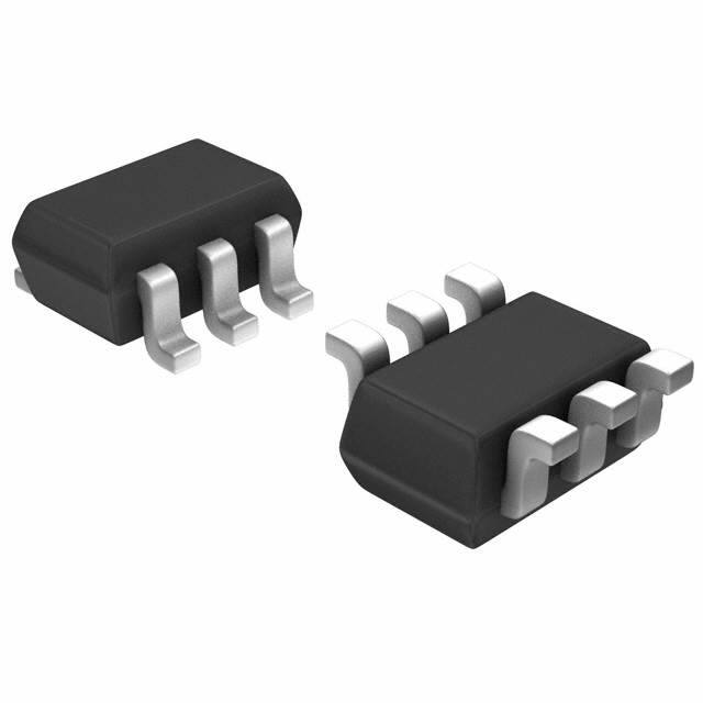
■ Space saving SC70 6-lead package
■ Ultra small MicroPak leadless package
■ Ultra High Speed; tPD 2.6 ns Typ into 50 pF at 5V VCC
■ High Output Drive; ±24 mA at 3V VCC
■ Broad VCC Operating Range; 1.65V to 5.5V
■ Matches the performance of LCX when operated at
3.3V VCC
■ Power down high impedance inputs/output
■ Overvoltage tolerant inputs facilitate 5V - 3V translation
■ Patented noise/EMI reduction circuitry implemented
Ordering Code:
Order
Package
Product Code
Number
Number
Top Mark
NC7SZ374P6X
MAA06A
Z74
6-Lead SC70, EIAJ SC88, 1.25mm Wide
3k Units on Tape and Reel
NC7SZ374L6X
MAC06A
C9
6-Lead MicroPak, 1.0mm Wide
5k Units on Tape and Reel
Package Description
Supplied As
TinyLogic is a registered trademark of Fairchild Semiconductor Corporation.
MicroPak is a trademark of Fairchild Semiconductor Corporation.
© 2004 Fairchild Semiconductor Corporation
DS500156
www.fairchildsemi.com
NC7SZ374 TinyLogic UHS D-Type Flip-Flop with 3-STATE Output
May 1998
�NC7SZ374
Logic Symbol
Connection Diagrams
IEEE/IEC
Pin Assignments for SC70
Pin Descriptions
Pin Names
Description
D
Data Input
CP
Clock Pulse Input
OE
Output Enable Input
Q
Flip-Flop Output
(Top View)
Pin One Orientation Diagram
Function Table
Inputs
�
�
�
CP
D
X
H = HIGH Logic Level
L = LOW Logic Level
AAA represents Product Code Top Mark - see ordering code
Output
OE
Note: Orientation of Top Mark determines Pin One location. Read the top
product code mark left to right, Pin One is the lower left pin (see diagram).
Q
L
L
L
H
L
H
X
L
Qn
X
H
Z
Pad Assignment for MicroPak
Z = High Impedance
X = Immaterial
Qn = No change in data
(Top Thru View)
www.fairchildsemi.com
2
�Supply Voltage (VCC)
−0.5V to +7.0V
DC Input Voltage (VIN)
−0.5V to +7.0V
DC Output Voltage (VOUT)
−0.5V to +7.0V
Recommended Operating
Conditions (Note 2)
Power Supply
DC Input Diode Current (IIK)
VIN < 0V
−50 mA
Operating (VCC )
1.65V to 5.5V
Data Retention
1.5V to 5.5V
Input Voltage (VIN)
DC Output Diode Current (IOK)
0V to 5.5V
Output Voltage (VOUT)
VOUT < 0V
DC Output (IOUT) Source/Sink Current
−50 mA
Active State
0V to VCC
± 50 mA
3-STATE
0V to 5.5V
± 50 mA
DC VCC/GND Current (ICC/IGND)
Input Rise and Fall Time (tr, tf)
−65°C to +150°C
Storage Temperature Range (TSTG)
150°C
Junction Temperature under Bias (TJ)
VCC = 1.8V, 2.5V ± 0.2V
0 to 20 ns/V
VCC = 3.3V ± 0.3V
0 to 10 ns/V
VCC = 5.5V ± 0.5V
Junction Lead Temperature (TL)
260°C
(Soldering, 10 seconds)
Power Dissipation (PD) @ +85°C
0 to 5 ns/V
−40°C to +85°C
Operating Temperature (TA)
Thermal Resistance (θJA)
180 mW
350° C/W
Note 1: Absolute Maximum Ratings: are those values beyond which the
safety of the device cannot be guaranteed. The device should not be operated at these limits. The parametric values defined in the Electrical Characteristics tables are not guaranteed at the absolute maximum ratings. The
“Recommended Operating Conditions” table will define the conditions for
actual device operation.
Note 2: Unused inputs must be held HIGH or LOW. They may not float.
DC Electrical Characteristics
Symbol
VIH
Parameter
HIGH Level Control
Input Voltage
VIL
LOW Level Control
Input Voltage
VOH
HIGH Level Control
Output Voltage
VOL
VCC
TA = +25°C
(V)
Min
TA = −40°C to +85°C
Typ
Max
1.65 to 1.95 0.75 VCC
2.3 to 5.5
2.3 to 5.5
0.25 VCC
0.3 VCC
1.65
0.3 VCC
1.8
1.7
1.8
1.7
2.3
2.2
2.3
2.2
3.0
2.9
3.0
2.9
4.5
4.4
4.5
4.4
1.65
1.24
1.52
1.29
2.3
1.9
2.15
1.9
3.0
2.4
2.8
2.4
IOH = −16 mA
3.0
2.3
2.68
2.3
IOH = −24 mA
4.5
3.8
4.2
V
0.1
Output Voltage
1.8
0.0
0.1
0.1
2.3
0.0
0.1
0.1
3.0
0.0
0.1
0.1
IOFF
Power Off Leakage Current
ICC
Quiescent Supply Current
IOH = −4 mA
IOH = −32 mA
3.8
0.1
3-STATE Output Leakage
VIN = VIH
IOH = −8 mA
0.0
IOZ
V
IOH = −100 µA
1.65
Input Leakage Current
Conditions
1.55
LOW Level Control
IIN
Units
V
0.7 VCC
0.25 VCC
1.55
Max
0.75 VCC
0.75 VCC
1.65 to 1.95
1.65
Min
IOL = 100 µA
4.5
0.0
0.1
0.1
1.65
0.08
0.24
0.24
2.3
0.10
0.3
0.3
IOL = 8 mA
3.0
0.15
0.4
0.4
IOL = 16 mA
3.0
0.22
0.55
0.55
IOL = 24 mA
4.5
0.22
0.55
0.55
0 to 5.5
±0.1
±1.0
µA
0 ≤ VIN ≤ 5.5V
1.65 to 5.5
±0.5
±5.0
µA
VIN = VIL or VIH
0.0
1.0
10
µA
VIN or VOUT = 5.5V
1.65 to 5.5
1.0
10.0
µA
VIN = 5.5V, GND
V
VIN = VIH
IOL = 4 mA
IOL = 32 mA
0 ≤ VOUT ≤ 5.5V
3
www.fairchildsemi.com
NC7SZ374
Absolute Maximum Ratings(Note 1)
�NC7SZ374
AC Electrical Characteristics
Symbol
fMAX
VCC
(V)
Parameter
TA = +25°C
Min
Typ
TA = −40°C to +85°C
Max
Min
Maximum Clock
1.65
100
Frequency
1.8
100
2.5 ± 0.2
125
3.3 ± 0.3
150
5.0 ± 0.5
tPLH
Propagation Delay
tPHL
CP to Q
tPLZ
tH
RD = 500Ω, S1 = Open
Figure
Number
Figures
1, 3
175
1.50
2.5
16.5
1.8
2.5
6.5
10.0
2.5
11.0
2.5 ± 0.2
2.0
3.8
6.5
2.0
7.0
3.3 ± 0.3
1.5
2.8
4.5
1.4
5.0
5.0 ± 0.5
1.0
2.2
3.5
1.0
3.8
3.3 ± 0.3
2.0
3.4
5.5
1.6
6.2
CL = 50 pF
5.0 ± 0.5
1.5
2.6
4.0
1.4
4.7
RD = 500 Ω, S1 = Open
1.65
2.0
9.0
13.5
2.0
14.3
1.8
2.0
6.0
9.0
2.0
9.5
2.5 ± 0.2
2.0
3.7
6.0
1.8
6.6
3.3 ± 0.3
1.5
2.8
5.0
1.4
5.3
S1 = GND for tPZH
5.0 ± 0.5
1.0
2.2
3.7
1.0
3.9
S1 = VI for tPZL
1.65
2.0
7.7
12.0
2.0
13.0
CL = 15 pF
ns
RD = 1 MΩ
CL = 50 pF, VI = 2x VCC
ns
RU, RD = 500 Ω
CL = 50 pF, VI = 2x VCC
1.8
2.0
5.1
8.0
2.0
8.5
2.0
3.5
6.0
1.8
6.3
3.3 ± 0.3
1.5
2.8
4.5
1.4
4.7
S1 = GND for tPHZ
5.0 ± 0.5
1.0
2.3
3.7
1.0
3.9
S1 = VI for tPLZ
2.5 ± 0.2
2.5
CP to D
3.3 ± 0.3
2.0
5.0 ± 0.5
1.5
Hold Time,
2.5 ± 0.2
1.5
CP to D
3.3 ± 0.3
1.5
5.0 ± 0.5
1.5
2.5 ± 0.2
3.0
3.3 ± 0.3
2.8
5.0 ± 0.5
2.5
Figures
1, 3
S1 = Open
2.5 ± 0.2
Setup Time,
Pulse Width, CP
tW
CL = 50 pF
9.7
Output Disable Time
tS
MHz
Conditions
2.5
tPZH
tPHZ
Units
1.65
Output Enable Time
tPZL
Max
ns
RU, RD = 500 Ω
CL = 50 pF
ns
RD = 500 Ω, S1 = Open
CL = 50 pF
ns
D
= 500 Ω, S1 = Open
Figures
1, 3
Figures
1, 4
Figures
1, 4
Figures
1, 5
Figures
1, 5
CL = 50 pF
ns
RD = 500 Ω, S1 = Open
Figures
1, 5
Capacitance (Note 3)
Symbol
Parameter
Typ
Max
Units
Conditions
3
pF
VCC = Open, VIN 0V or VCC
Output Capacitance
4
pF
VCC = 3.3V, VIN = 0V or VCC
Power Dissipation Capacitance (Note 4)
10
CIN
Input Capacitance
COUT
CPD
12
pF
VCC = 3.3V
VCC = 5.0V
Note 3: TA = +25C, f = 1MHz.
Note 4: C PD is defined as the value of the internal equivalent capacitance which is derived from dynamic operating current consumption (ICCD ) at no output
loading and operating at 50% duty cycle. (See Figure 2) CPD is related to ICCD dynamic operating current by the expression:
ICCD = (CPD) (VCC) (fIN) + (ICCstatic).
www.fairchildsemi.com
4
�NC7SZ374
AC Loading and Waveforms
CL includes load and stray capacitance
CP Input = AC Waveform; tr = tf = 1.8 ns;
Input PRR = 1.0 MHz; tw = 500 ns
CP Input PRR = 10 MHz; Duty Cycle = 50%
D Input PRR = 5MHz; Duty Cycle = 50%
FIGURE 1. AC Test Circuit
FIGURE 2. ICCD Test Circuit
FIGURE 3. AC Waveforms
FIGURE 4. AC Waveforms
FIGURE 5. AC Waveforms
5
www.fairchildsemi.com
�NC7SZ374
Tape and Reel Specification
TAPE FORMAT for SC70
Package
Designator
P6X
Tape
Number
Cavity
Section
Cavities
Status
Cover Tape
Status
Leader (Start End)
125 (typ)
Empty
Sealed
Carrier
3000
Filled
Sealed
Trailer (Hub End)
75 (typ)
Empty
Sealed
TAPE DIMENSIONS inches (millimeters)
Package
SC70-6
Tape Size
8 mm
www.fairchildsemi.com
DIM A
DIM B
0.093
0.096
(2.35)
(2.45)
DIM F
DIM Ko
0.138 ± 0.004 0.053 ± 0.004
(3.5 ± 0.10)
6
(1.35 ± 0.10)
DIM P1
DIM W
0.157
0.315 ± 0.004
(4)
(8 ± 0.1)
�TAPE FORMAT for MicroPak
Package
Designator
(Continued)
Tape
Number
Cavity
Section
Cavities
Status
Status
Leader (Start End)
125 (typ)
Empty
Sealed
L6X
Cover Tape
Carrier
5000
Filled
Sealed
Trailer (Hub End)
75 (typ)
Empty
Sealed
N
W1
W2
W3
REEL DIMENSIONS inches (millimeters)
Tape
Size
8 mm
A
B
C
D
7.0
0.059
0.512
0.795
2.165
0.331 + 0.059/−0.000
0.567
W1 + 0.078/−0.039
(177.8)
(1.50)
(13.00)
(20.20)
(55.00)
(8.40 + 1.50/−0.00)
(14.40)
(W1 + 2.00/−1.00)
7
www.fairchildsemi.com
NC7SZ374
Tape and Reel Specification
�NC7SZ374
Physical Dimensions inches (millimeters) unless otherwise noted
6-Lead SC70, EIAJ SC88, 1.25mm Wide
Package Number MAA06A
www.fairchildsemi.com
8
�NC7SZ374 TinyLogic UHS D-Type Flip-Flop with 3-STATE Output
Physical Dimensions inches (millimeters) unless otherwise noted (Continued)
6-Lead MicroPak, 1.0mm Wide
Package Number MAC06A
Fairchild does not assume any responsibility for use of any circuitry described, no circuit patent licenses are implied and
Fairchild reserves the right at any time without notice to change said circuitry and specifications.
LIFE SUPPORT POLICY
FAIRCHILD’S PRODUCTS ARE NOT AUTHORIZED FOR USE AS CRITICAL COMPONENTS IN LIFE SUPPORT
DEVICES OR SYSTEMS WITHOUT THE EXPRESS WRITTEN APPROVAL OF THE PRESIDENT OF FAIRCHILD
SEMICONDUCTOR CORPORATION. As used herein:
2. A critical component in any component of a life support
device or system whose failure to perform can be reasonably expected to cause the failure of the life support
device or system, or to affect its safety or effectiveness.
1. Life support devices or systems are devices or systems
which, (a) are intended for surgical implant into the
body, or (b) support or sustain life, and (c) whose failure
to perform when properly used in accordance with
instructions for use provided in the labeling, can be reasonably expected to result in a significant injury to the
user.
www.fairchildsemi.com
9
www.fairchildsemi.com
�ON Semiconductor and
are trademarks of Semiconductor Components Industries, LLC dba ON Semiconductor or its subsidiaries in the United States and/or other countries.
ON Semiconductor owns the rights to a number of patents, trademarks, copyrights, trade secrets, and other intellectual property. A listing of ON Semiconductor’s product/patent
coverage may be accessed at www.onsemi.com/site/pdf/Patent−Marking.pdf. ON Semiconductor reserves the right to make changes without further notice to any products herein.
ON Semiconductor makes no warranty, representation or guarantee regarding the suitability of its products for any particular purpose, nor does ON Semiconductor assume any liability
arising out of the application or use of any product or circuit, and specifically disclaims any and all liability, including without limitation special, consequential or incidental damages.
Buyer is responsible for its products and applications using ON Semiconductor products, including compliance with all laws, regulations and safety requirements or standards,
regardless of any support or applications information provided by ON Semiconductor. “Typical” parameters which may be provided in ON Semiconductor data sheets and/or
specifications can and do vary in different applications and actual performance may vary over time. All operating parameters, including “Typicals” must be validated for each customer
application by customer’s technical experts. ON Semiconductor does not convey any license under its patent rights nor the rights of others. ON Semiconductor products are not
designed, intended, or authorized for use as a critical component in life support systems or any FDA Class 3 medical devices or medical devices with a same or similar classification
in a foreign jurisdiction or any devices intended for implantation in the human body. Should Buyer purchase or use ON Semiconductor products for any such unintended or unauthorized
application, Buyer shall indemnify and hold ON Semiconductor and its officers, employees, subsidiaries, affiliates, and distributors harmless against all claims, costs, damages, and
expenses, and reasonable attorney fees arising out of, directly or indirectly, any claim of personal injury or death associated with such unintended or unauthorized use, even if such
claim alleges that ON Semiconductor was negligent regarding the design or manufacture of the part. ON Semiconductor is an Equal Opportunity/Affirmative Action Employer. This
literature is subject to all applicable copyright laws and is not for resale in any manner.
PUBLICATION ORDERING INFORMATION
LITERATURE FULFILLMENT:
Literature Distribution Center for ON Semiconductor
19521 E. 32nd Pkwy, Aurora, Colorado 80011 USA
Phone: 303−675−2175 or 800−344−3860 Toll Free USA/Canada
Fax: 303−675−2176 or 800−344−3867 Toll Free USA/Canada
Email: orderlit@onsemi.com
© Semiconductor Components Industries, LLC
N. American Technical Support: 800−282−9855 Toll Free
USA/Canada
Europe, Middle East and Africa Technical Support:
Phone: 421 33 790 2910
Japan Customer Focus Center
Phone: 81−3−5817−1050
www.onsemi.com
1
ON Semiconductor Website: www.onsemi.com
Order Literature: http://www.onsemi.com/orderlit
For additional information, please contact your local
Sales Representative
www.onsemi.com
�