Is Now Part of
To learn more about ON Semiconductor, please visit our website at
www.onsemi.com
Please note: As part of the Fairchild Semiconductor integration, some of the Fairchild orderable part numbers
will need to change in order to meet ON Semiconductor’s system requirements. Since the ON Semiconductor
product management systems do not have the ability to manage part nomenclature that utilizes an underscore
(_), the underscore (_) in the Fairchild part numbers will be changed to a dash (-). This document may contain
device numbers with an underscore (_). Please check the ON Semiconductor website to verify the updated
device numbers. The most current and up-to-date ordering information can be found at www.onsemi.com. Please
email any questions regarding the system integration to Fairchild_questions@onsemi.com.
ON Semiconductor and the ON Semiconductor logo are trademarks of Semiconductor Components Industries, LLC dba ON Semiconductor or its subsidiaries in the United States and/or other countries. ON Semiconductor owns the rights to a number
of patents, trademarks, copyrights, trade secrets, and other intellectual property. A listing of ON Semiconductor’s product/patent coverage may be accessed at www.onsemi.com/site/pdf/Patent-Marking.pdf. ON Semiconductor reserves the right
to make changes without further notice to any products herein. ON Semiconductor makes no warranty, representation or guarantee regarding the suitability of its products for any particular purpose, nor does ON Semiconductor assume any liability
arising out of the application or use of any product or circuit, and specifically disclaims any and all liability, including without limitation special, consequential or incidental damages. Buyer is responsible for its products and applications using ON
Semiconductor products, including compliance with all laws, regulations and safety requirements or standards, regardless of any support or applications information provided by ON Semiconductor. “Typical” parameters which may be provided in ON
Semiconductor data sheets and/or specifications can and do vary in different applications and actual performance may vary over time. All operating parameters, including “Typicals” must be validated for each customer application by customer’s
technical experts. ON Semiconductor does not convey any license under its patent rights nor the rights of others. ON Semiconductor products are not designed, intended, or authorized for use as a critical component in life support systems or any FDA
Class 3 medical devices or medical devices with a same or similar classification in a foreign jurisdiction or any devices intended for implantation in the human body. Should Buyer purchase or use ON Semiconductor products for any such unintended
or unauthorized application, Buyer shall indemnify and hold ON Semiconductor and its officers, employees, subsidiaries, affiliates, and distributors harmless against all claims, costs, damages, and expenses, and reasonable attorney fees arising out
of, directly or indirectly, any claim of personal injury or death associated with such unintended or unauthorized use, even if such claim alleges that ON Semiconductor was negligent regarding the design or manufacture of the part. ON Semiconductor
is an Equal Opportunity/Affirmative Action Employer. This literature is subject to all applicable copyright laws and is not for resale in any manner.
�NC7SZ38
TinyLogic® UHS 2-Input NAND Gate, Open Drain
Output
Features
Description
Ultra-High Speed: tPD 2.4ns (Typical) into 50pF at
5V VCC
Open Drain Output Stage for OR Tied Applications
The NC7SZ38 is a single 2-Input NAND gate with open
drain output stage from Fairchild’s Ultra-High Speed
®
Series of TinyLogic . The device is fabricated with
advanced CMOS technology to achieve ultra-high
speed with high output drive while maintaining low static
power dissipation over a very broad VCC operating
range. The device is specified to operate over the 1.65V
to 5.5V VCC range. The inputs and output are high
impedance when VCC is 0V. Inputs tolerate voltages up
to 6V independent of VCC operating voltage. The open
drain output stage tolerates voltages up to 6V
independent of VCC when in the high impedance state.
Proprietary Noise/EMI Reduction Circuitry
High Output Sink Drive: 24mA at 3V VCC
Broad VCC Operating Range: 1.65V to 5.5V
Matches Performance of LCX Operated at 3.3V VCC
Power Down High-Impedance Inputs/Outputs
Over-Voltage Tolerance Inputs Facilitate 5V to 3V
Translation
Ultra-Small MicroPak™ Packages
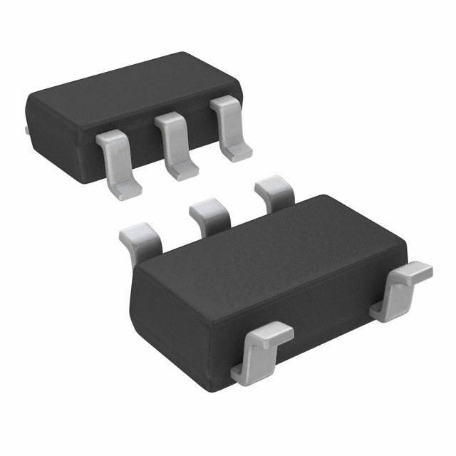
Space-Saving SOT23 and SC70 Packages
Ordering Information
Part Number
Top Mark
Eco Status
Package
Packing Method
NC7SZ38M5X
7Z38
RoHS
5-Lead SOT23, JEDEC MO-178 1.6mm
3000 Units on
Tape & Reel
NC7SZ38P5X
Z38
RoHS
5-Lead SC70, EIAJ SC-88a, 1.25mm Wide
3000 Units on
Tape & Reel
NC7SZ38L6X
A6
RoHS
6-Lead MicroPak™, 1.00mm Wide
5000 Units on
Tape & Reel
NC7SZ38FHX
A6
Green
6-Lead, MicroPak2, 1x1mm Body, .35mm
Pitch
5000 Units on
Tape & Reel
For Fairchild’s definition of Eco Status, please visit: http://www.fairchildsemi.com/company/green/rohs_green.html.
© 1996 Fairchild Semiconductor Corporation
NC7SZ38 • Rev. 1.0.3
www.fairchildsemi.com
NC7SZ38 — TinyLogic® UHS 2-Input NAND Gate, Open Drain Output
September 2009
�IEEE/IEC
Figure 1. Logic Symbol
Pin Configurations
Figure 2. SC70 and SOT23 (Top View)
Figure 3. MicroPak™ (Top Through View)
Pin Definitions
Pin # SC70 / SOT23
Pin # MicroPak
Name
1
1
A
Input
2
2
B
Input
3
3
GND
Ground
4
4
Y
Output
5
6
VCC
Supply Voltage
5
NC
No Connect
NC7SZ38 — UHS 2-Input NAND Gate, Open Drain Output
Connection Diagrams
Description
Function Table
Y= /AB
Inputs
Output
A
B
Y
L
L
*H
L
H
*H
H
L
*H
H
H
L
H = HIGH Logic Level
L = LOW Logic Level
*H = High Impedance Output State, Open Drain
© 1996 Fairchild Semiconductor Corporation
NC7SZ38 • Rev. 1.0.3
www.fairchildsemi.com
2
�Stresses exceeding the absolute maximum ratings may damage the device. The device may not function or be
operable above the recommended operating conditions and stressing the parts to these levels is not recommended.
In addition, extended exposure to stresses above the recommended operating conditions may affect device
reliability. The absolute maximum ratings are stress ratings only.
Symbol
VCC
VIN
VOUT
Parameter
Min.
Max.
Unit
Supply Voltage
-0.5
6.0
V
DC Input Voltage
-0.5
6.0
V
DC Output Voltage
-0.5
6.0
V
IIK
DC Input Diode Current
IOK
DC Output Diode Current
IOUT
DC Output Current
ICC or IGND
TSTG
VIN < -0.5V
-50
VIN > 6.0V
+20
VOUT < -0.5V
-50
VOUT > 6V, VCC=GND
+20
DC VCC or Ground Current
Storage Temperature Range
-65
TJ
Junction Temperature Under Bias
TL
Junction Lead Temperature (Soldering, 10 Seconds)
PD
ESD
Power Dissipation at +85°C
mA
mA
+50
mA
±50
mA
+150
°C
+150
°C
+260
°C
SOT-23
200
SC70-5
150
MicroPak-6
130
MicroPak2-6
120
Human Body Model, JEDEC:JESD22-A114
4000
Charge Device Model, JEDEC:JESD22-C101
2000
mW
NC7SZ38 — UHS 2-Input NAND Gate, Open Drain Output
Absolute Maximum Ratings
V
Recommended Operating Conditions
The Recommended Operating Conditions table defines the conditions for actual device operation. Recommended
operating conditions are specified to ensure optimal performance to the datasheet specifications. Fairchild does not
recommend exceeding them or designing to Absolute Maximum Ratings.
Symbol
VCC
VIN
VOUT
TA
Parameter
Conditions
Min.
Max.
Supply Voltage Operating
1.65
5.50
Supply Voltage Data Retention
1.50
5.50
Input Voltage
0
5.5
V
Output Voltage
0
5.5
V
-40
+85
°C
0
20
VCC=3.3V ± 0.3V
0
10
VCC=5.0V ± 0.5V
0
5
Operating Temperature
VCC=1.8V, 2.5V ± 0.2V
tr , tf
Input Rise and Fall Times
SOT-23
θJA
Thermal Resistance
Unit
V
ns/V
300
SC70-5
425
MicroPak-6
500
MicroPak2-6
560
°C/W
Note:
1. Unused inputs must be held HIGH or LOW. They may not float.
© 1996 Fairchild Semiconductor Corporation
NC7SZ38 • Rev. 1.0.3
www.fairchildsemi.com
3
�Symbol
Parameter
VIH
HIGH Level Input
Voltage
VIL
LOW Level Input
Voltage
ILKG
HIGH Level
Output Leakage
VCC
IIN
Min.
Typ.
TA=-40 to +85°C
Max.
Min.
1.65 to 1.95
0.75VCC
0.75VCC
2.30 to 5.50
0.70VCC
0.70VCC
V
0.25VCC
0.25VCC
2.30 to 5.50
0.30VCC
0.30VCC
±5
±10
5.50
LOW Level
Output Voltage
Input Leakage
Current
1.65
0.00
0.10
0.10
1.80
0.00
0.10
0.10
VIN=VIH, IOL=100
0.00
0.10
0.10
3.00
0.00
0.10
0.10
4.50
0.00
0.10
0.10
1.65
0.80
0.24
0.24
V
µA
V
2.30
IOL=8mA
0.10
0.30
0.30
3.00
IOL=16mA
0.15
0.40
0.40
3.00
IOL=24mA
0.22
0.55
0.55
4.50
IOL=32mA
0.22
0.55
0.55
5.50
VIN=5.5V, GND
±1
±10
µA
VIN or VOUT=5.5V
1
10
µA
VIN=5.5V, GND
2
20
µA
IOFF
Power Off
Leakage Current
0
ICC
Quiescent Supply
Current
5.50
© 1996 Fairchild Semiconductor Corporation
NC7SZ38 • Rev. 1.0.3
VIN=VIL,
VOUT=VCC or GND
Units
Max.
1.65 to 1.95
2.30
VOL
TA=+25°C
Conditions
NC7SZ38 — UHS 2-Input NAND Gate, Open Drain Output
DC Electrical Characteristics
www.fairchildsemi.com
4
�Symbol
Parameter
VCC
TA=+25°C
Conditions
Propagation Delay
tPLZ
CIN
Min.
Typ.
Max.
Min.
Max.
1.5
6.5
12.7
1.5
13.2
CL=50pF,
1.80
RU=500Ω,
2.50 ± 0.20
RD-500Ω,
3.30 ± 0.30 VIN=2•VCC
1.5
5.4
10.5
1.5
11.0
0.8
3.5
7.0
0.8
7.5
0.8
2.8
5.0
0.8
5.2
5.00 ± 0.50
0.5
2.2
4.3
0.5
4.5
1.65
1.5
5.5
12.7
1.5
13.2
1.80
CL=50pF,
RU=500Ω,
RD-500Ω,
3.30 ± 0.30 VIN=2•VCC
1.5
4.6
10.5
1.5
11.0
2.50 ± 0.20
0.8
3.0
7.0
0.8
7.5
0.8
2.1
6.0
0.8
5.2
5.00 ± 0.50
0.5
1.3
4.3
0.5
4.5
1.65
tPZL
TA=-40 to +85°C
Units
Figure
ns
Figure 4
Figure 5
Input Capacitance
0.00
4.0
pF
COUT
Output Capacitance
0.00
5.0
pF
CPD
Power Dissipation
Capacitance(2)
3.30
5.1
5.00
7.3
pF
Figure 6
Note:
2. CPD is defined as the value of the internal equivalent capacitance which is derived from dynamic operating
current consumption (ICCD) at no output loading and operating at 50% duty cycle. CPD is related to ICCD dynamic
operating current by the expression: ICCD=(CPD)(VCC)(fIN)+(ICCstatic).
NC7SZ38 — UHS 2-Input NAND Gate, Open Drain Output
AC Electrical Characteristics
Note:
3. CL includes load and stray capacitance.
Input PRR=10MHz tw=500ns.
Figure 4. AC Test Circuit
Figure 5. AC Waveforms
Note:
4. Input=AC Waveform; tr=tf=1.8ns; PRR=10MHz; Duty Cycle=50%.
Figure 6. Test Circuit
© 1996 Fairchild Semiconductor Corporation
NC7SZ38 • Rev. 1.0.3
www.fairchildsemi.com
5
�NC7SZ38 — UHS 2-Input NAND Gate, Open Drain Output
Physical Dimensions
3.00
2.80
5
SYMM
CL
0.95
0.95
A
4
B
3.00
2.60
1.70
1.50
1
2
2.60
3
(0.30)
1.00
0.50
0.30
0.95
0.20
1.90
C A B
0.70
TOP VIEW
LAND PATTERN RECOMMENDATION
SEE DETAIL A
1.30
0.90
1.45 MAX
0.15
0.05
0.22
0.08
C
0.10 C
NOTES: UNLESS OTHEWISE SPECIFIED
GAGE PLANE
A) THIS PACKAGE CONFORMS TO JEDEC
MO-178, ISSUE B, VARIATION AA,
B) ALL DIMENSIONS ARE IN MILLIMETERS.
C) MA05Brev5
0.25
8°
0°
0.55
0.35
0.60 REF
SEATING PLANE
Figure 7. 5-Lead SOT23, JEDEC MO-178 1.6mm
Package drawings are provided as a service to customers considering Fairchild components. Drawings may change in any manner
without notice. Please note the revision and/or date on the drawing and contact a Fairchild Semiconductor representative to verify
or obtain the most recent revision. Package specifications do not expand the terms of Fairchild’s worldwide terms and conditions, specifically
the warranty therein, which covers Fairchild products.
Always visit Fairchild Semiconductor’s online packaging area for the most recent package drawings:
http://www.fairchildsemi.com/packaging/.
Tape and Reel Specifications
Please visit Fairchild Semiconductor’s online packaging area for the most recent tape and reel specifications:
http://www.fairchildsemi.com/packaging/SOT23-5L_tr.pdf.
Package Designator
M5X
© 1996 Fairchild Semiconductor Corporation
NC7SZ38 • Rev. 1.0.3
Tape Section
Cavity Number
Cavity Status
Cover Type Status
Leader (Start End)
125 (Typical)
Empty
Sealed
Carrier
3000
Filled
Sealed
Trailer (Hub End)
75 (Typical)
Empty
Sealed
www.fairchildsemi.com
6
�NC7SZ38 — UHS 2-Input NAND Gate, Open Drain Output
Physical Dimensions
Figure 8. 5-Lead, SC70, EIAJ SC-88a, 1.25mm Wide
Package drawings are provided as a service to customers considering Fairchild components. Drawings may change in any manner
without notice. Please note the revision and/or date on the drawing and contact a Fairchild Semiconductor representative to verify
or obtain the most recent revision. Package specifications do not expand the terms of Fairchild’s worldwide terms and conditions, specifically
the warranty therein, which covers Fairchild products.
Always visit Fairchild Semiconductor’s online packaging area for the most recent package drawings:
http://www.fairchildsemi.com/packaging/.
Tape and Reel Specifications
Please visit Fairchild Semiconductor’s online packaging area for the most recent tape and reel specifications:
http://www.fairchildsemi.com/products/analog/pdf/sc70-5_tr.pdf.
Package Designator
P5X
© 1996 Fairchild Semiconductor Corporation
NC7SZ38 • Rev. 1.0.3
Tape Section
Cavity Number
Cavity Status
Cover Type Status
Leader (Start End)
125 (Typical)
Empty
Sealed
Carrier
3000
Filled
Sealed
Trailer (Hub End)
75 (Typical)
Empty
Sealed
www.fairchildsemi.com
7
�NC7SZ38 — UHS 2-Input NAND Gate, Open Drain Output
Physical Dimensions
2X
0.05 C
1.45
B
2X
(1)
0.05 C
(0.49)
5X
1.00
(0.75)
(0.52)
1X
A
TOP VIEW
0.55MAX
(0.30)
6X
PIN 1
0.05 C
0.05
0.00
RECOMMENED
LAND PATTERN
0.05 C
C
1.0
DETAIL A
0.10
0.05
0.45
0.35
0.10
0.00 6X
0.25
0.15 6X
C B A
C
0.40
0.30
0.35 5X
0.25
0.40 5X
0.30
0.5
(0.05)
6X
BOTTOM VIEW
DETAIL A
PIN 1 TERMINAL
0.075 X 45
CHAMFER
(0.13)
4X
Notes:
1. CONFORMS TO JEDEC STANDARD M0-252 VARIATION UAAD
2. DIMENSIONS ARE IN MILLIMETERS
3. DRAWING CONFORMS TO ASME Y14.5M-1994
MAC06AREVC
Figure 9. 6-Lead, MicroPak™, 1.0mm Wide
Package drawings are provided as a service to customers considering Fairchild components. Drawings may change in any manner
without notice. Please note the revision and/or date on the drawing and contact a Fairchild Semiconductor representative to verify
or obtain the most recent revision. Package specifications do not expand the terms of Fairchild’s worldwide terms and conditions, specifically
the warranty therein, which covers Fairchild products.
Always visit Fairchild Semiconductor’s online packaging area for the most recent package drawings:
http://www.fairchildsemi.com/packaging/.
Tape and Reel Specifications
Please visit Fairchild Semiconductor’s online packaging area for the most recent tape and reel specifications:
http://www.fairchildsemi.com/products/logic/pdf/micropak_tr.pdf.
Package Designator
L6X
© 1996 Fairchild Semiconductor Corporation
NC7SZ38 • Rev. 1.0.3
Tape Section
Cavity Number
Cavity Status
Cover Type Status
Leader (Start End)
125 (Typical)
Empty
Sealed
Carrier
5000
Filled
Sealed
Trailer (Hub End)
75 (Typical)
Empty
Sealed
www.fairchildsemi.com
8
�NC7SZ38 — UHS 2-Input NAND Gate, Open Drain Output
Physical Dimensions
DETAIL A
5X
Figure 10. 6-Lead, MicroPak2, 1x1mm Body, .35mm Pitch
Package drawings are provided as a service to customers considering Fairchild components. Drawings may change in any manner
without notice. Please note the revision and/or date on the drawing and contact a Fairchild Semiconductor representative to verify
or obtain the most recent revision. Package specifications do not expand the terms of Fairchild’s worldwide terms and conditions, specifically
the warranty therein, which covers Fairchild products.
Always visit Fairchild Semiconductor’s online packaging area for the most recent package drawings:
http://www.fairchildsemi.com/packaging/.
Tape and Reel Specifications
Please visit Fairchild Semiconductor’s online packaging area for the most recent tape and reel specifications:
http://www.fairchildsemi.com/packaging/MicroPAK2_6L_tr.pdf.
Package Designator
FHX
© 1996 Fairchild Semiconductor Corporation
NC7SZ38 • Rev. 1.0.3
Tape Section
Cavity Number
Cavity Status
Cover Type Status
Leader (Start End)
125 (Typical)
Empty
Sealed
Carrier
5000
Filled
Sealed
Trailer (Hub End)
75 (Typical)
Empty
Sealed
www.fairchildsemi.com
9
�NC7SZ38 — UHS 2-Input NAND Gate, Open Drain Output
© 1996 Fairchild Semiconductor Corporation
NC7SZ38 • Rev. 1.0.3
www.fairchildsemi.com
10
�ON Semiconductor and
are trademarks of Semiconductor Components Industries, LLC dba ON Semiconductor or its subsidiaries in the United States and/or other countries.
ON Semiconductor owns the rights to a number of patents, trademarks, copyrights, trade secrets, and other intellectual property. A listing of ON Semiconductor’s product/patent
coverage may be accessed at www.onsemi.com/site/pdf/Patent−Marking.pdf. ON Semiconductor reserves the right to make changes without further notice to any products herein.
ON Semiconductor makes no warranty, representation or guarantee regarding the suitability of its products for any particular purpose, nor does ON Semiconductor assume any liability
arising out of the application or use of any product or circuit, and specifically disclaims any and all liability, including without limitation special, consequential or incidental damages.
Buyer is responsible for its products and applications using ON Semiconductor products, including compliance with all laws, regulations and safety requirements or standards,
regardless of any support or applications information provided by ON Semiconductor. “Typical” parameters which may be provided in ON Semiconductor data sheets and/or
specifications can and do vary in different applications and actual performance may vary over time. All operating parameters, including “Typicals” must be validated for each customer
application by customer’s technical experts. ON Semiconductor does not convey any license under its patent rights nor the rights of others. ON Semiconductor products are not
designed, intended, or authorized for use as a critical component in life support systems or any FDA Class 3 medical devices or medical devices with a same or similar classification
in a foreign jurisdiction or any devices intended for implantation in the human body. Should Buyer purchase or use ON Semiconductor products for any such unintended or unauthorized
application, Buyer shall indemnify and hold ON Semiconductor and its officers, employees, subsidiaries, affiliates, and distributors harmless against all claims, costs, damages, and
expenses, and reasonable attorney fees arising out of, directly or indirectly, any claim of personal injury or death associated with such unintended or unauthorized use, even if such
claim alleges that ON Semiconductor was negligent regarding the design or manufacture of the part. ON Semiconductor is an Equal Opportunity/Affirmative Action Employer. This
literature is subject to all applicable copyright laws and is not for resale in any manner.
PUBLICATION ORDERING INFORMATION
LITERATURE FULFILLMENT:
Literature Distribution Center for ON Semiconductor
19521 E. 32nd Pkwy, Aurora, Colorado 80011 USA
Phone: 303−675−2175 or 800−344−3860 Toll Free USA/Canada
Fax: 303−675−2176 or 800−344−3867 Toll Free USA/Canada
Email: orderlit@onsemi.com
© Semiconductor Components Industries, LLC
N. American Technical Support: 800−282−9855 Toll Free
USA/Canada
Europe, Middle East and Africa Technical Support:
Phone: 421 33 790 2910
Japan Customer Focus Center
Phone: 81−3−5817−1050
www.onsemi.com
1
ON Semiconductor Website: www.onsemi.com
Order Literature: http://www.onsemi.com/orderlit
For additional information, please contact your local
Sales Representative
www.onsemi.com
�


 工商网监
湘ICP备2023018690号
工商网监
湘ICP备2023018690号