DATA SHEET
www.onsemi.com
TinyLogic ULP-A Dual
Inverter with
Schmitt-Trigger Input
MARKING
DIAGRAMS
SIP6 1.45X1.0
MicroPak
CASE 127EB
NC7WV14
CCKK
XYZ
Pin 1
The NC7WV14 is a dual inverter with Schmitt−trigger input in tiny
footprint packages. The device is designed to operate for VCC = 0.9 V
to 3.6 V.
CC
KK
XY
Z
= Specific Device Code
= 2−Digit Lot Run Traceability Code
= 2−Digit Date Code
= Assembly Plant Code
Features
•
•
•
•
•
•
•
Designed for 0.9 V to 3.6 V VCC Operation
2.2 ns tPD at 3.3 V (Typ)
Inputs/Outputs Over−Voltage Tolerant up to 3.6 V
IOFF Supports Partial Power Down Protection
Source/Sink 24 mA at 3.3 V
Available in SC−88 and MicroPak™ Packages
These Devices are Pb−Free, Halogen Free/BFR Free and are RoHS
Compliant
6
SC−88
DF SUFFIX
CASE 419AD
XXXMG
G
1
1
XXX = Specific Devic Code
M
= Date Code
G
= Pb−Free Package
(Note: Microdot may be in either location)
A1 1
6
Y1
GND 2
5
VCC
A2 3
4
Y2
A1 1
GND
6 Y1
2
*Date Code orientation and/or position may vary
depending upon manufacturing location.
5 VCC
A2 3
4 Y2
MicroPak
SC−88
ORDERING INFORMATION
See detailed ordering, marking and shipping information on
page 7 of this data sheet.
Figure 1. Pinout Diagrams (Top Views)
A1
A2
1
Y1
1
Y2
Figure 2. Logic Symbol
PIN ASSIGNMENT
FUNCTION TABLE
Pin
Function
Input
Output
1
A1
L
H
2
GND
H
L
3
A2
4
Y2
5
VCC
6
Y1
© Semiconductor Components Industries, LLC, 2003
July, 2022 − Rev. 3
1
Publication Order Number:
NC7WV14/D
�NC7WV14
MAXIMUM RATINGS
Symbol
Value
Unit
VCC
DC Supply Voltage
−0.5 to +4.3
V
VIN
DC Input Voltage
−0.5 to +4.3
V
−0.5 to VCC + 0.5
−0.5 to +4.3
−0.5 to +4.3
V
VIN < GND
−50
mA
VOUT < GND
−50
mA
VOUT
Characteristics
DC Output Voltage
Active−Mode (High or Low State)
Tri−State Mode (Note 1)
Power−Down Mode (VCC = 0 V)
IIK
DC Input Diode Current
IOK
DC Output Diode Current
IOUT
DC Output Source/Sink Current
±50
mA
DC Supply Current per Supply Pin or Ground Pin
±50
mA
ICC or IGND
TSTG
−65 to +150
°C
TL
Storage Temperature Range
Lead Temperature, 1 mm from Case for 10 Seconds
260
°C
TJ
Junction Temperature Under Bias
+150
°C
qJA
Thermal Resistance (Note 2)
SC−88
MicroPak
377
154
°C/W
PD
Power Dissipation in Still Air
SC−88
MicroPak
332
812
mW
Level 1
−
Oxygen Index: 28 to 34
UL 94 V−0 @ 0.125 in
−
Human Body Mode
Charged Device Mode
2000
1000
V
±100
mA
MSL
Moisture Sensitivity
FR
Flammability Rating
VESD
ILatchup
ESD Withstand Voltage (Note 3)
Latchup Performance (Note 4)
Stresses exceeding those listed in the Maximum Ratings table may damage the device. If any of these limits are exceeded, device functionality
should not be assumed, damage may occur and reliability may be affected.
1. Applicable to devices with outputs that may be tri−stated.
2. Measured with minimum pad spacing on an FR4 board, using 10 mm−by−1 inch, 2 ounce copper trace no air flow per JESD51−7.
3. HBM tested to EIA / JESD22−A114−A. CDM tested to JESD22−C101−A. JEDEC recommends that ESD qualification to EIA/JESD22−A115A
(Machine Model) be discontinued.
4. Tested to EIA/JESD78 Class II.
www.onsemi.com
2
�NC7WV14
RECOMMENDED OPERATING CONDITIONS
Symbol
Parameter
VCC
Positive DC Supply Voltage
VIN
DC Input Voltage
VOUT
TA
tr , tf
DC Output Voltage
Active−Mode (High or Low State)
Tri−State Mode (Note 1)
Power−Down Mode (VCC = 0 V)
Operating Temperature Range
Input Transition Rise and Fall Time
Min
Max
Unit
0.9
3.6
V
0
3.6
V
0
0
0
VCC
3.6
3.6
−40
+85
°C
0
No Limit
ns/V
Functional operation above the stresses listed in the Recommended Operating Ranges is not implied. Extended exposure to stresses beyond
the Recommended Operating Ranges limits may affect device reliability.
DC ELECTRICAL CHARACTERISTICS
TA = 255C
Symbol
Parameter
VP
Positive
Threshold Voltage
VN
VH
Negative
Threshold Voltage
Hysteresis
Voltage
Condition
VCC (V)
Min
Typ
0.9
−
1.1
−
1.4
TA = −405C to +855C
Max
Min
Max
Unit
0.62
−
−
1.0
−
−
V
−
1.0
−
−
1.25
−
1.25
1.65
−
2.3
−
−
1.5
−
1.5
−
1.8
−
1.8
2.7
0.9
−
−
2.2
−
2.2
−
0.34
−
−
−
1.1
0.15
−
−
0.15
−
1.4
0.2
−
−
0.2
−
1.65
0.25
−
−
0.25
−
2.3
0.4
−
−
0.4
−
2.7
0.6
−
−
0.6
−
0.9
−
0.29
−
−
−
1.1
0.08
−
0.6
0.08
0.6
1.4
0.09
−
0.8
0.09
0.8
1.65
0.15
−
1.0
0.15
1.0
2.3
0.25
−
1.1
0.25
1.1
2.7
0.6
−
1.2
0.6
1.2
www.onsemi.com
3
V
V
�NC7WV14
DC ELECTRICAL CHARACTERISTICS (continued)
TA = −405C to +855C
TA = 255C
Symbol
Parameter
VOH
High−Level Output
Voltage
Condition
Low−Level
Output Voltage
Input Leakage
Current
Max
Min
Max
−
VCC – 0.1
−
−
−
1.1 to 1.3
VCC – 0.1
−
−
VCC – 0.1
−
1.4 to 1.6
VCC – 0.1
−
−
VCC – 0.1
−
1.65 to 1.95
VCC – 0.2
−
−
VCC – 0.2
−
2.3 to
很抱歉,暂时无法提供与“NC7WV14L6X”相匹配的价格&库存,您可以联系我们找货
免费人工找货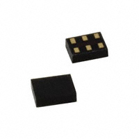


 工商网监
湘ICP备2023018690号
工商网监
湘ICP备2023018690号
