Is Now Part of
To learn more about ON Semiconductor, please visit our website at
www.onsemi.com
Please note: As part of the Fairchild Semiconductor integration, some of the Fairchild orderable part numbers
will need to change in order to meet ON Semiconductor’s system requirements. Since the ON Semiconductor
product management systems do not have the ability to manage part nomenclature that utilizes an underscore
(_), the underscore (_) in the Fairchild part numbers will be changed to a dash (-). This document may contain
device numbers with an underscore (_). Please check the ON Semiconductor website to verify the updated
device numbers. The most current and up-to-date ordering information can be found at www.onsemi.com. Please
email any questions regarding the system integration to Fairchild_questions@onsemi.com.
ON Semiconductor and the ON Semiconductor logo are trademarks of Semiconductor Components Industries, LLC dba ON Semiconductor or its subsidiaries in the United States and/or other countries. ON Semiconductor owns the rights to a number
of patents, trademarks, copyrights, trade secrets, and other intellectual property. A listing of ON Semiconductor’s product/patent coverage may be accessed at www.onsemi.com/site/pdf/Patent-Marking.pdf. ON Semiconductor reserves the right
to make changes without further notice to any products herein. ON Semiconductor makes no warranty, representation or guarantee regarding the suitability of its products for any particular purpose, nor does ON Semiconductor assume any liability
arising out of the application or use of any product or circuit, and specifically disclaims any and all liability, including without limitation special, consequential or incidental damages. Buyer is responsible for its products and applications using ON
Semiconductor products, including compliance with all laws, regulations and safety requirements or standards, regardless of any support or applications information provided by ON Semiconductor. “Typical” parameters which may be provided in ON
Semiconductor data sheets and/or specifications can and do vary in different applications and actual performance may vary over time. All operating parameters, including “Typicals” must be validated for each customer application by customer’s
technical experts. ON Semiconductor does not convey any license under its patent rights nor the rights of others. ON Semiconductor products are not designed, intended, or authorized for use as a critical component in life support systems or any FDA
Class 3 medical devices or medical devices with a same or similar classification in a foreign jurisdiction or any devices intended for implantation in the human body. Should Buyer purchase or use ON Semiconductor products for any such unintended
or unauthorized application, Buyer shall indemnify and hold ON Semiconductor and its officers, employees, subsidiaries, affiliates, and distributors harmless against all claims, costs, damages, and expenses, and reasonable attorney fees arising out
of, directly or indirectly, any claim of personal injury or death associated with such unintended or unauthorized use, even if such claim alleges that ON Semiconductor was negligent regarding the design or manufacture of the part. ON Semiconductor
is an Equal Opportunity/Affirmative Action Employer. This literature is subject to all applicable copyright laws and is not for resale in any manner.
�NC7WZ132
TinyLogic® UHS Dual 2-Input NAND Gate with Schmitt
Trigger Inputs
Features
General Description
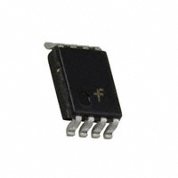
■ Space saving US8 surface mount package
The NC7WZ132 is a dual 2-Input NAND Gate from
Fairchild's Ultra High Speed Series of TinyLogic®. The
device is fabricated with advanced CMOS technology to
achieve ultra high speed with high output drive while
maintaining low static power dissipation over a broad
VCC operating range. The device is specified to operate
over the 1.65V to 5.5V VCC operating range. The inputs
and output are high impedance when VCC is 0V. Inputs
tolerate voltages up to 7V independent of VCC operating
voltage. Schmitt trigger inputs achieve typically 1V hysteresis between the positive-going and negative-going
input threshold voltage at 5V VCC.
■ MicroPak™ leadless package
■ Ultra High Speed; tPD 3.1ns typ. into 50pF at 5V VCC
■ High Output Drive; ±24mA at 3V VCC
■ Broad VCC Operating Range; 1.65V to 5.5V
■ Matches the performance of LCX when operated at
3.3V VCC
■ Power down high impedance inputs/output
■ Overvoltage tolerant inputs facilitate 5V to 3V
translation
■ Proprietary noise/EMI reduction circuitry implemented
■ Schmitt trigger inputs are tolerant of slow changing
input signals
Ordering Information
Order
Number
Package
Number
Product Code
Top Mark
NC7WZ132K8X
MAB08A
WZD2
8-Lead US8, JEDEC MO-187,
Variation CA 3.1mm Wide
3k Units on Tape and
Reel
NC7WZ132L8X
MAC08A
T5
8-Lead MicroPak, 1.6 mm Wide
5k Units on Tape and
Reel
Package Description
Supplied As
Device also available in Tape and Reel. Specify by appending suffix letter “X” to the ordering number.
All packages are lead free per JEDEC: J-STD-020B standard.
©2000 Fairchild Semiconductor Corporation
NC7WZ132 Rev. 1.11.0
www.fairchildsemi.com
NC7WZ132 — TinyLogic® UHS Dual 2-Input NAND Gate with Schmitt Trigger Inputs
March 2008
�IEEE/IEC
Function Table
(Top View)
Y = AB
Pin One Orientation Diagram
(Top View)
Inputs
AAA
Pin One
AAA represents Product Code Top Mark – see ordering
code
Output
A
B
Y
L
L
H
L
H
H
H
L
H
H
H
L
H = HIGH Logic Level
L = LOW Logic Level
Note: Orientation of Top Mark determines Pin One
location. Read the top product code mark left to right,
Pin One is the lower left pin (see diagram).
Pad Assignments for MicroPak
(Top Thru View)
Pin Description
Pin Names
Description
An, Bn
Inputs
Yn
Output
©2000 Fairchild Semiconductor Corporation
NC7WZ132 Rev. 1.11.0
www.fairchildsemi.com
2
NC7WZ132 — TinyLogic® UHS Dual 2-Input NAND Gate with Schmitt Trigger Inputs
Logic Symbol
Connection Diagram
�Stresses exceeding the absolute maximum ratings may damage the device. The device may not function or be
operable above the recommended operating conditions and stressing the parts to these levels is not recommended.
In addition, extended exposure to stresses above the recommended operating conditions may affect device reliability.
The absolute maximum ratings are stress ratings only.
Symbol
Parameter
Rating
VCC
Supply Voltage
–0.5V to +7V
VIN
DC Input Voltage
–0.5V to +7V
DC Output Voltage
–0.5V to +7V
VOUT
IIK
DC Input Diode Current @ VIN < –0.5V
–50mA
IOK
DC Output Diode Current @ VOUT < –0.5V
–50mA
IOUT
DC Output Current
±50mA
ICC / IGND
DC VCC / GND Current
TSTG
Storage Temperature
±100mA
–65°C to +150°C
TJ
Junction Temperature Under Bias
150°C
TL
Junction Lead Temperature (Soldering, 10 seconds)
260°C
PD
Power Dissipation @ +85°C
250mW
Recommended Operating Conditions(1)
The Recommended Operating Conditions table defines the conditions for actual device operation. Recommended
operating conditions are specified to ensure optimal performance to the datasheet specifications. Fairchild does not
recommend exceeding them or designing to absolute maximum ratings.
Symbol
VCC
Parameter
Supply Voltage Operating
1.65V to 5.5V
Supply Voltage Data Retention
VIN
VOUT
Rating
1.5V to 5.5V
Input Voltage
0V to 5.5V
Output Voltage
0V to VCC
TA
Operating Temperature
θJA
Thermal Resistance
–40°C to +85°C
250°C/W
Note:
1. Unused inputs must be held HIGH or LOW. They may not float.
©2000 Fairchild Semiconductor Corporation
NC7WZ132 Rev. 1.11.0
www.fairchildsemi.com
3
NC7WZ132 — TinyLogic® UHS Dual 2-Input NAND Gate with Schmitt Trigger Inputs
Absolute Maximum Ratings
�TA = –40°C
to +85°C
TA = +25°C
Symbol
Parameter
VCC (V)
VP
Positive Threshold
Voltage
1.65
0.6
0.99
1.4
0.6
1.4
2.3
1.0
1.39
1.8
1.0
1.8
3.0
1.3
1.77
2.2
1.3
2.2
4.5
1.9
2.49
3.1
1.9
3.1
5.5
2.2
2.96
3.6
2.2
3.6
1.65
0.2
0.53
0.9
0.2
0.9
2.3
0.4
0.78
1.15
0.4
1.15
3.0
0.6
1.02
1.5
0.6
1.5
4.5
1.0
1.48
2.0
1.0
2.0
VN
VH
Negative Threshold
Voltage
Hysteresis Voltage
Conditions
HIGH Level Output
Voltage
IIN
LOW Level Output
Voltage
Input Leakage
Current
IOFF
Power Off
Leakage Current
ICC
Quiescent Supply
Current
©2000 Fairchild Semiconductor Corporation
NC7WZ132 Rev. 1.11.0
Min.
Max. Units
5.5
1.2
1.76
2.3
1.2
2.3
0.15
0.46
0.9
0.15
0.9
2.3
0.25
0.61
1.1
0.25
1.1
3.0
0.4
0.75
1.2
0.4
1.2
4.5
0.6
1.01
1.5
0.6
1.5
1.7
0.7
1.7
0.7
1.20
1.55
1.65
1.55
2.3
2.2
2.3
2.2
3.0
2.9
3.0
2.9
1.65
VIN = VIL
IOH = –100µA
4.5
VOL
Typ. Max.
1.65
5.5
VOH
Min.
4.4
4.5
4.4
1.65
IOH = –4mA
1.29
1.52
1.29
2.3
IOH = –8mA
1.9
2.15
1.9
3.0
IOH = –16mA
2.4
2.80
2.4
3.0
IOH = –24mA
2.3
2.68
2.3
4.5
IOH = –32mA
3.8
4.20
3.8
1.65
VIN = VIH IOL = 100µA
V
V
V
V
0.0
0.10
0.10
2.3
0.0
0.10
0.10
3.0
0.0
0.10
0.10
4.5
0.0
0.10
0.10
V
1.65
IOL = 4mA
0.08
0.24
0.24
2.3
IOL = 8mA
0.10
0.3
0.3
3.0
IOL = 16mA
0.15
0.4
0.4
3.0
IOL = 24mA
0.22
0.55
0.55
4.5
IOL = 32mA
0.22
0.55
0.55
±0.1
±1
µA
1
10
µA
1
10
µA
0 to 5.5
0.0
VIN = 5.5V, GND
VIN or VOUT = 5.5V
1.65 to 5.5 VIN = 5.5V, GND
www.fairchildsemi.com
4
NC7WZ132 — TinyLogic® UHS Dual 2-Input NAND Gate with Schmitt Trigger Inputs
DC Electrical Characteristics
�TA = –40°C
to +85°C
TA = +25°C
Symbol
Parameter
tPLH, tPHL
Propagation Delay
tPLH, tPHL
Propagation Delay
CIN
Input Capacitance
VCC (V)
Power Dissipation
Capacitance
Typ.
Max.
Max.
Units
ns
Figure 1
Figure 3
ns
Figure 1
Figure 3
3.0
7.1
13.0
3.0
13.5
2.0
4.5
7.5
2.0
8.0
3.3 ± 0.3
1.2
3.4
5.0
1.2
5.5
5.0 ± 0.5
0.8
2.6
3.8
0.8
4.2
1.8
4.0
5.8
1.8
6.3
1.2
3.1
4.5
1.2
4.9
3.3 ± 0.3
CL = 50pF,
RL = 500Ω
0
3.3
(2)
5.0
Figure
Number
Min.
1.8 ± 0.15 CL = 15 pF,
2.5 ± 0.2 RL = 1MΩ
5.0 ± 0.5
CPD
Min.
Conditions
2.5
pF
15
pF
Figure 2
18
Note:
2. CPD is defined as the value of the internal equivalent capacitance which is derived from dynamic operating current
consumption (ICCD) at no output loading and operating at 50% duty cycle. (See Figure 2.) CPD is related to ICCD
dynamic operating current by the expression: ICCD = (CPD)(VCC)(fIN) +(ICCstatic).
AC Loading and Waveforms
CL includes load and stray capacitance
Input PRR = 1.0 MHz; tw = 500ns
Figure 1. AC Test Circuit
Figure 3. AC Waveforms
Input = AC Waveform; tr = tf = 1.8ns;
PRR = 10 MHz;Duty Cycle = 50%
Figure 2. ICCD Test Circuit
©2000 Fairchild Semiconductor Corporation
NC7WZ132 Rev. 1.11.0
www.fairchildsemi.com
5
NC7WZ132 — TinyLogic® UHS Dual 2-Input NAND Gate with Schmitt Trigger Inputs
AC Electrical Characteristics
�Tape Format for US8
Package Designator
Tape Section
Number of Cavities
Cavity Status
Cover Tape Status
K8X
Leader (Start End)
125 (typ.)
Empty
Sealed
Carrier
3000
Filled
Sealed
Trailer (Hub End)
75 (typ.)
Empty
Sealed
Tape Dimensions inches (millimeters)
Tape Format for MicroPak
Package Designator
Tape Section
Number of Cavities
Cavity Status
Cover Tape Status
L8X
Leader (Start End)
125 (typ.)
Empty
Sealed
Carrier
3000
Filled
Sealed
Trailer (Hub End)
75 (typ.)
Empty
Sealed
Tape Dimensions inches (millimeters)
©2000 Fairchild Semiconductor Corporation
NC7WZ132 Rev. 1.11.0
www.fairchildsemi.com
6
NC7WZ132 — TinyLogic® UHS Dual 2-Input NAND Gate with Schmitt Trigger Inputs
Tape and Reel Specifications
�Reel Dimensions inches (millimeters)
Tape
Size
8mm
A
B
7.0
(177.8)
0.059
(1.50)
©2000 Fairchild Semiconductor Corporation
NC7WZ132 Rev. 1.11.0
C
D
N
0.512
0.795
2.165
(13.00) (20.20) (55.00)
W1
W2
W3
0.331 +0.059/–0.000
(8.40 +1.50/–0.00)
0.567
(14.40)
W1 +0.078/–0.039
(W1 +2.00/–1.00)
www.fairchildsemi.com
7
NC7WZ132 — TinyLogic® UHS Dual 2-Input NAND Gate with Schmitt Trigger Inputs
Tape and Reel Specifications (Continued)
�8
5
0.70
-B-
2.3±0.1
3.1±.1
2.70
0.15
3.40
-A-
1.80
1.00
1.55
0.30 TYP
1
0.2 C B A
ALL LEAD TIPS
4
PIN #1 IDENT.
ALL LEAD TIPS
0.1 C
0.90 MAX
0.5 TYP
DETAIL A
0.70±0.10
0.10-0.18
-C0.10
0.00
0.17-0.27
0.13
0.50TYP
A B
C
0.4 TYP
GAGE PLANE
0.12
0°-8°
A. CONFORMS TO JEDEC REGISTRATION MO-187
B. DIMENSIONS ARE IN MILLIMETERS.
C. DIMENSIONS ARE EXCLUSIVE OF BURRS, MOLD FLASH,
AND TIE BAR EXTRUSIONS.
SEATING PLANE
DETAIL A
D. DIMENSIONS AND TOLERANCES PER ANSI Y14.5M, 1982.
MAB08AREVC
Figure 4. 8-Lead US8, JEDEC MO-187, Variation CA 3.1mm Wide
Package drawings are provided as a service to customers considering Fairchild components. Drawings may change in any manner
without notice. Please note the revision and/or date on the drawing and contact a Fairchild Semiconductor representative to verify or
obtain the most recent revision. Package specifications do not expand the terms of Fairchild’s worldwide terms and conditions,
specifically the warranty therein, which covers Fairchild products.
Always visit Fairchild Semiconductor’s online packaging area for the most recent package drawings:
http://www.fairchildsemi.com/packaging/
©2000 Fairchild Semiconductor Corporation
NC7WZ132 Rev. 1.11.0
www.fairchildsemi.com
8
NC7WZ132 — TinyLogic® UHS Dual 2-Input NAND Gate with Schmitt Trigger Inputs
Physical Dimensions
�NC7WZ132 — TinyLogic® UHS Dual 2-Input NAND Gate with Schmitt Trigger Inputs
Physical Dimensions (Continued)
Figure 5. 8-Lead MicroPak, 1.6 mm Wide
Package drawings are provided as a service to customers considering Fairchild components. Drawings may change in any manner
without notice. Please note the revision and/or date on the drawing and contact a Fairchild Semiconductor representative to verify or
obtain the most recent revision. Package specifications do not expand the terms of Fairchild’s worldwide terms and conditions,
specifically the warranty therein, which covers Fairchild products.
Always visit Fairchild Semiconductor’s online packaging area for the most recent package drawings:
http://www.fairchildsemi.com/packaging/
©2000 Fairchild Semiconductor Corporation
NC7WZ132 Rev. 1.11.0
www.fairchildsemi.com
9
�ACEx®
Build it Now™
CorePLUS™
CROSSVOLT™
CTL™
Current Transfer Logic™
EcoSPARK®
EZSWITCH™ *
™
PDP-SPM™
Power220®
POWEREDGE®
Power-SPM™
PowerTrench®
Programmable Active Droop™
QFET®
QS™
QT Optoelectronics™
Quiet Series™
RapidConfigure™
SMART START™
SPM®
STEALTH™
SuperFET™
SuperSOT™-3
SuperSOT™-6
SuperSOT™-8
FPS™
FRFET®
Global Power ResourceSM
Green FPS™
Green FPS™e-Series™
GTO™
i-Lo™
IntelliMAX™
ISOPLANAR™
MegaBuck™
MICROCOUPLER™
MicroFET™
MicroPak™
MillerDrive™
Motion-SPM™
OPTOLOGIC®
OPTOPLANAR®
®
Fairchild®
Fairchild Semiconductor®
FACT Quiet Series™
FACT®
FAST®
FastvCore™
FlashWriter® *
®
SupreMOS™
SyncFET™
®
The Power Franchise®
TinyBoost™
TinyBuck™
TinyLogic®
TINYOPTO™
TinyPower™
TinyPWM™
TinyWire™
µSerDes™
UHC®
Ultra FRFET™
UniFET™
VCX™
* EZSWITCH™ and FlashWriter® are trademarks of System General Corporation, used under license by Fairchild Semiconductor.
DISCLAIMER
FAIRCHILD SEMICONDUCTOR RESERVES THE RIGHT TO MAKE CHANGES WITHOUT FURTHER NOTICE TO ANY PRODUCTS
HEREIN TO IMPROVE RELIABILITY, FUNCTION, OR DESIGN. FAIRCHILD DOES NOT ASSUME ANY LIABILITY ARISING OUT OF THE
APPLICATION OR USE OF ANY PRODUCT OR CIRCUIT DESCRIBED HEREIN; NEITHER DOES IT CONVEY ANY LICENSE UNDER ITS
PATENT RIGHTS, NOR THE RIGHTS OF OTHERS. THESE SPECIFICATIONS DO NOT EXPAND THE TERMS OF FAIRCHILD’S
WORLDWIDE TERMS AND CONDITIONS, SPECIFICALLY THE WARRANTY THEREIN, WHICH COVERS THESE PRODUCTS.
LIFE SUPPORT POLICY
FAIRCHILD’S PRODUCTS ARE NOT AUTHORIZED FOR USE AS CRITICAL COMPONENTS IN LIFE SUPPORT DEVICES OR
SYSTEMS WITHOUT THE EXPRESS WRITTEN APPROVAL OF FAIRCHILD SEMICONDUCTOR CORPORATION.
As used herein:
1. Life support devices or systems are devices or systems
which, (a) are intended for surgical implant into the body or
(b) support or sustain life, and (c) whose failure to perform
when properly used in accordance with instructions for use
provided in the labeling, can be reasonably expected to
result in a significant injury of the user.
2. A critical component in any component of a life support,
device, or system whose failure to perform can be
reasonably expected to cause the failure of the life support
device or system, or to affect its safety or effectiveness.
PRODUCT STATUS DEFINITIONS
Definition of Terms
Datasheet Identification
Product Status
Definition
Advance Information
Formative or In Design
This datasheet contains the design specifications for product
development. Specifications may change in any manner without notice.
Preliminary
First Production
This datasheet contains preliminary data; supplementary data will be
published at a later date. Fairchild Semiconductor reserves the right to
make changes at any time without notice to improve design.
No Identification Needed
Full Production
This datasheet contains final specifications. Fairchild Semiconductor
reserves the right to make changes at any time without notice to improve
the design.
Obsolete
Not In Production
This datasheet contains specifications on a product that has been
discontinued by Fairchild Semiconductor. The datasheet is printed for
reference information only.
Rev. I33
©2000 Fairchild Semiconductor Corporation
NC7WZ132 Rev. 1.11.0
www.fairchildsemi.com
10
NC7WZ132 — TinyLogic® UHS Dual 2-Input NAND Gate with Schmitt Trigger Inputs
TRADEMARKS
The following includes registered and unregistered trademarks and service marks, owned by Fairchild Semiconductor and/or its global
subsidiaries, and is not intended to be an exhaustive list of all such trademarks.
�ON Semiconductor and
are trademarks of Semiconductor Components Industries, LLC dba ON Semiconductor or its subsidiaries in the United States and/or other countries.
ON Semiconductor owns the rights to a number of patents, trademarks, copyrights, trade secrets, and other intellectual property. A listing of ON Semiconductor’s product/patent
coverage may be accessed at www.onsemi.com/site/pdf/Patent−Marking.pdf. ON Semiconductor reserves the right to make changes without further notice to any products herein.
ON Semiconductor makes no warranty, representation or guarantee regarding the suitability of its products for any particular purpose, nor does ON Semiconductor assume any liability
arising out of the application or use of any product or circuit, and specifically disclaims any and all liability, including without limitation special, consequential or incidental damages.
Buyer is responsible for its products and applications using ON Semiconductor products, including compliance with all laws, regulations and safety requirements or standards,
regardless of any support or applications information provided by ON Semiconductor. “Typical” parameters which may be provided in ON Semiconductor data sheets and/or
specifications can and do vary in different applications and actual performance may vary over time. All operating parameters, including “Typicals” must be validated for each customer
application by customer’s technical experts. ON Semiconductor does not convey any license under its patent rights nor the rights of others. ON Semiconductor products are not
designed, intended, or authorized for use as a critical component in life support systems or any FDA Class 3 medical devices or medical devices with a same or similar classification
in a foreign jurisdiction or any devices intended for implantation in the human body. Should Buyer purchase or use ON Semiconductor products for any such unintended or unauthorized
application, Buyer shall indemnify and hold ON Semiconductor and its officers, employees, subsidiaries, affiliates, and distributors harmless against all claims, costs, damages, and
expenses, and reasonable attorney fees arising out of, directly or indirectly, any claim of personal injury or death associated with such unintended or unauthorized use, even if such
claim alleges that ON Semiconductor was negligent regarding the design or manufacture of the part. ON Semiconductor is an Equal Opportunity/Affirmative Action Employer. This
literature is subject to all applicable copyright laws and is not for resale in any manner.
PUBLICATION ORDERING INFORMATION
LITERATURE FULFILLMENT:
Literature Distribution Center for ON Semiconductor
19521 E. 32nd Pkwy, Aurora, Colorado 80011 USA
Phone: 303−675−2175 or 800−344−3860 Toll Free USA/Canada
Fax: 303−675−2176 or 800−344−3867 Toll Free USA/Canada
Email: orderlit@onsemi.com
© Semiconductor Components Industries, LLC
N. American Technical Support: 800−282−9855 Toll Free
USA/Canada
Europe, Middle East and Africa Technical Support:
Phone: 421 33 790 2910
Japan Customer Focus Center
Phone: 81−3−5817−1050
www.onsemi.com
1
ON Semiconductor Website: www.onsemi.com
Order Literature: http://www.onsemi.com/orderlit
For additional information, please contact your local
Sales Representative
www.onsemi.com
�