Test Procedure for the NCP1207AADAPGEVB
01/31/2005
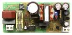
1.0 Diagrams
1.1 Test Configuration
Figure 1. NCP1207AADAPGEVB Test Configuration.
�1.2 Oscilloscope Test Points
Figure 2. NCP1207AADAPGEVB Oscilloscope Test Points.
2.0 Equipment
•
•
•
•
•
•
Variable AC Power supply (0 ~ 240 VAC, 1.0 A)
Ammeter (0 ~ 1.0 A)
Ammeter (0 ~ 3.0 A)
Voltmeter (0 ~ 20 VDC)
Electronic Load (capable of sinking 3.0 A @ 12 VDC)
Oscilloscope (100 MHz, 120 V, 2-Channel)
�3.0 Test Procedure
3.1 Set load to 0.0 A. Apply 180 VAC supply. Verify that output voltage is 12.0 V ±1%.
Input current should not exceed 20 mA.
3.2 Increase load current to 0.1 A. Gate driver and drain voltage should be as in Figure 3.
Verify that output voltage is 12.0 V ±1%. Input current should not exceed 200 mA.
Figure 3. Gate Driver and Drain Voltage at Very Light Load
�3.3 Increase load current to 2.0 A. Gate driver and drain voltage should be as in Figure 4.
Verify that output voltage is 12.0 V ±1%. Input current should not exceed 200 mA.
Figure 4. Gate Driver and Drain Voltage at Full Load.
3.4 Increase supply voltage to 240 VAC. Gradually increase load current until board
enters overload protection (~2.5 A). Verify overload protection with Figure 5.
Figure 5. Gate Driver and Drain Voltage during Overload.
3.5 Shut off supply.
�4.0 Notes
4.1 Oscilloscope channel 2 (drain) should be set to 10x.
4.2 The ground plane side of resistor R5 is a convenient grounding point for the
oscilloscope.
�
很抱歉,暂时无法提供与“NCP1207AADAPGEVB”相匹配的价格&库存,您可以联系我们找货
免费人工找货- 国内价格 香港价格
- 1+1217.447931+157.42596