NCP1216AFORWGEVB
Implementing a DC/DC
Single‐ended Forward
Converter with the
NCP1216A Evaluation
Board User's Manual
http://onsemi.com
EVAL BOARD USER’S MANUAL
• Current-mode Operation
Introduction
This document describes how the NCP1216A controller
can be used to design a DC/DC single-ended forward
converter suitable for telecommunication applications. The
requirements for the converter are as follows:
• Input Voltage Range from 36 V to 72 VDC
• Continuous Output Power Greater than 30 W for a 12 V
Output Voltage
• Small PCB Dimensions
• Efficiency Greater then 85%
• Input to Output Isolation Voltage of 1500 V
•
•
The NCP1216A controller is an attractive solution for this
application, due to the following features:
•
• 50% Maximum Duty Cycle Operation
•
•
Forward converters usually limit the maximum duty
cycle to 50%. Since the voltage reset is constrained to
be equal to the input voltage (1:1 reset ratio), it is not
desirable to exceed 50% DC to avoid saturating the
transformer core.
No Auxiliary Winding Operation
The DSS (Dynamic Self-supply) function allows
the NCP1216A derive power directly from the HV
line without having to supply VCC either from the
secondary output inductance (creepage distance and
isolation issues) or via an auxiliary winding delivering
a variable voltage of N × Vin.
500 mA Peak Current Capability
The NCP1216A can drive a MOSFET directly without
any additional driver stage. If the selected MOSFET
gate charge would overload the DSS capability, then an
auxiliary winding could be used solely to supply the
driver pulses.
© Semiconductor Components Industries, LLC, 2012
August, 2012 − Rev. 1
Cycle-by-cycle primary current monitoring eliminates
any overcurrent situations, e.g. resulting from a
secondary short-circuit.
Direct Optocoupler Connection
In applications where the input to output isolation is
required, a direct connection eases the design stage,
saving external components.
Extremely Low No-load Power Consumption
Extremely low consumption in no-load operation is a
great advantage of the NCP1216A controller. Today’s
maximum stand-by consumption standards can be
easily met if this function is used.
Short-circuit Protection
By monitoring the activity on the feedback line,
the NCP1216A simplifies the task of secondary side
short-circuit protection. Coupling problems are
eliminated thanks to this feature and the DSS
implementation.
The 35 W DC/DC Converter Board Specifications
The schematic of the proposed converter is shown in
Figure 1. This converter has the following specifications:
Minimum Input Voltage
36 VDC
Maximum Input Voltage
72 VDC
Output Voltage
12 VDC
Continued Output Current
100 kHz
No-load Consumption at 48 V
1.8 mA
Maximum Ambient Temperature
1
3.0 A
Operating Frequency
70°C
Publication Order Number:
EVBUM2133/D
�R1
12 k
+
36−
72 V
C1
22 m/
100 V
2
http://onsemi.com
Figure 1. Schematic Diagram
NCP1216A
C4
22 m
DRV
GND
HV
VCC
IC1
CS
FB
ADJ
10 mH
L1
C2
22 m/
100 V
+
R5
8k2
1N4148
1k8
R3
10 R
D1
0R
C5
1.5 n
T2
Q1
FQD18N20
D3
MURA240T3
R4
+
R2
C3
22 m/
100 V
MURA240T3
D2
T1
4n7/Y2
C6
MURB1620CT
D4B
D4A
C9
220 m/
25 V
C10
220 m/
25 V
+
C8
220 m/
25 V
IC3
TLV431
PC817
IC2
18 k
R8
R7
560 R
33 n
C12
1.0 mH
+
100 mH
+
L3
2n2
C7
L2
100 R
R6
R10
4k3
R9
39 k
C11
220 m/
25 V
+12 V
NCP1216AFORWGEVB
�NCP1216AFORWGEVB
Description of Converter Connection
The primary magnetization current does not directly
participate in the energy transfer and cause additive losses
on the power switch and the primary winding. When the
switch is off, the transformer core must be reset in order to
let the internal flux return to zero. This is done via a
dedicated reset circuit. Consequently the magnetizing
current Imag must be kept smaller than the productive
component of the primary current.
The core flux density excursion DB has to be chosen with
respect to the characteristics of the core material: the
saturation flux density Bmax or Bsat, the residual flux
density Br, hysteretic losses and the core temperature
behavior. With respect to these characteristics, the flux
density excursion in high frequency converters should be
between 0.15 T and 0.2 T. If a higher value is chosen, greater
losses will be generated. The primary turn count Np can be
calculated by rearranging equation 4:
Capacitors C1, C2, C3 and inductor L1 form the input
filter. Diode D3, capacitor C5 and resistor R5 provide the
primary clamping network which combats leakage
inductance between the reset winding and the primary
winding. The link between both windings occurs via D2
when the switch is off. Transformer T2 with diode D1 and
resistors R2, R3 serve as the primary current sensing circuit.
Thanks to low insertion losses, the final efficiency of the
converter benefits greatly from this configuration. IC1 is the
main driving circuit of the power converter. The secondary
circuitry has D4A as the forward diode and D4B as the
freewheeling diode. Capacitor C6 offers a path for
common-mode (CM) currents circulating via the various
transformer stray capacitances during switching events.
Resistors R7, R8, R9, and R10 together with capacitor C12,
shunt regulator IC3, and optocoupler IC2 form an isolated
feedback circuit for output voltage regulation. A snubber
network (R6, C7) is connected across inductor L2 in order
to damp high frequency oscillations. L2, C8, C9 and C10
form the basic LC output filter. L3 and C11 form an
additional output filter to reduce high frequency noise.
Design considerations for various sections of the
converter are described below.
Np +
In a forward converter, the core magnetization is ensured
by applying a voltage Vin on the primary side. This action
creates the core flux f which links both primary and
secondary windings. Using Faraday’s law, we can write that
E = N.df/dt, where E is the voltage generated by a winding
of N turns, energized by a flux f. By integrating this formula,
and rearranging it in terms of the input voltage Vin and the
on time ton, we can see that the internal flux depends on the
volt-second product:
(eq. 1)
where:
Ae is the total core area
B is the core flux density
Thus, the maximum core flux density DBMAX and the peak
primary magnetization current IPKMAG of the transformer
are given by the primary inductance value L1 and the
maximum input voltage according to equations (2) and (3):
I PKMAG +
V in max
DB MAX +
where:
Vin max
L1
fop
ądmax
Np
L1
@ 1 @ d max
f op
V in max @ d max
N p @ f op @ A e
(eq. 4)
For an EFD25 core with a total core area of 58 mm2
(DBmax = 0.2 T, Vin max = 80 V, fop = 100 kHz and
maximum duty cycle dmax = 0.5) then the number of
primary turns Np = 35.
The number of reset winding turns depends on design
tradeoffs. When the number of turns of the reset winding is
lower than the that of the primary winding, the reflected
voltage on the power switch drain will be lower than
2 × Vin max. However, this limits the maximum duty cycle
excursion to less than 50%. Conversely, if the reset turns are
larger than the primary turns, the maximum allowed duty
cycle will increase but the MOSFET voltage stress will
exceed 2 × Vin max. Due to these issues, the practical number
of turns for the reset winding is usually chosen to be the same
as the primary winding, or a 1:1 ratio. It is important to
provide a very good coupling between these two windings.
A high leakage inductance between these windings would
require a hard voltage clamp that would hurt the converter
efficiency.
The number of turns on the secondary winding Ns can be
obtained from equation 5:
Transformer Design
V in @ t on + N @ f + N @ A e @ B
V in max @ d max
DB MAX @ f op @ A e
Ns + Np @
where:
Vout
Vf
Vin min
(eq. 2)
(eq. 3)
V out
d max
) Vf
V in min
(eq. 5)
is the desired output voltage
is the voltage drop of the output rectifier
is the minimum input voltage
In the example using the EFD 25, equation (5) gives
Ns = 25 turns.
The primary and the secondary windings must be wound
to limit the skin effect. This can be done by using several
wires wound in parallel. The maximum diameter Dmax
(in mm) of each single wire in the winding is given by
equation 6:
is the maximum input voltage
is the primary winding inductance
is the operating frequency
is the maximum duty cycle
is the count of the primary turns
http://onsemi.com
3
�NCP1216AFORWGEVB
D max + 2 @ 75
Ǹfop
would be about 3.0 W. When the current sense transformer
is used, power losses are about 50 mW. The disadvantage of
this solution lies in the current error brought by the
magnetization current of current sense transformer. This
error is additive so it should accounted for and reduced.
A toroidal core with 38 turns of the secondary winding
was used in NCP1216A demo board. The primary winding
is created by one turn of isolated wire. The peak current I2pk
of the current sense resistor can be obtained from equation 8:
(eq. 6)
The total area of the selected wire for primary and
secondary windings is a tradeoff between the desired output
power, allowable conduction losses in the windings and
thermal considerations. The current density in the
transformer winding can generally range from 2 to
3.5 A/mm2. If a cooling fan is used, the current density can
be increased.
The reset winding can be made with a single wire
technique, given the low magnetization current flowing
into it.
In some cases, a small air gap can be inserted into the
magnetic circuit of the forward transformer. This solution
brings the residual flux density Br to a lower value than
without a gap. The main drawback lies in the primary
inductance decrease which forces a higher magnetizing
current.
I 2pk + I 1pk @ 1 * I magpk
Ns
where:
I1pk
Ns
Imagpk
I magpk +
The value of the output inductor selected depends on the
acceptable level of ripple current. For a small ripple current,
a large inductance is needed. On the other hand, when the
current ripple is high, large output capacitors must be used
to reduce the voltage ripple. In practice, it is usual to limit the
current ripple to about 10−20% of the average current of the
inductor. The maximum current ripple DImax in a forward
converter occurs at 50% duty cycle. Its value can be found
via equation (7):
V sec max
4 @ f op @ L 2
is the peak current of the power switch
is the count of secondary turns
is the peak value of the magnetization current
Figure 2 shows the current sense transformer circuit. The
peak value of the magnetization current is given by
equation 9:
Output Inductor Design
DI max +
(eq. 8)
V csth max @ d max
(eq. 9)
L s @ f op
where:
Vcsth max is the maximum threshold voltage of the
current sense input
Ls
is the inductance of the secondary winding
Q1
(eq. 7)
I1/Ns
D1
where:
Vsec max is the maximum secondary voltage
L2
is the inductance of inductor L2
I2
T2
Imag
I1
RSENSE
In the NCP1216A demo board, where a 100 mH inductor
is used, the maximum output ripple will be DImax = 2.0 A.
This is rather high, but the allowable dimensions of the
inductor limit a higher inductance value selection.
The values and types of output capacitors must be chosen
with respect to the maximum allowable output voltage
excursion as well as the RMS current that will flow in them.
Ns
Np
Figure 2. Implementation of the Current Sense
Transformer
The value of the current sense resistor Rsense can be
calculated by using equation 10:
Current Sense Transformer Design
R sense +
The current sense transformer is used to reduce power
losses traditionally found in the standard current sense
resistor configuration. If a classical current sense resistor
were used in this application, the associated power loss
V csth max
I 2pk
(eq. 10)
The NCP1216A Leading Edge Blanking circuit (LEB)
allows the designer to avoid using a RC network to suppress
voltage spikes during the switch turn-on event.
http://onsemi.com
4
�NCP1216AFORWGEVB
Primary RCD Clamp and Inductor Snubber Network
Design
C clamp +
Because of manufacturing constraints, the leakage
inductance between primary and secondary windings is
never equal to zero. The energy stored in this leakage
inductance during ton will cause large voltage spikes when
the switch is turning off. To protect the power switch from
a catastrophic voltage spike, a RCD clamping network must
be used. The values of these components depend not only on
the leakage inductance value but also on the reflected
voltage, the parasitic influence of the layout, and the RCD
capacitor. The power dissipation of the RCD clamp can be
obtained from equation 11:
V clamp
2
P clamp + 1 @ I 1pk @ L leak @ f op @
2
V clamp * V refl
where:
Lleak
Vclamp
Vrefl
An RC snubber network is connected across the inductor
L2 to dampen the parasitic oscillations caused when the
freewheel and forward diodes are switched.
Both the clamp and snubber networks dissipate heat and
affect the converter efficiency.
Regulation Loop Design
A standard loop topology with a TLV431 shunt regulator
is used. The optocoupler provides good isolation between
input and output sides of the converter. The output voltage
is set up by the R9 and R10 divider ratio according to
equation 14:
(eq. 11)
ǒ
V out + 1, 25 @ 1 )
2
L leak @ I 1pk @ f op
R9
R 10
Ǔ
(eq. 14)
The maximum current flowing through the optocoupler
LED is determined by resistor R7. The internal consumption
of the TLV431 is low, thus avoiding another biasing
element, bypassing the LED. Resistor R8 and C12 constitute
the feedback loop compensation circuit. The optimal values
for these components are based on the feedback response
measurements.
The optimal values of the clamping devices are given by
equations 12 and 13:
2 @ V clamp @ ǒV clamp * V reflǓ
(eq. 13)
where:
Vripple is the ripple voltage level on the clamping
capacitor; this ripple should be minimized.
is value of the leakage inductance
is value of the clamp voltage
is value of the reflected voltage (Vrefl = Vin max
for forward converters with max. DC = 50%)
R clamp +
V clamp
V ripple @ f op @ R clamp
(eq. 12)
http://onsemi.com
5
�NCP1216AFORWGEVB
Figure 3. PCB Layout (Top Side)
Figure 4. PCB Layout (Bottom Side)
Figure 5. Component Arrangement (Top Side)
Figure 6. Component Arrangement (Bottom Side)
http://onsemi.com
6
�NCP1216AFORWGEVB
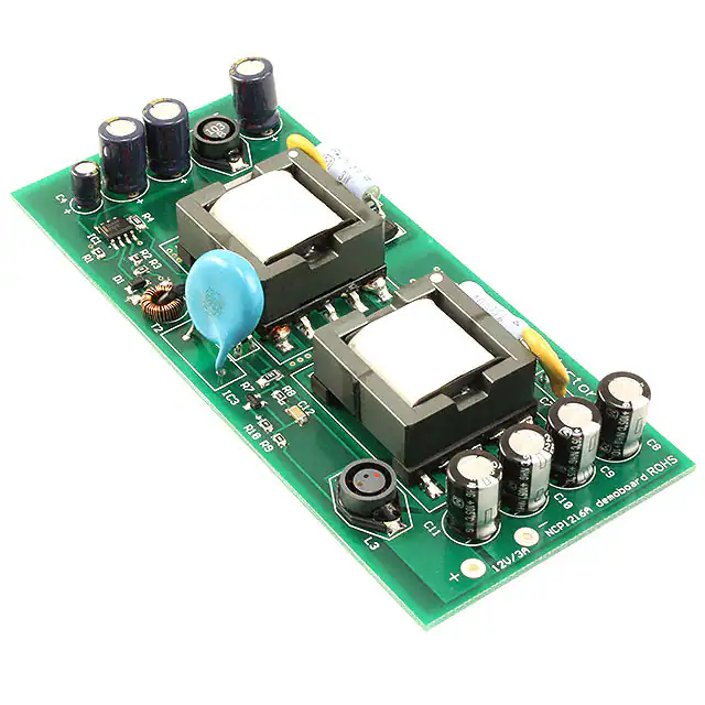
PCB Layout Design
Performance of the Converter
A double-sided PCB is used to minimize the size of the
converter. The board is designed with respect to the power
dissipation created by the power devices, thus large cooling
areas are used. Sound grounding techniques and appropriate
isolation distances were incorporated into the layout. The
PCB layout and component arrangement can be seen on
Figures 3, 4, 5 and 6.
The power conversion efficiency of the DC/DC converter
is shown in Figures 7 and 8.
86
EFFICIENCY (%)
85, 5
Table 1. BILL OF MATERIALS
L1
10 mH DS3316P−103−Coilcraft
L2
100 mH B0754−A−Coilcraft
L3
1.0 mH DS3316P−102−Coilcraft
T1
C0972−A−Coilcraft
T2
Toroid f6.0 mm, Material T30−Epcos
Ns = 38 Turns
C1, C2,
C3
22 m/100 V Nippon Chemi−Con−KMF
C4
22 m/25 V Nippon Chemi−Con−KMF
C5
1,5 nF/500 V Through Hole Ceramic Capacitor
C6
4n7 Y2 Type Capacitor
C7
2,2 nF/500 V Through Hole Ceramic Capacitor
84, 5
84
36
R1
12 kW SMD 0805
R2
1,8 kW SMD 0805
R3
10 W SMD 0805
R4
0R SMD1206
R5
8,2 kW/1.0 W Through Hole
R6
100 W/1.0 W Through Hole
R7
560 W SMD1206
R8
18 kW SMD 0805
R9
39 kW SMD 0805
R10
4,3 kW SMD 0805
D1
MMSD914T1−ON Semiconductor
D2, D3
MURA2403T3−ON Semiconductor
D4
MURB1620CT−ON Semiconductor
Q1
FQD18N20V2TF−Fairchild
IC1
NCP1216A−ON Semiconductor
IC2
PC817−SHARP
IC3
TLV431BSN1T1−ON Semiconductor
66
76
86
90
85
EFFICIENCY (%)
33 nF SMD 1206
56
Figure 7. DC/DC Converter Efficiency
vs. Input Voltage
220 m/25 V Nippon Chemi−Con−LXZ
C12
46
INPUT VOLTAGE (V)
80
75
70
65
60
0
5
10
15
20
25
OUTPUT POWER (W)
30
35
Figure 8. DC/DC Converter Efficiency
vs. Output Power (Vin = 48 V)
The no-load consumption as a function of input voltage is
shown in Figure 9.
150
NO LOAD CONSUMPTION (mW)
C8, C9,
C10, C11
85
140
130
120
110
100
90
80
70
36
40
44
48
52
56
60
64
68
72
76
80
INPUT VOLTAGE (V)
Figure 9. No Load Consumption vs. Input Voltage
http://onsemi.com
7
�NCP1216AFORWGEVB
The gate (trace 1) and drain (trace 2) waveforms of the
power MOSFET Q1 are shown in Figures 10, 11, 12 and 13
for several converter conditions.
GATE
DRAIN
GATE
DRAIN
Figure 13. Detailed Burst During Overload
The load regulation for an output current step from 10%
to 100% can be seen in Figure 14.
Figure 10. Vinput = 48 V, Iout = 3.0 A
GATE
DRAIN
Figure 14. Load Regulation (Iout changing
from 10% to 100%−0.3 A to 3.0 A)
Figure 11. No Load Operation
GATE
DRAIN
Figure 12. Overload Operation
http://onsemi.com
8
�onsemi,
, and other names, marks, and brands are registered and/or common law trademarks of Semiconductor Components Industries, LLC dba “onsemi” or its affiliates
and/or subsidiaries in the United States and/or other countries. onsemi owns the rights to a number of patents, trademarks, copyrights, trade secrets, and other intellectual property. A
listing of onsemi’s product/patent coverage may be accessed at www.onsemi.com/site/pdf/Patent−Marking.pdf. onsemi is an Equal Opportunity/Affirmative Action Employer. This
literature is subject to all applicable copyright laws and is not for resale in any manner.
The evaluation board/kit (research and development board/kit) (hereinafter the “board”) is not a finished product and is not available for sale to consumers. The board is only intended
for research, development, demonstration and evaluation purposes and will only be used in laboratory/development areas by persons with an engineering/technical training and familiar
with the risks associated with handling electrical/mechanical components, systems and subsystems. This person assumes full responsibility/liability for proper and safe handling. Any
other use, resale or redistribution for any other purpose is strictly prohibited.
THE BOARD IS PROVIDED BY ONSEMI TO YOU “AS IS” AND WITHOUT ANY REPRESENTATIONS OR WARRANTIES WHATSOEVER. WITHOUT LIMITING THE FOREGOING,
ONSEMI (AND ITS LICENSORS/SUPPLIERS) HEREBY DISCLAIMS ANY AND ALL REPRESENTATIONS AND WARRANTIES IN RELATION TO THE BOARD, ANY
MODIFICATIONS, OR THIS AGREEMENT, WHETHER EXPRESS, IMPLIED, STATUTORY OR OTHERWISE, INCLUDING WITHOUT LIMITATION ANY AND ALL
REPRESENTATIONS AND WARRANTIES OF MERCHANTABILITY, FITNESS FOR A PARTICULAR PURPOSE, TITLE, NON−INFRINGEMENT, AND THOSE ARISING FROM A
COURSE OF DEALING, TRADE USAGE, TRADE CUSTOM OR TRADE PRACTICE.
onsemi reserves the right to make changes without further notice to any board.
You are responsible for determining whether the board will be suitable for your intended use or application or will achieve your intended results. Prior to using or distributing any systems
that have been evaluated, designed or tested using the board, you agree to test and validate your design to confirm the functionality for your application. Any technical, applications or
design information or advice, quality characterization, reliability data or other services provided by onsemi shall not constitute any representation or warranty by onsemi, and no additional
obligations or liabilities shall arise from onsemi having provided such information or services.
onsemi products including the boards are not designed, intended, or authorized for use in life support systems, or any FDA Class 3 medical devices or medical devices with a similar
or equivalent classification in a foreign jurisdiction, or any devices intended for implantation in the human body. You agree to indemnify, defend and hold harmless onsemi, its directors,
officers, employees, representatives, agents, subsidiaries, affiliates, distributors, and assigns, against any and all liabilities, losses, costs, damages, judgments, and expenses, arising
out of any claim, demand, investigation, lawsuit, regulatory action or cause of action arising out of or associated with any unauthorized use, even if such claim alleges that onsemi was
negligent regarding the design or manufacture of any products and/or the board.
This evaluation board/kit does not fall within the scope of the European Union directives regarding electromagnetic compatibility, restricted substances (RoHS), recycling (WEEE), FCC,
CE or UL, and may not meet the technical requirements of these or other related directives.
FCC WARNING – This evaluation board/kit is intended for use for engineering development, demonstration, or evaluation purposes only and is not considered by onsemi to be a finished
end product fit for general consumer use. It may generate, use, or radiate radio frequency energy and has not been tested for compliance with the limits of computing devices pursuant
to part 15 of FCC rules, which are designed to provide reasonable protection against radio frequency interference. Operation of this equipment may cause interference with radio
communications, in which case the user shall be responsible, at its expense, to take whatever measures may be required to correct this interference.
onsemi does not convey any license under its patent rights nor the rights of others.
LIMITATIONS OF LIABILITY: onsemi shall not be liable for any special, consequential, incidental, indirect or punitive damages, including, but not limited to the costs of requalification,
delay, loss of profits or goodwill, arising out of or in connection with the board, even if onsemi is advised of the possibility of such damages. In no event shall onsemi’s aggregate liability
from any obligation arising out of or in connection with the board, under any theory of liability, exceed the purchase price paid for the board, if any.
The board is provided to you subject to the license and other terms per onsemi’s standard terms and conditions of sale. For more information and documentation, please visit
www.onsemi.com.
PUBLICATION ORDERING INFORMATION
LITERATURE FULFILLMENT:
Email Requests to: orderlit@onsemi.com
onsemi Website: www.onsemi.com
◊
TECHNICAL SUPPORT
North American Technical Support:
Voice Mail: 1 800−282−9855 Toll Free USA/Canada
Phone: 011 421 33 790 2910
www.onsemi.com
1
Europe, Middle East and Africa Technical Support:
Phone: 00421 33 790 2910
For additional information, please contact your local Sales Representative
�