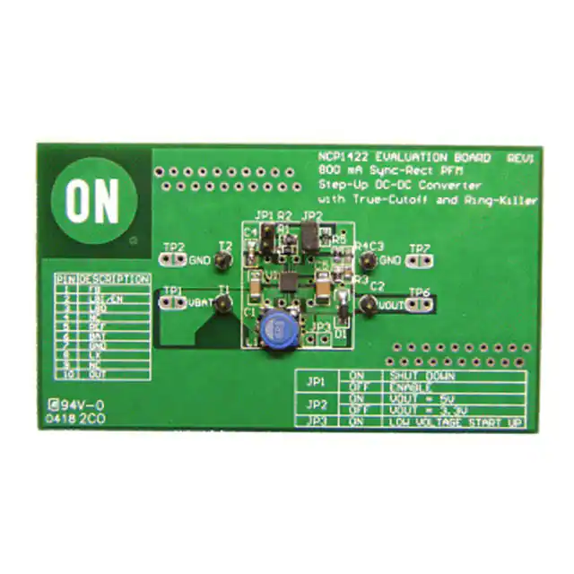
Test Procedure for the NCP1422GEVB Evaluation Board
1.
2.
3.
4.
5.
Connect the test setup as shown above.
TURN OFF the JP; (enable the device).
Set the Power Supply to 3.0V and apply to TP1, TP2, (T1, T2).
Apply 500mA loading form the electric load.
Check the input current (IIN), output voltage (VOUT) and output ripple;
For VOUT = 3.3V; JP2 OFF
IIN = 590.7mA ~ 608.7mA
VOUT = 3.267 ~ 3.367V
VRIPPLE ≤ 35mV
For VOUT = 5V; JP2 ON
IIN = 931.07mA ~ 957.4mA
VOUT = 4.859 ~ 5.0075V
VRIPPLE ≤ 40mV
6. Check the switching waveform at scope CH1 to see whether it is a normal
continuous conduction mode switching node waveform and switching ON time
(TON) is between 0.46 µs ~ 1.15 µs
6/24/2014
-1-
www.onsemi.com
�
很抱歉,暂时无法提供与“NCP1422GEVB”相匹配的价格&库存,您可以联系我们找货
免费人工找货