NCP1529ASNT1GEVB,
NCP1529MUTBGEVB
NCP1529 Series 1.7�MHz,
1�A, High Efficiency, Low
Ripple, Adjustable Output
Voltage Step-down
Converter Evaluation Board
User's Manual
http://onsemi.com
EVAL BOARD USER’S MANUAL
Overview
allowing a small inductor and capacitors. Automatic
switching PWM/PFM mode offers improved system
efficiency.
Additional features include integrated soft−start,
cycle−by−cycle current limiting and thermal shutdown
protection. The NCP1529 is available in a space saving, low
profile 2x2 x 0.5 mm UDFN6 package and TSOP−5
package.
The NCP1529 step−down DC−DC converter is a
monolithic integrated circuit for portable applications
powered from one cell Li−ion or three cell
Alkaline/NiCd/NiMH batteries.
The device – available in an adjustable output voltage
from 0.9 V to 3.9 V – is able to deliver up to 1 A. It uses
synchronous rectification to increase efficiency and reduce
external part count. The device also has a built−in 1.7 MHz
(nominal) oscillator which reduces component size by
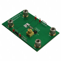
Figure 1. NCP1529ASNT1GEVB Board Picture in
TSOP−5
© Semiconductor Components Industries, LLC, 2012
April, 2012 − Rev. 1
Figure 2. NCP1529MUTBGEVB Board Picture in
UDFN−6
1
Publication Order Number:
EVBUM2106/D
�NCP1529ASNT1GEVB, NCP1529MUTBGEVB
Table 1. MAXIMUM RATINGS
Symbol
Value
Unit
Minimum Voltage All Pins
Rating
Vmin
−0.3
V
Maximum Voltage All Pins (Note 1)
Vmax
7.0
V
Maximum Voltage EN, ENI2C, SDA, SCL
Vmax
VIN + 0.3
V
Thermal Resistance, Junction−to−Air (TSOP−5 Package)
Thermal Resistance using TSOP−5 Recommended Board Layout (Note 8)
RqJA
300
110
°C/W
Thermal Resistance, Junction−to−Air (UDFN6 Package)
Thermal Resistance using UDFN6 Recommended Board Layout (Note 8)
RqJA
220
40
°C/W
Operating Ambient Temperature Range (Notes 6 and 7)
TA
−40 to 85
°C
Storage Temperature Range
Tstg
−55 to 150
°C
Junction Operating Temperature (Notes 6 and 7)
TJ
−40 to 125
°C
Latchup Current Maximum Rating (TA = 85°C) (Note 4) Other Pins
Lu
$100
mA
2.0
200
kV
V
1
per IPC
ESD Withstand Voltage (Note 3)
Human Body Model
Machine Model
Vesd
Moisture Sensitivity Level (Note 5)
MSL
Stresses exceeding Maximum Ratings may damage the device. Maximum Ratings are stress ratings only. Functional operation above the
Recommended Operating Conditions is not implied. Extended exposure to stresses above the Recommended Operating Conditions may affect
device reliability.
1. Maximum electrical ratings are defined as those values beyond which damage to the device may occur at TA = 25°C.
2. According to JEDEC standard JESD22−A108B.
3. This device series contains ESD protection and exceeds the following tests:
Human Body Model (HBM) per JEDEC standard: JESD22−A114.
Machine Model (MM) per JEDEC standard: JESD22−A115.
4. Latchup current maximum rating per JEDEC standard: JESD78.
5. JEDEC Standard: J−STD−020A.
6. In applications with high power dissipation (low VIN, high IOUT), special care must be paid to thermal dissipation issues. Board design
considerations − thermal dissipation vias, traces or planes and PCB material − can significantly improve junction to air thermal resistance
RqJA (for more information, see design and layout consideration section). Environmental conditions such as ambient temperature TA brings
thermal limitation on maximum power dissipation allowed.
The following formula gives calculation of maximum ambient temperature allowed by the application:
TA MAX = TJ MAX − (RqJA x Pd)
Where: TJ is the junction temperature,
Pd is the maximum power dissipated by the device (worst case of the application),
and RqJA is the junction−to−ambient thermal resistance.
7. To prevent permanent thermal damages, this device include a thermal shutdown which engages at 180°C (typ).
8. Board recommended TSOP−5 and UDFN−6 layouts are described on Layout Considerations section.
ELECTRICAL CHARACTERISTICS
For Electrical Characteristic, please report to our NCP1529 datasheet available on our website: http://onsemi.com.
http://onsemi.com
2
�NCP1529ASNT1GEVB, NCP1529MUTBGEVB
Table 2. NCP1529 − BOARD CONNECTIONS
Symbol
Switch Descriptions
INPUT POWER
VIN+
This is the positive connection for power supply.
VIN−
This is the return connection for the power supply
GND1, GND2
Ground clip
SETUP
ENABLE
SELECT
(UDFN package)
To enable the buck converter, connect a shorting jumper between ENABLE−1 and ENABLE−2.
To disable the buck converter, connect a shorting jumper between ENABLE−3 and ENABLE−2.
A shorting jumper must be used to select an output voltage of 1.2V or an adjustable output voltage.
OUTPUT POWER
VOUT+
This is the positive connection of the output voltage.
VOUT−
This is the return connection of the output voltage.
TEST POINT
TPVIN
This is the test point of the input voltage.
TPEN
This is the test point of the enable pin.
TPSW
This is the test point of the inductor voltage.
TPVOUT
This is the test point of the output voltage.
http://onsemi.com
3
�NCP1529ASNT1GEVB, NCP1529MUTBGEVB
NCP1529 − BOARD SCHEMATIC
VIN
VIN
ENABLE
S1
VIN+
VIN
1
CON1
VIN−
NCP1529
1
2
3
C1
10uF
1
EN
EN
VIN
EN1
EN1
1
2
0
REN
2meg
SW
3
EN
FB
5
FB
4
VIN
GND
SW
VIN
NCP1529
CON1
0
D1
FIX
0
D2
FIX
0
D3
FIX
0
LX
LX
D4
FIX
VOUT
VOUT
0
0
VOUT+
2.2mH
VOUT
0
R1
220k
FB
0
C3
18pF
1
CON1
C2
10uF
P2
1meg
VOUT−
1
0
CON1
1
GND2
JMP
0
0
0
2
GND1
JMP
2
1
0
L
1
1
1
1
SW
0
0
Figure 3. Board Schematic in TSOP−5
VIN
VIN
ENABLE
S1
VIN+
VIN
1
CON1
VIN−
C1
4.7uF
1
EN
EN
VIN
U1
1
2
3
EN
FB
1
2
0
VIN
3
FB
EN
GND
SW
VIN GND
6
EN
5
SW
4
0
NCP1529U
CON1
0
0
0
LX
LX
VOUT
VOUT
SW
L
P
1meg
GND2
JMP
CON1
C2
10uF
0
J1
CON4A
2
0
1
3
2
0
C3
18pF
0 0
Figure 4. Board Schematic in UDFN6
http://onsemi.com
4
1
VOUT−
1
CON1
2
4
GND1
JMP
1
1
R2
150k
0
VOUT
R1
150k
FB
0
VOUT+
2.2mH
0
�NCP1529ASNT1GEVB, NCP1529MUTBGEVB
NCP1529 − TEST PROCEDURE
Equipment Needed
3. Connect Vin+ to power supply and Vin− to
ground. The DC current measurement on Vin+ line
should be around 0.3 mA.
4. For the UDFN6 package, close the SELECT
connector to the potentiometer.
5. Close EN connector.
6. Modify P2 potentiometer to get Vout to 1.2 V.
Output voltage value is defined by : Vout = 0.6 x
(1 + R1/R2)
7. The DC current measurement on Vin+ line should
be around 36 mA. The part operates in PFM mode:
Power supply
Digital Volt Meter
Digital Amp Meter
Test
1. Jumper ENABLE (and SELECT for the UDFN6
package) should be open.
2. Set the power supply to 3.6 V and the current limit
of at least 1.5 A.
VSW
Vout = 1.2 V
Figure 5. VSW and Vout in PFM Mode
http://onsemi.com
5
�NCP1529ASNT1GEVB, NCP1529MUTBGEVB
8. Increase Output current to 1 A. The part works in PWM mode with a low ripple:
VSW
Vout = 1.2 V
Figure 6. VSW and Vout in PWM Mode
9. Remove J5 connector. The DC current measurement on Vp line should be back around 0.3 mA.
NCP1529 − COMPONENTS SELECTION
Input Capacitor Selection
output filter ensures good stability and fast transient
response.
Due to the nature of the buck converter, the output L−C
filter must be selected to work with internal compensation.
For NCP1529, the internal compensation is internally fixed
and it is optimized for an output filter of L = 2.2 mH and
COUT = 10 mF.
The corner frequency is given by:
In PWM operating mode, the input current is pulsating
with large switching noise. Using an input bypass capacitor
can reduce the peak current transients drawn from the input
supply source, thereby reducing switching noise
significantly. The capacitance needed for the input bypass
capacitor depends on the source impedance of the input
supply.
The maximum RMS current occurs at 50% duty cycle
with maximum output current, which is IO, max/2.
For NCP1529, a low profile ceramic capacitor of 4.7 mF
should be used for most of the cases. For effective bypass
results, the input capacitor should be placed as close as
possible to the VIN Pin
fc +
GRM188R60J475KE
4.7 mF
GRM21BR71C475KA
Taiyo Yuden
TDK
JMK212BY475MG
4.7 mF
C2012X5R0J475KT
4.7 mF
C OUT
+
1
2p Ǹ2.2 mH
10 mF
+ 34 kHz
(eq. 1)
The device operates with inductance value of 2.2 mH. If
the corner frequency is moved, it is recommended to check
the loop stability depending of the accepted output ripple
voltage and the required output current. Take care to check
the loop stability. The phase margin is usually higher than
45°.
Table 3. LIST OF INPUT CAPACITOR
Murata
1
2p ǸL
Table 4. L−C FILTER EXAMPLE
Inductance (L)
C1608X5R0J475KT
Output L−C Filter Design Considerations
The NCP1529 operates at 1.7 MHz frequency and uses
current mode architecture. The correct selection of the
http://onsemi.com
6
Output Capacitor (COUT)
2.2 mH
10 mF
4.7 mH
4.7 mF
�NCP1529ASNT1GEVB, NCP1529MUTBGEVB
Inductor Selection
Output Capacitor Selection
The inductor parameters directly related to device
performances are saturation current and DC resistance and
inductance value. The inductor ripple current (DIL)
decreases with higher inductance:
Selecting the proper output capacitor is based on the
desired output ripple voltage. Ceramic capacitors with low
ESR values will have the lowest output ripple voltage and
are strongly recommended. The output capacitor requires
either an X7R or X5R dielectric.
The output ripple voltage in PWM mode is given by:
DI L +
V OUT
L
f SW
ǒ
1*
Ǔ
V OUT
V IN
(eq. 2)
• DIL: Peak to peak inductor ripple current
• L: Inductor value
• fSW: Switching frequency
DV OUT + DI L
The saturation current of the inductor should be rated
higher than the maximum load current plus half the ripple
current:
I L(max) + I O(max) )
DI L
Murata
Taiyo Yuden
TDK
The inductor’s resistance will factor into the overall
efficiency of the converter. For best performances, the DC
resistance should be less than 0.3 W for good efficiency.
C OUT
) ESR
Ǔ
(eq. 4)
GRM188R60J475KE
4.7 mF
GRM188R60OJ106ME
10 mF
JMK212BY475MG
4.7 mF
JMK212BJ106MG
10 mF
C2012X5R0J475
4.7 muF
C1608X5R0J475
C2012X5R0J106
10 mF
Feed−Forward Capacitor Selection
Table 5. LIST OF INDUCTOR
FDK
MIPW3226 Series
TDK
VLF3010AT Series
The feed−forward capacitor sets the feedback loop
response and is critical to obtain good loop stability. Given
that the compensation is internally fixed, an 18 pF ceramic
capacitor is needed. Choose a small ceramic capacitor X7R
or X5R or COG dielectric.
TFC252005 Series
Coil Craft
1
f SW
GRM21BR71C475KA
• IL(max): Maximum inductor current
• IO(max): Maximum Output current
Taiyo Yuden
4
Table 6. LIST OF OUTPUT CAPACITOR
(eq. 3)
2
ǒ
LQ CBL2012
DO1605−T Series
LPS3008
NCP1529 − BILL OF MATERIAL
Table 7. BOM IN TSOP−5 PACKAGE
Designator
Qty
Description
Value
Tolerance
Footprint
Manufacturer
Manufacturer
Part Number
U1
1
IC, Converter,
DC/DC
NA
NA
TSOP−5
ON Semiconductor
NCP1529
C1
1
Ceramic Capacitor
4.7 mF, 6.3 V,
X5R
10%
0603
TDK
C1608X5R0J475
C2
1
Ceramic Capacitor
10 mF, 6,3 V,
X5R
10%
0603
TDK
C1608X5R0J106
C3
1
Ceramic Capacitor
18 pF, 50 V,
COG
5%
0603
TDK
C1608C0G1H180
R1
1
SMD Resistor
110k
1%
0603
std
std
P2
1
Potentiometer
1meg
10%
Vishay Spectrol
63M−T607−105
L1
1
Inductor
2,2 mH
20%
1605
Coilcraft
DO1605T−222MLB
VIN, VOUT
4
Connector
NA
NA
NA
Emerson Network
Power
Connectivity
Solutions
111−2223−001
http://onsemi.com
7
�NCP1529ASNT1GEVB, NCP1529MUTBGEVB
Table 7. BOM IN TSOP−5 PACKAGE
Designator
Qty
Description
Value
Tolerance
Footprint
Manufacturer
Manufacturer
Part Number
ENABLE
1
3 Pin Jumper
Header
NA
NA
2,54mm
TYCO/AMP
Molex/Waldom
5−826629−0
90120−0160
GND1,
GND2
2
Jumper for GND
NA
NA
10.16mm
Harwin
Molex / Waldom
D3082−01
90120−0160
EN, SW,
VIN, VOUT
4
Test Point Type 3
NA
NA
f 1.60mm
Keystone
5010
PCB
1
87 mm x 57 mm x
1.0 mm 4 Layers
NA
NA
NA
Any
TLS−P−003−A−0907
−BBR
Table 8. BOM IN UDFN−6 PACKAGE
Designator
Qty
Description
Value
Tolerance
Footprint
Manufacturer
Manufacturer
Part Number
U1
1
IC, Converter,
DC/DC
NA
NA
UDFN6
ON Semiconductor
NCP1529
C1
1
Ceramic capacitor
4.7 mF, 6.3 V,
X5R
10%
0603
TDK
C1608X5R0J475
C2
1
Ceramic capacitor
10 mF, 6.3 V,
X5R
10%
0603
TDK
C1608X5R0J106
C3
1
Ceramic capacitor
18 pF, 50 V,
COG
5%
0603
TDK
C1608C0G1H180
R1, R2
2
SMD resistor
150k
1%
0603
std
std
P2
1
Potentiometer
1meg
10%
Vishay Spectrol
63M−T607−105
L1
1
Inductor
2.2 mH
20%
1605
Coilcraft
DO1605T−222MLB
VIN, VOUT
4
Connector
NA
NA
NA
Emerson Network
Power
Connectivity
Solutions
111−2223−001
ENABLE
1
3 Pin Jumper
Header
NA
NA
2,54mm
TYCO/AMP
Molex/Waldom
5−826629−0
90120−0160
SELECT
J1
2x2 Pin Jumper
Header
NA
NA
2,54mm
TYCO/AMP
Molex/Waldom
6−166591−5
90131−0140
GND1,
GND2
2
Jumper for GND
NA
NA
10,16mm
Harwin
Molex/Waldom
D3082−01
90120−0160
EN, SW,
VIN, VOUT
4
Test point type 3
NA
NA
f
1,60mm
Keystone
5010
PCB
1
87mm x 57mm x
1.0 mm
4 Layers
NA
NA
NA
Any
TLS−P−003−A−0907
−BBR
http://onsemi.com
8
�NCP1529ASNT1GEVB, NCP1529MUTBGEVB
NCP1529 − PCB LAYOUT GUIDELINES
LAYOUT CONSIDERATIONS
Electrical Layout Considerations
participates to the good loop stability. A 18pF capacitor
is recommended to meet compensation requirements.
A four layer PCB with a ground plane and a power plane
will help NCP1529 noise immunity and loop stability.
Implementing a high frequency DC−DC converter
requires respect of some rules to get a powerful portable
application. Good layout is key to prevent switching
regulators to generate noise to application and to
themselves.
Electrical layout guide lines are:
• Use short and large traces when large amount of current
is flowing.
• Keep the same ground reference for input and output
capacitors to minimize the loop formed by high current
path from the battery to the ground plane.
• Isolate feedback pin from the switching pin and the
current loop to protect against any external parasitic
signal coupling. Add a feed−forward capacitor between
VOUT and FB which adds a zero to the loop and
Thermal Layout Considerations
High power dissipation in small package leads to thermal
consideration such as:
• Enlarge VIN trace and added several vias connected to
power plane.
• Connect GND pin to top plane.
• Join top, bottom and each ground plane together using
several free vias in order to increase radiator size.
For high ambient temperature and high power dissipation
requirements, UDFN6 package using exposed pad
connected to main radiator is recommended. Refer to
Notes 6, 7, and 8.
VOUT
Trace
EN Trace
FB Trace
VIN Trace
SW
Trace
SW
Trace
VIN Trace
FB Trace
VOUT
Trace
GND Plane
GND Plane
EN Trace
Figure 7. TSOP−5 Recommended Board Layout
Figure 8. UDFN6 Recommended Board Layout
http://onsemi.com
9
�NCP1529ASNT1GEVB, NCP1529MUTBGEVB
NCP1529 − PCB LAYOUT OF TSOP−5 DEMO BOARD
Board reference: TLS−P−003−A−0907−BBR
Figure 9. Assembly Layer in TSOP−5
Figure 10. Part Layout in TSOP−5
http://onsemi.com
10
�NCP1529ASNT1GEVB, NCP1529MUTBGEVB
Figure 11. Top Layer Routing in TSOP−5
Figure 12. Ground Layer Routing in TSOP−5
http://onsemi.com
11
�NCP1529ASNT1GEVB, NCP1529MUTBGEVB
Figure 13. Power Layer Routing in TSOP−5
Figure 14. Bottom Layer Routing in TSOP−5
http://onsemi.com
12
�NCP1529ASNT1GEVB, NCP1529MUTBGEVB
NCP1529 − PCB LAYOUT OF UDFN−6 DEMO BOARD
Board reference: TLS−P−003−A−0907−BBR
Figure 15. : Assembly Layer in UDFN6
Figure 16. Part Layout in UDFN−6
http://onsemi.com
13
�NCP1529ASNT1GEVB, NCP1529MUTBGEVB
Figure 17. Top Layer Routing in UDFN−6
Figure 18. Ground Layer Routing in UDFN6
http://onsemi.com
14
�NCP1529ASNT1GEVB, NCP1529MUTBGEVB
Figure 19. Power Layer Routing in UDFN−6
Figure 20. Bottom Layer Routing in UDFN6
http://onsemi.com
15
�onsemi,
, and other names, marks, and brands are registered and/or common law trademarks of Semiconductor Components Industries, LLC dba “onsemi” or its affiliates
and/or subsidiaries in the United States and/or other countries. onsemi owns the rights to a number of patents, trademarks, copyrights, trade secrets, and other intellectual property. A
listing of onsemi’s product/patent coverage may be accessed at www.onsemi.com/site/pdf/Patent−Marking.pdf. onsemi is an Equal Opportunity/Affirmative Action Employer. This
literature is subject to all applicable copyright laws and is not for resale in any manner.
The evaluation board/kit (research and development board/kit) (hereinafter the “board”) is not a finished product and is not available for sale to consumers. The board is only intended
for research, development, demonstration and evaluation purposes and will only be used in laboratory/development areas by persons with an engineering/technical training and familiar
with the risks associated with handling electrical/mechanical components, systems and subsystems. This person assumes full responsibility/liability for proper and safe handling. Any
other use, resale or redistribution for any other purpose is strictly prohibited.
THE BOARD IS PROVIDED BY ONSEMI TO YOU “AS IS” AND WITHOUT ANY REPRESENTATIONS OR WARRANTIES WHATSOEVER. WITHOUT LIMITING THE FOREGOING,
ONSEMI (AND ITS LICENSORS/SUPPLIERS) HEREBY DISCLAIMS ANY AND ALL REPRESENTATIONS AND WARRANTIES IN RELATION TO THE BOARD, ANY
MODIFICATIONS, OR THIS AGREEMENT, WHETHER EXPRESS, IMPLIED, STATUTORY OR OTHERWISE, INCLUDING WITHOUT LIMITATION ANY AND ALL
REPRESENTATIONS AND WARRANTIES OF MERCHANTABILITY, FITNESS FOR A PARTICULAR PURPOSE, TITLE, NON−INFRINGEMENT, AND THOSE ARISING FROM A
COURSE OF DEALING, TRADE USAGE, TRADE CUSTOM OR TRADE PRACTICE.
onsemi reserves the right to make changes without further notice to any board.
You are responsible for determining whether the board will be suitable for your intended use or application or will achieve your intended results. Prior to using or distributing any systems
that have been evaluated, designed or tested using the board, you agree to test and validate your design to confirm the functionality for your application. Any technical, applications or
design information or advice, quality characterization, reliability data or other services provided by onsemi shall not constitute any representation or warranty by onsemi, and no additional
obligations or liabilities shall arise from onsemi having provided such information or services.
onsemi products including the boards are not designed, intended, or authorized for use in life support systems, or any FDA Class 3 medical devices or medical devices with a similar
or equivalent classification in a foreign jurisdiction, or any devices intended for implantation in the human body. You agree to indemnify, defend and hold harmless onsemi, its directors,
officers, employees, representatives, agents, subsidiaries, affiliates, distributors, and assigns, against any and all liabilities, losses, costs, damages, judgments, and expenses, arising
out of any claim, demand, investigation, lawsuit, regulatory action or cause of action arising out of or associated with any unauthorized use, even if such claim alleges that onsemi was
negligent regarding the design or manufacture of any products and/or the board.
This evaluation board/kit does not fall within the scope of the European Union directives regarding electromagnetic compatibility, restricted substances (RoHS), recycling (WEEE), FCC,
CE or UL, and may not meet the technical requirements of these or other related directives.
FCC WARNING – This evaluation board/kit is intended for use for engineering development, demonstration, or evaluation purposes only and is not considered by onsemi to be a finished
end product fit for general consumer use. It may generate, use, or radiate radio frequency energy and has not been tested for compliance with the limits of computing devices pursuant
to part 15 of FCC rules, which are designed to provide reasonable protection against radio frequency interference. Operation of this equipment may cause interference with radio
communications, in which case the user shall be responsible, at its expense, to take whatever measures may be required to correct this interference.
onsemi does not convey any license under its patent rights nor the rights of others.
LIMITATIONS OF LIABILITY: onsemi shall not be liable for any special, consequential, incidental, indirect or punitive damages, including, but not limited to the costs of requalification,
delay, loss of profits or goodwill, arising out of or in connection with the board, even if onsemi is advised of the possibility of such damages. In no event shall onsemi’s aggregate liability
from any obligation arising out of or in connection with the board, under any theory of liability, exceed the purchase price paid for the board, if any.
The board is provided to you subject to the license and other terms per onsemi’s standard terms and conditions of sale. For more information and documentation, please visit
www.onsemi.com.
PUBLICATION ORDERING INFORMATION
LITERATURE FULFILLMENT:
Email Requests to: orderlit@onsemi.com
onsemi Website: www.onsemi.com
◊
TECHNICAL SUPPORT
North American Technical Support:
Voice Mail: 1 800−282−9855 Toll Free USA/Canada
Phone: 011 421 33 790 2910
www.onsemi.com
1
Europe, Middle East and Africa Technical Support:
Phone: 00421 33 790 2910
For additional information, please contact your local Sales Representative
�


 工商网监
湘ICP备2023018690号
工商网监
湘ICP备2023018690号
