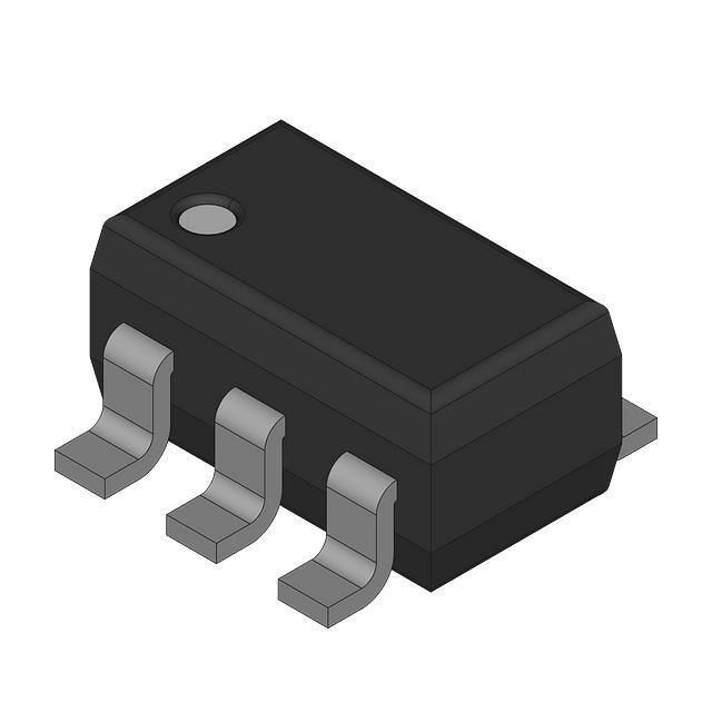
NCP1550 600 kHz PWM/PFM Step−Down DC−DC Controller
The NCP1550 is a monolithic micropower high frequency voltage mode step−down controller IC, specially designed for battery operated hand−held electronic products. With appropriate external P−type MOSFET, the device can provide up to 2.0 A loading current with high conversion efficiency. The device operates in Constant−Frequency PWM mode at normal operation, that ensures low output ripple noise, and which will automatically switch to PFM mode at low output loads for higher efficiency. Additionally, value−added features of Chip Enable to reduce IC Off−State current and integrated feedback resistor network, make it the best choice for portable applications. The device is designed to operate for voltage regulation with minimum external components and board space. This device is available in a TSOP−5 package with six standard output voltage options.
Features http://onsemi.com
1
TSOP−5 SN SUFFIX CASE 483
• High Efficiency 92%, Typical • Low Quiescent Bias Current of 50 mA • • • • • • • • • • • • • • • • • • •
(Typical at PFM Mode with No Load) Output Voltage Options from 1.8 V to 3.3 V with High Accuracy $2.0% Low Output Voltage Ripple, 50 mV, Typical PWM Switching Frequency at 600 kHz Automatic PWM/PFM Switchover at Light Load Condition Very Low Dropout Operation, 100% Max. Duty Cycle Chip Enable Pin with On−Chip 150 nA Pullup Current Source Low Shutdown Current, 0.3 mA, Typical Input Voltage Range from 2.45 V to 5.5 V Built−in Soft−Start Internal Undervoltage Lockout (UVLO) Protection Low Profile and Minimum External Components Micro Miniature TSOP−5 Package Pb−Free Packages are Available
MARKING DIAGRAM
5 xxx AYW G G 1
xxx = Specific Device Code A = Assembly Location Y = Year W = Work Week G = Pb−Free Package (Note: Microdot may be in either location)
PIN CONNECTIONS
CE GND VOUT 1 2 3 (Top View) 4 EXT 5 VIN
Typical Applications
Personal Digital Assistant (PDA) Camcorders and Digital Still Camera Hand−Held Instrument Distributed Power System Computer Peripheral Conversion from Four NiMH or NiCd or One Lithium−ion Cells to 3.3 V/1.8 V
ORDERING INFORMATION
See detailed ordering and shipping information in the package dimensions section on page 16 of this data sheet.
© Semiconductor Components Industries, LLC, 2006
1
July, 2006 − Rev. 8
Publication Order Number: NCP1550/D
�NCP1550
+ CP1 PWM Controller −
UVLO 5 VIN
2.2 V
+ −
VOUT
3 A1 − +
TON t TON(PFM)
600 kHz Oscillator
Driver
4
EXT
Voltage Reference and Soft−Start GND 2 M1
1
CE
Figure 1. Simplified Block Diagram PIN FUNCTION DESCRIPTIONS
Pin 1 2 3 4 5 Symbol CE GND VOUT EXT VIN Description Chip Enable pin, active high (internal pullup current source). By connecting this pin to GND, the switching operation of the controller will be stopped. Ground Connection Output voltage monitoring input. This pin must be connected to the regulated output node as a feedback to on−chip control circuitry. VOUT is internally connected to the on−chip voltage divider that determines the output voltage level. Gate drive for external P−MOSFET Power supply input
MAXIMUM RATINGS (TA = 25°C unless otherwise noted)
Rating Device Power Supply, VIN (Pin 5) Input/Output Pins CE (Pin 1) VOUT (Pin 3) EXT (Pin 4) Thermal Characteristics TSOP−5 Plastic Package, Case 483−01 Thermal Resistance, Junction−to−Air Operating Junction Temperature Range Operating Ambient Temperature Range Storage Temperature Range Symbol VIN VCE VOUT VEXT RqJA Value −0.3 to 6.0 −0.3 to 6.0 −0.3 to 6.0 −0.3 to 6.0 250 °C/W Unit V V
TJ TA Tstg
−40 to +150 −40 to +85 −55 to +150
°C °C °C
Stresses exceeding Maximum Ratings may damage the device. Maximum Ratings are stress ratings only. Functional operation above the Recommended Operating Conditions is not implied. Extended exposure to stresses above the Recommended Operating Conditions may affect device reliability. NOTE: ESD data available upon request. 1. This device series contains ESD protection and exceeds the following tests: Human Body Model (HBM) $2.0 kV per JEDEC standard: JESD22−A114. Machine Model (MM) $200V per JEDEC standard: JESD22−A115. 2. Latchup Current Maximum Rating: 150 mA per JEDEC standard: JESD78. 3. Moisture Sensitivity Level (MSL): 1 per IPC/JEDEC standard: J−STD−020A.
http://onsemi.com
2
�NCP1550
ELECTRICAL CHARACTERISTICS (VIN = 5.0 V, TA = 25°C for typical value, −40°C v TA v 85°C for min/max values unless
otherwise noted.) Characteristic TOTAL DEVICE Input Voltage Output Voltage (ILOAD = 0 mA, TA = 25°C) NCP1550SN18T1 NCP1550SN19T1 NCP1550SN25T1 NCP1550SN27T1 NCP1550SN30T1 NCP1550SN33T1 Input Current into VOUT Pin NCP1550SN18T1 NCP1550SN19T1 NCP1550SN25T1 NCP1550SN27T1 NCP1550SN30T1 NCP1550SN33T1 Temperature Coefficient Operating Current (VIN = 5.0 V, VCE = 5.0 V, No External Components) NCP1550SN18T1 NCP1550SN19T1 NCP1550SN25T1 NCP1550SN27T1 NCP1550SN30T1 NCP1550SN33T1 Off−State Current (VIN = 5.0 V, VCE = 0 V, TA = 25°C) NCP1550SN18T1 NCP1550SN19T1 NCP1550SN25T1 NCP1550SN27T1 NCP1550SN30T1 NCP1550SN33T1 OSCILLATOR Frequency Frequency Temperature Coefficient (TA = −40°C to 85°C) Maximum Duty Cycle PWM/PFM Switchover ON Time Threshold (Note 4) Soft−Start Delay Time (Note 4) Protection Delay Time (Auto Restart) OUTPUT DRIVE (PIN 4) EXT “H” Output Current (VEXT = VIN – 0.4 V) EXT “L” Output Current (VEXT = 0.4 V) EXT “L−H” Rise Time (CLOAD = 1000 pF) (VIN = 5.0 V) EXT “H−L” Fall Time (CLOAD = 1000 pF) (VIN = 5.0 V) EXT “L−H” Rise Time (CLOAD = 5.0 nF) (VIN = 5.0 V) EXT “H−L” Fall Time (CLOAD = 5.0 nF) (VIN = 5.0 V) 4. PWM/PFM Switchover ON Time Threshold min/max guaranteed by design only. IEXTH IEXTL Tr Tf Tr Tf − − − − − − −60 100 65 40 140 90 − − − − − − mA mA ns ns ns ns FOSC DFOSC/DTA DMAX TON(PFM) Tss Tprot 510 − 100 167 − − 600 0.11 − 320 8.0 8.0 690 − − 500 − − kHz %/°C % ns ms ms VIN VOUT 1.764 1.862 2.450 2.646 2.940 3.234 IVOUT − − − − − − DVOUT/DVT IDD − − − − − − IOFF − − − − − − 0.3 0.3 0.3 0.3 0.3 0.3 0.5 0.5 0.5 0.5 0.5 0.5 50 50 50 50 50 50 80 80 80 80 80 80 mA − 2.5 2.5 2.5 2.5 2.5 2.5 100 4.0 4.0 4.0 4.0 4.0 4.0 − ppm/°C mA 1.8 1.9 2.5 2.7 3.0 3.3 1.836 1.938 2.550 2.754 3.060 3.366 mA 2.45 − 5.50 V V Symbol Min Typ Max Unit
http://onsemi.com
3
�NCP1550
ELECTRICAL CHARACTERISTICS (continued) (VIN = 5.0 V, TA = 25°C for typical value, −40°C v TA v 85°C for min/max values
unless otherwise noted.) Characteristic CE (PIN 1) CE “H” Input Voltage CE “L” Input Voltage CE “H” Input Current (VIN = VCE = 5.0 V) CE “L” Input Current (VIN = 5.0, VCE = 0 V) Undervoltage Lockout Undervoltage Lockout Threshold Undervoltage Lockout Hysteresis VUVLO VUVLO_HYS 1.60 − 2.20 50 2.40 − V mV VCEH VCEL ICEH ICEL 1.3 − −0.5 −0.5 − − 0 0.15 − 0.3 0.5 0.5 V V mA mA Symbol Min Typ Max Unit
L VIN M VOUT
SD
CIN
VIN
EXT
COUT
5
1
2
CE CE
3
4 GND
VOUT
GND
GND
Figure 2. Typical Application Diagram
http://onsemi.com
4
�NCP1550
TYPICAL OPERATING CHARACTERISTICS
100 VIN = 4.0 V 80 EFFICIENCY (%) EFFICIENCY (%) 5.0 V NCP1550SN33T1 L = 3.3 mH CIN = 33 mF COUT = 33 mF M = NTGS3441T1 SD = MBRM120LT3 1 10 100 1000 80 4.0 V 5.0 V 60 NCP1550SN25T1 L = 5.6 mH CIN = 33 mF COUT = 33 mF M = NTGS3441T1 SD = MBRM120LT3 1 10 100 1000 100 VIN = 3.0 V
60
40
40
20 0
20 0
ILOAD, OUTPUT LOADING CURRENT (mA)
ILOAD, OUTPUT LOADING CURRENT (mA)
Figure 3. Efficiency versus Load Current
Figure 4. Efficiency versus Load Current
100 VIN = 3.0 V 80 EFFICIENCY (%) 5.0 V NCP1550SN18T1 L = 6.8 mH CIN = 33 mF COUT = 33 mF M = NTGS3441T1 SD = MBRM120LT3 1 10 100 1000 4.0 V
60
40
20
0 ILOAD, OUTPUT LOADING CURRENT (mA)
Figure 5. Efficiency versus Load Current
http://onsemi.com
5
�NCP1550
TYPICAL OPERATING CHARACTERISTICS
DVOUT, OUTPUT VOLTAGE CHANGE (%) 0.9 VRIPPLE, RIPPLE VOLTAGE (mVp−p) 0.6 0.3 0 −0.3 −0.6 −0.9 10 100 ILOAD, OUTPUT LOADING CURRENT (mA) 1000 2.7 V 3.0 V VIN = 5.0 V CIN = 33 mF COUT = 33 mF M = NTGS3441T1 SD = MBRM120LT3 1.8 V 1.9 V 2.5 V 100 NCP1550 CIN = 33 mF COUT = 33 mF IOUT = 500 mA SD = MBRM120LT3 2.7 V 40 3.3 V 3.0 V
80
60
3.3 V
20 1.8 V 1.9 V 0 2 2.5 3 3.5 4 4.5 5 5.5 VIN, BATTERY INPUT VOLTAGE (V) 2.5 V
Figure 6. Output Voltage Change versus Load Current
IBATT, NO LOAD OPERATING CURRENT (mA) 100 DVOUT, OUTPUT VOLTAGE CHANGE (mV) 0.9 0.6 0.3 0 −0.3 −0.6 −0.9 2
Figure 7. Output Ripple Voltage versus Input Voltage
80 2.5 V 60 1.9 V
1.8 V
1.8 V
1.9 V 2.5 V
40 3.3 V 20 3.0 V 2.7 V NCP1550 CIN = 33 mF COUT = 33 mF CE = VIN SD = MBRM120LT3 4 4.5 5 5.5
NCP1550 VIN = 5.0 V CIN = 33 mF COUT = 33 mF IOUT = 500 mA SD = MBRM120LT3 2.5 3 3.5
2.7 V
3.0 V
3.3 V
0 2 2.5 3 3.5
4
4.5
5
5.5
VIN, INPUT VOLTAGE (V)
VIN, INPUT VOLTAGE (V)
Figure 8. No Load Operating Current versus Input Voltage
Figure 9. Output Voltage Change versus Input Voltage
VRIPPLE, RIPPLE VOLTAGE (mVp−p)
90 75 60 45 30 15 0 1 10 2.5 V 1.8 V 100 1000 1.9 V NCP1550 VIN = 5.0 V CIN = 33 mF COUT = 33 mF IOUT = 500 mA SD = MBRM120LT3 3.3 V
3.0 V
2.7 V
ILOAD, OUTPUT CURRENT (mA)
Figure 10. Output Ripple Voltage versus Output Current
http://onsemi.com
6
�NCP1550
(VIN = 5.0 V, ILOAD = 500 mA, L = 3.3 mH, COUT = 100 mF) Upper Trace: Output Voltage Ripple, 50 mV/Division Middle Trace: Inductor Current, IL, 500 mA/Division Lower Trace: Voltage at Cathode of Schottky Diode, 2.0 V/Division
(VIN = 5.0 V, ILOAD = 100 mA, L = 3.3 mH, COUT = 100 mF) Upper Trace: Output Voltage Ripple, 50 mV/Division Middle Trace: Inductor Current, IL, 500 mA/Division Lower Trace: Voltage at Cathode of Schottky Diode, 2.0 V/Division
Figure 11. Continuous Conduction Mode PWM Switching Waveform for VOUT = 3.3 V
Figure 12. Discontinuous Conduction Mode PWM Switching Waveform for VOUT = 3.3 V
(VIN = 5.0 V, ILOAD = 10 mA, L = 3.3 mH, COUT = 100 mF) Upper Trace: Output Voltage Ripple, 50 mV/Division Middle Trace: Inductor Current, IL, 500 mA/Division Lower Trace: Voltage at Cathode of Schottky Diode, 2.0 V/Division
(VIN = 5.0 V, ILOAD = 500 mA, L = 5.6 mH, COUT = 33 mF) Upper Trace: Output Voltage Ripple, 50 mV/Division Middle Trace: Inductor Current, IL, 500 mA/Division Lower Trace: Voltage at Cathode of Schottky Diode, 2.0 V/Division
Figure 13. Discontinuous Conduction Mode PFM Switching Waveform for VOUT = 3.3 V
Figure 14. Continuous Conduction Mode PWM Switching Waveform for VOUT = 2.5 V
http://onsemi.com
7
�NCP1550
(VIN = 5.0 V, ILOAD = 100 mA, L = 5.6 mH, COUT = 33 mF) Upper Trace: Output Voltage Ripple, 50 mV/Division Middle Trace: Inductor Current, IL, 500 mA/Division Lower Trace: Voltage at Cathode of Schottky Diode, 2.0 V/Division
(VIN = 5.0 V, ILOAD = 30 mA, L = 5.6 mH, COUT = 33 mF) Upper Trace: Output Voltage Ripple, 50 mV/Division Middle Trace: Inductor Current, IL, 500 mA/Division Lower Trace: Voltage at Cathode of Schottky Diode, 2.0 V/Division
Figure 15. Discontinuous Conduction Mode PWM Switching Waveform for VOUT = 2.5 V
Figure 16. Discontinuous Conduction Mode PFM Switching Waveform for VOUT = 2.5 V
(VIN = 5.0 V, ILOAD = 500 mA, L = 6.8 mH, COUT = 33 mF) Upper Trace: Output Voltage Ripple, 50 mV/Division Middle Trace: Inductor Current, IL, 500 mA/Division Lower Trace: Voltage at Cathode of Schottky Diode, 2.0 V/Division
(VIN = 5.0 V, ILOAD = 60 mA, L = 6.8 mH, COUT = 33 mF) Upper Trace: Output Voltage Ripple, 50 mV/Division Middle Trace: Inductor Current, IL, 500 mA/Division Lower Trace: Voltage at Cathode of Schottky Diode, 2.0 V/Division
Figure 17. Continuous Conduction Mode PWM Switching Waveform for VOUT = 1.8 V
Figure 18. Discontinuous Conduction Mode PWM Switching Waveform for VOUT = 1.8 V
http://onsemi.com
8
�NCP1550
(VIN = 5.0 V, ILOAD = 30 mA, L = 6.8 mH, COUT = 33 mF) Upper Trace: Output Voltage Ripple, 50 mV/Division Middle Trace: Inductor Current, IL, 500 mA/Division Lower Trace: Voltage at Cathode of Schottky Diode, 2.0 V/Division Upper Trace: Input Voltage, 2.0 V/Division Lower Trace: Output Voltage, 2.0 V/Division
Figure 19. Discontinuous Conduction Mode PFM Switching Waveform for VOUT = 1.8 V
Figure 20. Startup Transient Response for VOUT = 3.3 V
Upper Trace: Input Voltage, 2.0 V/Division Lower Trace: Output Voltage, 1.0 V/Division
Upper Trace: Output Voltage Waveform, 2.0 V/Division Lower Trace: Chip Enable/Disable Pin Waveform, 0.5 V/Division
Figure 21. Startup Transient Response for VOUT = 1.8 V
Figure 22. Chip Enable/Disable Output Voltage Waveform
http://onsemi.com
9
�NCP1550
(VIN = 4.0 to 5.0 V, L = 3.3 mH, COUT = 33 mF, ILOAD = 1.0 A) Upper Trace: Output Voltage Ripple, 100 mV/Division Lower Trace: Input Voltage, 2.0 V/Division
(VIN = 3.0 to 5.0 V, L = 5.6 mH, COUT = 33 mF, ILOAD = 1.0 A) Upper Trace: Output Voltage Ripple, 100 mV/Division Lower Trace: Input Voltage, 2.0 V/Division
Figure 23. Line Transient Response for VOUT = 3.3 V
Figure 24. Line Transient Response for VOUT = 2.5 V
(VIN = 3.0 to 5.0 V, L = 6.8 mH, COUT = 33 mF, ILOAD = 1.0 A) Upper Trace: Output Voltage Ripple, 100 mV/Division Lower Trace: Input Voltage, VIN, 2.0 V/Division
(VIN = 5.0 V, ILOAD = 100 mA to 1.0 A, L = 3.3 mH, COUT = 33 mF) Upper Trace: Output Voltage Ripple, 200 mV/Division Lower Trace: Load Current, ILOAD, 500 mA/Division
Figure 25. Line Transient Response for VOUT = 1.8 V
Figure 26. Load Transient Response for VOUT = 3.3 V
http://onsemi.com
10
�NCP1550
(VIN = 5.0 V, ILOAD = 100 mA to 1.0 A, L = 5.6 mH, COUT = 33 mF) Upper Trace: Output Voltage Ripple, 100 mV/Division Lower Trace: Load Current, ILOAD, 500 mA/Division
(VIN = 5.0 V, ILOAD = 100 mA to 1.0 A, L = 6.8 mH, COUT = 33 mF) Upper Trace: Output Voltage Ripple, 100 mV/Division Lower Trace: Load Current, ILOAD, 500 mA/Division
Figure 27. Load Transient Response for VOUT = 2.5 V
2.0 IOFF, OFF−STATE CURRENT (mA) IDD, OPERATING CURRENT (mA) 70
Figure 28. Load Transient Response for VOUT = 1.8 V
1.6
3.3 V
60
1.2
2.5 V
50 2.5 V 40 VIN = 5.0 V VCE = 5.0 V 3.3 V 1.8 V
0.8 1.8 V 0.4
30 20 −50
0 −50
−25
0
25
50
75
100
−25
0
25
50
75
100
TA, AMBIENT TEMPERATURE (°C)
TA, AMBIENT TEMPERATURE (°C)
Figure 29. Off−Stage Current versus Ambient Temperature
FOSC, OSCILLATOR FREQUENCY (kHz) 700 2.5 V 1.8 V TON(PFM), PWM/PFM SWITCH ON TIME THRESHOLD (ns) 450
Figure 30. Operating Current versus Ambient Temperature
650
400 3.3 V
600
350
2.5 V
550
3.3 V
300 1.8 V VIN = 5.0 V 200 −50 −25 0 25 50 75 TA, AMBIENT TEMPERATURE (°C) 100
500 VIN = 5.0 V 450 −50 −25 0 25 50 75 TA, AMBIENT TEMPERATURE (°C) 100
250
Figure 31. Oscillator Frequency versus Ambient Temperature
Figure 32. PWM/PFM Switch ON Time Threshold versus Ambient Temperature
http://onsemi.com
11
�NCP1550
3.35 VOUT, OUTPUT VOLTAGE (V) VOUT, OUTPUT VOLTAGE (V) 2.55
3.33
2.53
3.31
2.51
3.29 VIN = 5.0 V 3.27 3.25 −50
2.49 VIN = 5.0 V 2.47 2.45 −50
−25
0
25
50
75
100
−25
0
25
50
75
100
TA, AMBIENT TEMPERATURE (°C)
TA, AMBIENT TEMPERATURE (°C)
Figure 33. NCP1550SN33T1 Output Voltage versus Ambient Temperature
Figure 34. NCP1550SN25T1 Output Voltage versus Ambient Temperature
IEXTH, EXT “H” OUTPUT CURRENT (mA)
1.85 VOUT, OUTPUT VOLTAGE (V)
−40 −50 −60 −70 −80 −90 −100 −50 VEXT = VIN − 0.4 V VIN = 5.0 V −25 0 25 50 75 100 2.5 V 3.3 V 1.8 V
1.83
1.81
1.79 VIN = 5.0 V 1.77 1.75 −50
−25
0
25
50
75
100
TA, AMBIENT TEMPERATURE (°C)
TA, AMBIENT TEMPERATURE (°C)
Figure 35. NCP1550SN18T1 Output Voltage versus Ambient Temperature
Figure 36. NCP1550 EXT “H” Output Current versus Ambient Temperature
IVOUT, INPUT CURRENT INTO VOUT PIN (mA)
IEXTH, EXT “L” OUTPUT CURRENT (mA)
200
3.5 VIN = 5.0 V 3.0 2.5 V 2.5 1.8 V 2.0 3.3 V 1.5 −50 −25 0 25 50 75 100
170 2.5 V 3.3 V 1.8 V VEXT = 0.4 V VIN = 5.0 V
140
110
80 50 −50
−25
0
25
50
75
100
TA, AMBIENT TEMPERATURE (°C)
TA, AMBIENT TEMPERATURE (°C)
Figure 37. NCP1550 EXT “L” Output Current versus Ambient Temperature
Figure 38. NCP1550 Input Current into VOUT Pin versus Ambient Temperature
http://onsemi.com
12
�NCP1550
DETAILED OPERATING DESCRIPTION
Detailed Operating Description
The NCP1550 series are step−down (Buck) DC−DC controllers designed primarily for use in portable applications powered by battery cells. With an appropriate external P−channel MOSFET connected, the device can provide up to 2 A loading current with high conversion efficiency. The NCP1550 series using an unique control scheme combines the advantages of Pulse−Frequency− Modulation (PFM) that can provide excellent efficiency even at light loading conditions and Constant−Frequency Pulse−Width−Modulation that can achieve high efficiency and low output voltage ripple at heavy loads. The NCP1550 working at high switching frequency makes it possible to use small size surface mount inductor and capacitors to reduce PCB area and provide better interference handling for noise sensitive applications. The simplified functional blocks of the device are shown in Figure 1 and descriptions for each of the functions are given below.
The Internal Oscillator
voltage at its output. This error voltage is compared with the ramp function to generate the control pulse to drive the external power switch. On a cycle−by−cycle basis, the greater the error voltage, the longer the switch is held on. Hence, corresponding corrective action will be made to keep the output voltage within regulation. Constant−Frequency PWM reduces output voltage ripple and noise, which is one of the important characteristics for noise sensitive communication applications. The high switching frequency allows small size surface mount components to improve layout compactness and reduce PC board area, and eliminate audio and emission interference.
Power−Saving Pulse−Frequency−Modulation (PFM) Control Scheme
An oscillator that governs the switching of a PWM control cycles is required. NCP1550 have an internal Fixed− Frequency oscillator. The oscillator frequency is trimmed to 600 kHz with an accuracy of ±15%. All other timing signals needed for operation are derived from this oscillator signal.
Voltage Reference and Soft−Start
An internal high accuracy voltage reference is included in NCP1550. This reference voltage is connected to the inverting input terminal of the error amplifier, A1, which compared with portion of the output voltage, VOUT derived from an integrated voltage divider with precise trimming to give the required output voltage at ±2% accuracy. NCP1550 also comes with a built−in soft−start circuit that controls the ramping up of the internal reference voltage during the power−up of the converter. This function effectively enables the output voltage to rise gradually over the specified soft−start time, 8 msec typical. This prevents the output voltage from overshooting during startup of the converter.
Voltage Mode Pulse−Width−Modulation (PWM) Control Scheme
While the loading is decreasing, the converter enters the Discontinuous Conduction Mode (DCM) operation, which means the inductor current will decrease to zero before the next switching cycle starts. In DCM operation, the ON time for each switching cycle will decrease significantly when the output current decreases. In order to maintain a high conversion efficiency even at light load conditions, the ON time for each switching cycle is closely monitored and for any ON time smaller than the preset value, 320 nsec, the switching pulse will be skipped. As a result, when the loading current is small, the converter will be operating in a “Constant ON time (320 nsec nominal), variable OFF time” Pulse−Frequency Modulation (PFM) mode. This innovative control scheme improves the conversion efficiency for the system at light load and standby operating conditions hence extend the operating life of the battery.
Low Power Shutdown Mode
NCP1550 can be disabled whenever the CE pin (Pin 1) is tied to GND. In shutdown, the internal reference, oscillator, control circuitry, driver and internal feedback voltage divider are turned off and the output voltage falls to 0 V. During the shutdown mode, as most of the internal functions are stopped and current paths are cut−off, the device consume extremely small current in this condition.
Under−Voltage Lockout (UVLO)
For normal operation, NCP1550 is working in Constant−Frequency Pulse−Width−Modulation (PWM) Voltage Mode Control. The controller operates with the internal oscillator, which generates the required ramp function to compare with the output of the error amplifier, A1. The error amplifier compares the internally divided−down output voltage with the voltage reference to produce an error
To prevent operation of the P−Channel MOSFET below safe input voltage levels, an Undervoltage Lockout is incorporated into the NCP1550. When the input supply voltage drops below approximately 2.2 V, the comparator, CP1 will turn−off the control circuitry and shut the converter down.
http://onsemi.com
13
�NCP1550
APPLICATIONS INFORMATION
Inductor Value Calculation
Selecting the proper inductance is a trade−off between inductor’s physical size, transient respond and power conversion requirements. Lower value inductor saves cost, PC board space and providing faster transient response, but result in higher ripple current and core losses. Considering an application with loading current, IOUT = 0.5 A and the inductor ripple current, IL−RIPPLE(P−P) is designed to be less than 40% of the load current, i.e. 0.5 A x 40% = 0.2 A. The relationship between the inductor value and inductor ripple current is given by,
T * (VIN * RDS(ON) IOUT * VOUT) L + ON IL*RIPPLE(P*P)
(eq. 1)
P−Channel switch duty cycle. At high input voltages, the diode conducts most of the time. In case of VIN approaches VOUT, the diode conducts only a small fraction of the cycle. While the output terminals are shorted, the diode will subject to its highest stress. Under this condition, the diode must be able to safely handle the peak current circulating in the loop. So, it is important to select a flywheel diode that can meet the diode peak current and average power dissipation requirements. Under normal conditions, the average current conducted by the flywheel diode is given by:
ID + VIN * VOUT VIN ) VF IOUT
(eq. 2)
Where RDS(ON) is the ON resistance of the external P−channel MOSFET. Figure 39 is a plot for recommended inductance against nominal input voltage for different output options.
12 RDS(ON) = 0.1 W 10 L, INDUCTANCE (mH) 2.5 V 8 6 4 2 2.7 V 0 2.2 2.7 3.2 3.7 4.2 4.7 5.2 3.0 V 1.8 V 1.9 V
Where ID is the average diode current and VF is the forward diode voltage drop. A fast switching diode must also be used to optimize efficiency. Schottky diodes are a good choice for low forward drop and fast switching times.
Input and Output Capacitor Selection (CIN and COUT)
In continuous mode operation, the source current of the P−Channel MOSFET is a square wave of duty cycle (VOUT + VF)/VIN. To prevent large input voltage transients, a low ESR input capacitor that can support the maximum RMS input current must be selected. The maximum RMS input current, IRMS(MAX) can be estimated by the equation in below:
3.3 V
IRMS(MAX) [ IOUT
VOUT(VIN * VOUT) 2 VIN
1
(eq. 3)
VIN, INPUT VOLTAGE OF NCP1550 (V)
Figure 39. Inductor Selection Chart P−Channel Power MOSFET Selection
Above estimation has a maximum value at VIN = 2VOUT, where IRMS(MAX) = IOUT/2. As a general practice, this simple worst−case condition is used for design. Selection of the output capacitor, COUT is primarily governed by the required effective series resistance (ESR) of the capacitor. Typically, once the ESR requirement is met, the capacitance will be adequate for filtering. The output voltage ripple, VRIPPLE is approximated by:
VRIPPLE [ IL * RIPPLE(P*P) (ESR )
(eq. 4) 1 ) 4 FOSCCOUT
An external P−Channel power MOSFET must be used with the NCP1550. The key selection criteria for the power MOSFET are the gate threshold, VGS, the “ON” resistance, RDS(ON) and its total gate charge, QT. For low input voltage operation, we need to select a low gate threshold device that can work down to the minimum input voltage level. RDS(ON) determines the conduction losses for each switching cycle, the lower the ON resistance, the higher the efficiency can be achieved. A power MOSFET with lower gate charge can give lower switching losses but the fast transient can cause unwanted EMI to the system. Compromise in between is required during the design stage. For 1.0 A and 2.0 A load current, NTGS3441T1 and NTGS3443T1 are tested to be appropriate for most applications.
Flywheel Diode Selection
Where FOSC is the switching frequency and ESR is the effective series resistance of the output capacitor. From equation (4), it can be noted that the output voltage ripple contributed by two parts. For most of the case, the major contributor is the capacitor ESR. Ordinary aluminum−electrolytic capacitors have high ESR and should be avoided. Higher quality Low ESR aluminum−electrolytic capacitors are acceptable and relatively inexpensive. For even better performance, Low ESR tantalum capacitors should be used. Surface−mount tantalum capacitors are better and provide neat and compact solution for space sensitive applications.
The flywheel diode is turned on and carries load current during the off time. The average diode current depends on the
http://onsemi.com
14
�NCP1550
PCB Layout Recommendations Good PCB layout plays an important role in switching mode power conversion. Careful PCB layout can help to minimize ground bounce, EMI noise and unwanted feedbacks that can affect the performance of the converter. Suggested hints below can be used as a guideline in most situations.
Grounding Components Placement
Power components, i.e. input capacitor, inductor and output capacitor, must be placed as close together as possible. All connecting traces must be short, direct and thick. High current flowing and switching paths must be kept away from the feedback (VOUT, pin 3) terminal to avoid unwanted injection of noise into the feedback path.
Feedback Path
Star−ground connection should be used to connect the output power return ground, the input power return ground and the device power ground together at one point. All high current running paths must be thick enough for current flowing through and producing insignificant voltage drop along the path. Feedback signal path must be separated from the main current path and sensing directly at the anode of the output capacitor.
External Component Reference Data
Inductor (L) 6.8 mH
Feedback of the output voltage must be a separate trace separated from the power path. The output voltage sensing trace to the feedback (VOUT, pin 3) pin should be connected to the output voltage directly at the anode of the output capacitor.
Device NCP1550SN18T1
VOUT 1.8 V
Inductor Model CDD5D23 6R8 (1A) CDRH6D38 6R8 (2A) Sumida CDC5D23 6R8 (1A) CDRH6D38 6R8 (2A) Sumida CDC5D23 5R6 (1A) CDRH6D38 5R0 (2A) Sumida CDC5D23 5R6 (1A) CDRH6D38 5R0 (2A) Sumida CDC5D23 4R7 (1A) CDRH6D28 5R0 (2A) Sumida CD43 3R3 (1A) CDRH6D38 3R3 (2A) Sumida
External MOSFET (M) NTGS3441T1 (1A) NTGS3443T1 (2A) ON Semiconductor NTGS3441T1 (1A) NTGS3443T1 (2A) ON Semiconductor NTGS3441T1 (1A) NTGS3443T1 (2A) ON Semiconductor NTGS3441T1 (1A) NTGS3443T1 (2A) ON Semiconductor NTGS3441T1 (1A) NTGS3443T1 (2A) ON Semiconductor NTGS3441T1 (1A) NTGS3443T1 (2A) ON Semiconductor
Diode (SD) MBRM120LT3 ON Semiconductor
Output and Input Capacitor COUT/CIN 33 mF/33 mF (1A) 68 mF/33 mF (2A) KEMET (T494 series) 33 mF/33 mF (1A) 68 mF/33 mF (2A) KEMET (T494 series) 33 mF/33 mF (1A) 68 mF/33 mF (2A) KEMET (T494 series) 33 mF/33 mF (1A) 68 mF/33 mF (2A) KEMET (T494 series) 33 mF/33 mF (1A) 68 mF/33 mF (2A) KEMET (T494 series) 68 mF/33 mF (1A) 100 mF/68 mF (2A) KEMET (T494 series)
NCP1550SN19T1
1.9 V
6.8 mH
MBRM120LT3 ON Semiconductor
NCP1550SN25T1
2.5 V
5.6 mH 5.0 mH
MBRM120LT3 ON Semiconductor
NCP1550SN27T1
2.7 V
5.6 mH 5.0 mH
MBRM120LT3 Semiconductor
NCP1550SN30T1
3.0 V
5.6 mH 5.0 mH
MBRM120LT3 ON Semiconductor
NCP1550SN33T1
3.3 V
3.3 mH
MBRM120LT3 ON Semiconductor
http://onsemi.com
15
�NCP1550
ORDERING INFORMATION
Part Number NCP1550SN33T1 NCP1550SN33T1G NCP1550SN30T1 NCP1550SN30T1G NCP1550SN27T1 NCP1550SN27T1G NCP1550SN25T1 NCP1550SN25T1G NCP1550SN19T1 NCP1550SN19T1G NCP1550SN18T1 NCP1550SN18T1G Output Voltage (VOUT) 3.3 V 3.3 V 3.0 V 3.0 V 2.7 V 2.7 V 600 kHz 2.5 V 2.5 V 1.9 V 1.9 V 1.8 V 1.8 V DCA DCA DBE DBE DBZ DBZ TSOP−5 TSOP−5 (Pb−Free) TSOP−5 TSOP−5 (Pb−Free) TSOP−5 TSOP−5 (Pb−Free) Switching Frequency Device Marking DCD DCD DBF DBF DCB DCB Package TSOP−5 TSOP−5 (Pb−Free) TSOP−5 TSOP−5 (Pb−Free) TSOP−5 TSOP−5 (Pb−Free) 3000 Tape & Reel Shipping†
†For information on tape and reel specifications, including part orientation and tape sizes, please refer to our Tape and Reel Packaging Specifications Brochure, BRD8011/D.
http://onsemi.com
16
�NCP1550
PACKAGE DIMENSIONS
THIN SOT23−5/TSOP−5/SC59−5 SN SUFFIX CASE 483−02 ISSUE F
NOTES: 1. DIMENSIONING AND TOLERANCING PER ASME Y14.5M, 1994. 2. CONTROLLING DIMENSION: MILLIMETERS. 3. MAXIMUM LEAD THICKNESS INCLUDES LEAD FINISH THICKNESS. MINIMUM LEAD THICKNESS IS THE MINIMUM THICKNESS OF BASE MATERIAL. 4. DIMENSIONS A AND B DO NOT INCLUDE MOLD FLASH, PROTRUSIONS, OR GATE BURRS. 5. OPTIONAL CONSTRUCTION: AN ADDITIONAL TRIMMED LEAD IS ALLOWED IN THIS LOCATION. TRIMMED LEAD NOT TO EXTEND MORE THAN 0.2 FROM BODY. DIM A B C D G H J K L M S MILLIMETERS MIN MAX 3.00 BSC 1.50 BSC 0.90 1.10 0.25 0.50 0.95 BSC 0.01 0.10 0.10 0.26 0.20 0.60 1.25 1.55 0_ 10 _ 2.50 3.00
NOTE 5 2X
D 5X 0.20 C A B
5 1 2 4 3
0.10 T 0.20 T L G A B S
M K
DETAIL Z
2X
DETAIL Z
J C 0.05 H T
SEATING PLANE
SOLDERING FOOTPRINT*
1.9 0.074
0.95 0.037
2.4 0.094 1.0 0.039 0.7 0.028
SCALE 10:1
mm inches
*For additional information on our Pb−Free strategy and soldering details, please download the ON Semiconductor Soldering and Mounting Techniques Reference Manual, SOLDERRM/D.
ON Semiconductor and are registered trademarks of Semiconductor Components Industries, LLC (SCILLC). SCILLC reserves the right to make changes without further notice to any products herein. SCILLC makes no warranty, representation or guarantee regarding the suitability of its products for any particular purpose, nor does SCILLC assume any liability arising out of the application or use of any product or circuit, and specifically disclaims any and all liability, including without limitation special, consequential or incidental damages. “Typical” parameters which may be provided in SCILLC data sheets and/or specifications can and do vary in different applications and actual performance may vary over time. All operating parameters, including “Typicals” must be validated for each customer application by customer’s technical experts. SCILLC does not convey any license under its patent rights nor the rights of others. SCILLC products are not designed, intended, or authorized for use as components in systems intended for surgical implant into the body, or other applications intended to support or sustain life, or for any other application in which the failure of the SCILLC product could create a situation where personal injury or death may occur. Should Buyer purchase or use SCILLC products for any such unintended or unauthorized application, Buyer shall indemnify and hold SCILLC and its officers, employees, subsidiaries, affiliates, and distributors harmless against all claims, costs, damages, and expenses, and reasonable attorney fees arising out of, directly or indirectly, any claim of personal injury or death associated with such unintended or unauthorized use, even if such claim alleges that SCILLC was negligent regarding the design or manufacture of the part. SCILLC is an Equal Opportunity/Affirmative Action Employer. This literature is subject to all applicable copyright laws and is not for resale in any manner.
PUBLICATION ORDERING INFORMATION
LITERATURE FULFILLMENT: Literature Distribution Center for ON Semiconductor P.O. Box 5163, Denver, Colorado 80217 USA Phone: 303−675−2175 or 800−344−3860 Toll Free USA/Canada Fax: 303−675−2176 or 800−344−3867 Toll Free USA/Canada Email: orderlit@onsemi.com N. American Technical Support: 800−282−9855 Toll Free USA/Canada Europe, Middle East and Africa Technical Support: Phone: 421 33 790 2910 Japan Customer Focus Center Phone: 81−3−5773−3850 ON Semiconductor Website: www.onsemi.com Order Literature: http://www.onsemi.com/orderlit For additional information, please contact your local Sales Representative
http://onsemi.com
17
NCP1550/D
�