NCP156ABFCT100280T2G 数据手册
NCP156
LDO Regulator - Dual, Camera
Modules, Low Iq, Very Low
Dropout, Ultra Low Noise
500 mA, 250 mA
The NCP156 is Dual Output Linear Voltage Regulator optimized for
camera module application. The device offers unique combination of
High Current Low Voltage Bias Rail Topology for supplying digital
block and very precise second output for powering analog sensor
block. This combination allows achieving the best performance and
power efficiency.
Features
•
•
•
•
•
•
•
•
T
MARKING
DIAGRAM
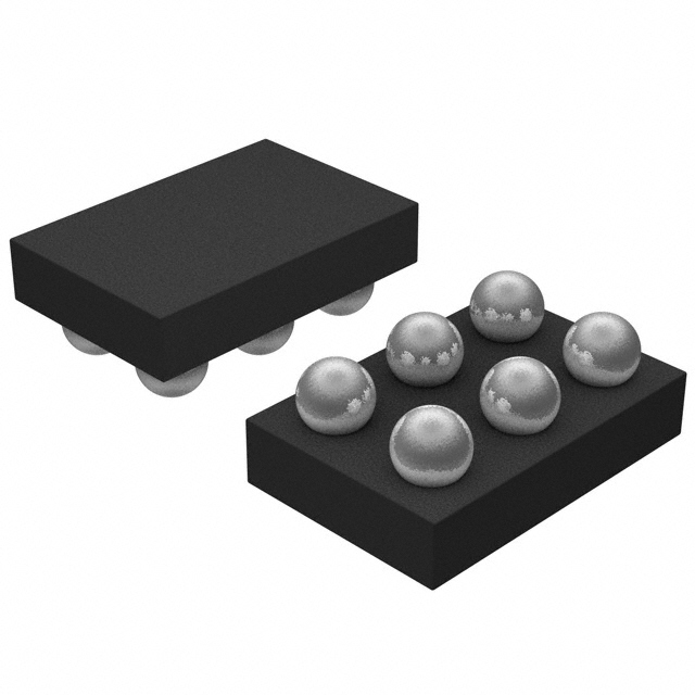
WLCSP6, 1.2x0.8
CASE 567MV
XXMG
XX = Specific Device Code
M = Month Code
G
= Pb−Free Package
• High Current Bias Rail Topology for OUT1
• High PSRR, Ultra Low Noise LDO for OUT2
• Output voltage range: OUT1 – 0.8 V to 1.8 V
•
•
www.onsemi.com
(Factory trimmed) OUT2 – 1.8 V to 3.6 V
Low IQ of typ. 90 mA
Slow VOUT Slew Rate for Camera Modules (Optional)
typ. ≤30 mV/ms
Ultra−Low Dropout: OUT1 typ. 70 mV @ 1.2 V/500 mA
Ultra−Low Dropout: OUT2 typ. 95 mV @ 2.8 V/250 mA
±1% Typical Accuracy
High PSRR: OUT1 typ. 70 dB at 1 kHz
High PSRR: OUT2 typ. 92 dB at 1 kHz
Thermal Shutdown and Current Limit Protections
Stable with a Small Ceramic Capacitor
Available WLCSP−6 1.2x0.8 mm Package
Active Output Discharge for Fast Output Turn−Off
These are Pb−free Devices
PIN CONNECTIONS
1
2
A
IN1
OUT1
B
EN
GND
C
IN2
OUT2
(Top View)
ORDERING INFORMATION
See detailed ordering, marking and shipping information on
page 8 of this data sheet.
Typical Applications
• Camera Modules
• Smartphones, Tablets
NCP 156
V IN1
V IN2
C IN1
1 mF
C IN2
IN1
OUT1
IN2
OUT2
EN
GND
1 mF
V OUT1
V OUT2
C OUT2
C OUT1
1 mF
2.2 mF
Figure 1. Typical Application Schematic
© Semiconductor Components Industries, LLC, 2017
September, 2019 − Rev. 1
1
Publication Order Number:
NCP156/D
�NCP156
OUT1
IN1
MOSFET
DRIVER WITH
CURRENT
LIMIT
THERMAL
SHUTDOWN
*Active
discharge
(A option only)
ENABLE
LOGIC
EN
OUTPUT
VOLTAGE
TRIMMING
BANDGAP
REFERENCE
THERMAL
SHUTDOWN
GND
MOSFET
DRIVER WITH
CURRENT
LIMIT
IN2
OUT2
Figure 2. Simplified Schematic Block Diagram
Table 1. PIN FUNCTION DESCRIPTION
Pin No.
Pin Name
A1
IN1
A2
OUT1
B1
EN
B2
GND
C1
IN2
C2
OUT2
Description
Output 1 – Power Supply pin
Regulated Output 1 Voltage pin
Applying VEN < 0.4 V disables the regulator; Pulling VEN > 0.9 V enables both voltage outputs.
Common ground connection
Output 2 – Power Supply pin, Output 1 – Control Supply pin
Regulated Output 2 Voltage pin
Table 2. THERMAL CHARACTERISTICS (Note 1)
Rating
Symbol
Thermal Characteristics, WLCSP6 1.2x0.8mm,
Thermal Resistance, Junction−to−Air
qJA
Value
90
Unit
°C/W
1. Single component mounted on 1 oz, FR4 PCB with 645mm2 Cu area
Table 3. ABSOLUTE MAXIMUM RATINGS
Symbol
Value
Unit
Input Voltage 1 (Note 2)
Rating
VIN1
−0.3 to 6
V
Input Voltage 2 (Note 2)
VIN2
−0.3 to 6
V
Output Voltage 1
VOUT1
−0.3 to VIN1 + 0.3
V
Output Voltage 2
VOUT2
−0.3 to VIN2 + 0.3
V
Enable Input
VEN
−0.3 to 6
V
Output Short Circuit Duration
tSC
Indefinite
s
TJ(MAX)
150
°C
TSTG
−55 to 125
°C
ESDHBM
2000
V
Maximum Junction Temperature
Storage Temperature
ESD Capability, Human Body Model (Note 3)
ESD Capability, Machine Model (Note 3)
ESDMM
200
V
ESD Capability, Charged Device Model (Note 3)
ESDCDM
1000
V
Stresses exceeding those listed in the Maximum Ratings table may damage the device. If any of these limits are exceeded, device functionality
should not be assumed, damage may occur and reliability may be affected.
2. Refer to ELECTRICAL CHARACTERISTICS and APPLICATION INFORMATION for Safe Operating Area.
3. This device series incorporates ESD protection and is tested by the following methods:
ESD Human Body Model tested per AEC−Q100−002 (EIA/JESD22−A114)
ESD Machine Model tested per AEC−Q100−003 (EIA/JESD22−A115)
ESD Charged Device Model tested per EIA/JESD22−C101, Field Induced Charge Model
Latchup Current Maximum Rating tested per JEDEC standard: JESD78.
www.onsemi.com
2
�NCP156
Table 4. ELECTRICAL CHARACTERISTICS −40°C ≤ TJ ≤ 125°C; VIN1 = VOUT1(NOM) +0.3 V, VIN2 = 2.7 V or (VOUT1 + 1.6 V) or
VOUT2(NOM) + 0.3 V whichever is greater, IOUT1 = IOUT2 = 1 mA, VEN = 1 V, unless otherwise noted. CIN1 = CIN2 = 1 mF, COUT1 = 2.2 mF,
COUT2 = 1 mF. Typical values are at TJ = +25°C. Min/Max values are for −40°C ≤ TJ ≤ 125°C unless otherwise noted.
Parameter
Test Conditions
Operating Input Voltage
Range
Output Voltage Accuracy
TJ = 25°C
Undervoltage Lock−out
VIN2 Rising
Symbol
Min
Max
Unit
VIN1
VOUT1 +
VDO
5.5
V
VIN2
VIN2 =
(VOUT1+1.
5) ≥ 2.4 or
VOUT2(NO
M)+VDO,
whichever
is greater
5.5
VOUT1
Typ
±1
%
1.5
V
VOUT2
UVLO
Hysteresis
Output Voltage Accuracy
0.2
VOUT1(NOM) + 0.3 V ≤ VIN1
≤ VOUT1(NOM) + 1.0 V,
VOUT2 = 2.7 V or
(VOUT1(NOM)) + 1.6 V),
whichever is greater, 1 mA
< IOUT1 < 500 mA
VOUT1 < 1.2 V
VOUT1 ≥ 1.2 V
VIN2 = (VOUT2(NOM) + 0.3 V) to 5.5 V,
0 mA ≤ IOUT2 ≤ 250 mA
Line Regulation
Load Regulation
Dropout Voltage
(Note 5)
VOUT2
−18
+18
mV
−1.5
+1.5
%
−2
+2
%
LineREG
VOUT1
VOUT1(NOM) + 0.3 V ≤ VIN1 ≤ 5.5 V
VOUT2
VOUT2(NOM) + 0.3 V ≤ VIN2 ≤ 5.5 V
0.02
VIN2 to
VOUT1
(2.7 V or (VOUT1(NOM) + 1.6 V), whichever is greater) < VIN2 < 5.5 V
0.01
OUT1
IOUT1 = 1 mA to 500 mA
OUT2
IOUT2 = 1 mA to 250 mA
OUT1
IOUT1 = 500 mA
OUT2
IOUT2 = 250 mA
OUT1
%/V
0.01
LoadREG
mV
5
1
VDO
VOUT2(NOM) = 2.8 V
VIN2 to VOUT1 Dropout Voltage IOUT1 = 500 mA, VIN1 = VIN2 (Notes 5, 6)
Output Current Limit
VOUT1
VOUT = 90% VOUT(NOM)
VDO(IN2)
ICL
OUT2
70
150
95
160
1.1
1.5
550
850
300
550
IOUT1 = 0 mA
IQ1
10
20
Quiescent Current IN2
IOUT2 = 0 mA
IQ2
80
130
Disable Current
VIN1 Pin
IIN1(DIS)
0.05
1
0.1
1
EN Pin Threshold Voltage
VIN2 Pin
IIN2(DIS)
EN Input Voltage “H”
VEN(H)
EN Input Voltage “L”
VEN(L)
EN Pull Down Current
VEN = 5.5 V
Turn−On Delay
OUT1
From assertion of VEN to raising VOUT
OUT2
V
mA
Quiescent Current IN1
VEN1 ≤ 0.4 V
mV
mA
mA
V
0.9
0.4
IEN
0.3
tDELAY
200
2
mA
ms
130
Product parametric performance is indicated in the Electrical Characteristics for the listed test conditions, unless otherwise noted. Product
performance may not be indicated by the Electrical Characteristics if operated under different conditions.
4. Performance guaranteed over the indicated operating temperature range by design and/or characterization. Production tested at TA =
25°C. Low duty cycle pulse techniques are used during the testing to maintain the junction temperature as close to ambient as possible.
5. Dropout voltage is characterized when VOUT falls 3% below VOUT(NOM).
6. For output 1 voltages below 0.9 V, VIN2 to VOUT1 dropout voltage does not apply due to a minimum VIN2 operating voltage of 2.4 V.
7. Refer to Table 6 for output slew rate configuration.
www.onsemi.com
3
�NCP156
Table 4. ELECTRICAL CHARACTERISTICS −40°C ≤ TJ ≤ 125°C; VIN1 = VOUT1(NOM) +0.3 V, VIN2 = 2.7 V or (VOUT1 + 1.6 V) or
VOUT2(NOM) + 0.3 V whichever is greater, IOUT1 = IOUT2 = 1 mA, VEN = 1 V, unless otherwise noted. CIN1 = CIN2 = 1 mF, COUT1 = 2.2 mF,
COUT2 = 1 mF. Typical values are at TJ = +25°C. Min/Max values are for −40°C ≤ TJ ≤ 125°C unless otherwise noted.
Parameter
VOUT Slew Rate (Note 7)
Test Conditions
Symbol
Normal
VOUT2
200
VOUT1
15
VOUT2
30
PSRR(VIN1)
70
VIN2 to VOUT2, f = 1 kHz, IOUT2 = 10 mA, VIN2 ≥
VOUT +0.5 V
PSRR(VIN2)
92
VIN2 to VOUT1, f = 1 kHz, IOUT1 = 150 mA, VIN1 ≥
VOUT1 +0.5 V
PSRR(IN2 to
80
Power Supply Rejection Ratio VIN1 to VOUT1, f = 1 kHz, IOUT1 = 150 mA, VIN1 ≥
VOUT +0.5 V
OUT1
OUT2
VIN = VOUT +0.5 V
f = 10 Hz to 100 kHz
Max
Unit
mV/ms
dB
OUT1)
VN
40
mVRMS
8.5
Thermal Shutdown Threshold Temperature increasing
Temperature decreasing
Output Discharge Pull−Down
Typ
100
Slow
Output Noise Voltage
Min
VOUT1
VEN ≤ 0.4 V
(only if Active Discharge feature enabled)
TSDL
160
TSDH
140
RDISCH
150
°C
W
Product parametric performance is indicated in the Electrical Characteristics for the listed test conditions, unless otherwise noted. Product
performance may not be indicated by the Electrical Characteristics if operated under different conditions.
4. Performance guaranteed over the indicated operating temperature range by design and/or characterization. Production tested at TA =
25°C. Low duty cycle pulse techniques are used during the testing to maintain the junction temperature as close to ambient as possible.
5. Dropout voltage is characterized when VOUT falls 3% below VOUT(NOM).
6. For output 1 voltages below 0.9 V, VIN2 to VOUT1 dropout voltage does not apply due to a minimum VIN2 operating voltage of 2.4 V.
7. Refer to Table 6 for output slew rate configuration.
www.onsemi.com
4
�NCP156
TYPICAL CHARACTERISTICS
2.808
VOUT1, OUTPUT VOLTAGE (V)
1.204
VOUT2, OUTPUT VOLTAGE (V)
1.206
IOUT = 1 mA
1.202
1.200
1.198
IOUT = 500 mA
1.196
1.194
1.192
1.190
0
20
40
60
80
100
120
140
2.804
2.802
IOUT = 1 mA
2.800
IOUT = 250 mA
2.798
VIN1 = 1.5 V
VIN2 = 3.1 V
VOUT1 = 1.2 V
VOUT2 = 2.8 V
COUT1 = 2.2 mF (MLCC)
COUT2 = 1 mF (MLCC)
2.796
2.794
2.792
2.790
2.788
−40 −20
0
20
40
60
80
100
120 140
TJ, JUNCTION TEMPERATURE (°C)
TJ, JUNCTION TEMPERATURE (°C)
Figure 3. Output Voltage vs. Temperature −
VOUT1 = 1.2 V
Figure 4. Output Voltage vs. Temperature −
VOUT2 = 2.8 V
3.0
2.5
2.0
1.5
1.0
0.5
0
REGLINE, LINE REGULATION (mV)
VIN1 = 1.5 V to 5.5 V
VIN2 = 3.1 V
VOUT1 = 1.2 V
VOUT2 = 2.8 V
IOUT1 = IOUT2 = 1 mA
COUT1 = 2.2 mF (MLCC)
COUT2 = 1 mF (MLCC)
−0.5
−1.0
−1.5
−2.0
−2.5
−3.0
−40 −20
0
20
40
60
80
100
120
140
3.0
2.5
2.0
1.5
1.0
0.5
VIN1 = 1.5 V
VIN2 = 3.1 V to 5.5 V
VOUT1 = 1.2 V
VOUT2 = 2.8 V
IOUT1 = IOUT2 = 1 mA
COUT1 = 2.2 mF (MLCC)
COUT2 = 1 mF (MLCC)
0
−0.5
−1.0
−1.5
−2.0
−2.5
−3.0
−40 −20
0
20
40
60
80
100
120 140
TJ, JUNCTION TEMPERATURE (°C)
TJ, JUNCTION TEMPERATURE (°C)
Figure 5. Line Regulation vs. Temperature −
VOUT1 = 1.2 V
Figure 6. Line Regulation vs. Temperature −
VOUT = 2.8 V
10
REGLOAD, LOAD REGULATION (mV)
REGLOAD, LOAD REGULATION (mV)
REGLINE, LINE REGULATION (mV)
1.188
1.186
−40 −20
VIN1 = 1.5 V
VIN2 = 3.1 V
VOUT1 = 1.2 V
VOUT2 = 2.8 V
COUT1 = 2.2 mF (MLCC)
COUT2 = 1 mF (MLCC)
2.806
9
8
7
6
VIN1 = 1.5 V
VIN2 = 3.1 V
VOUT1 = 1.2 V
VOUT2 = 2.8 V
IOUT1 = 1 mA to 500 mA
IOUT2 = 1 mA
COUT1 = 2.2 mF (MLCC)
COUT2 = 1 mF (MLCC)
5
4
3
2
1
0
−40 −20
0
20
40
60
80
100
120
140
5.0
4.5
4.0
3.5
3.0
2.5
2.0
VIN1 = 1.5 V
VIN2 = 3.1 V
VOUT1 = 1.2 V
VOUT2 = 2.8 V
IOUT1 = 1 mA
IOUT2 = 1 mA to 250 mA
COUT1 = 2.2 mF (MLCC)
COUT2 = 1 mF (MLCC)
1.5
1.0
0.5
0
−40 −20
0
20
40
60
80
100
120 140
TJ, JUNCTION TEMPERATURE (°C)
TJ, JUNCTION TEMPERATURE (°C)
Figure 7. Load Regulation vs. Temperature −
VOUT1 = 1.2 V
Figure 8. Load Regulation vs. Temperature −
VOUT = 2.8 V
www.onsemi.com
5
�NCP156
APPLICATIONS INFORMATION
General
VOUT1_NOM + 0.3 V. The input voltage 2 is used as bias
voltage of N−MOS output together with supply OUT2 and
must be chosen more carefully. The basic condition to VIN2
selections is the same as for first input VIN2 ≥ VOUT2_NOM
+ VDO2. Due to the fact that VIN2 is also bias voltage for
N−MOS regulator difference between VOUT1 and VIN2
must be at least 1.5 V.
The internal voltage references for both channels have
cascade topology. It means reference VREF2 for OUT2 is
derived from IN2 and reference for OUT1 is derived also
from reference VREF2 not from VIN1. All negative effects on
VREF2 is visible also on VREF1 and then on VOUT1. The
reference voltage VREF2 has same value as VOUT2 due to
there is necessary to have enough voltage headroom
between VIN2 and VOUT2. If VOUT2 is in dropout region then
OUT1 is affected too. Consequently the OUT1 output
voltage is lower than nominal due to lower VREF1 reference
which is affected by drop VREF2. For more information
please refer design note DN05110/D.
The NCP156 is a 500 mA/250 mA dual output high
performance Low Dropout Linear Regulator. It offers
unique combination of N−MOS and P−MOS regulators to
provide the best performance and power efficiency. The
device is optimized for camera sensor applications to supply
digital and analog power rails. Digital supply rail requires
high current, low input voltage and as low as possible
dropout to achieve the best efficiency and analog pixel array
requires less current but very stable and clean supply line
with very fast transient response. The NCP156 is offered in
WLCSP6 package which helps with high integration as
close as possible to sensor for best parameters.
Input Capacitor Selection (CIN)
It is recommended to connect at least a 1 mF Ceramic X5R
or X7R capacitor as close as possible to the IN pin of the
device. Larger input capacitor may be necessary if fast and
large load transients are encountered in the application. This
capacitor will provide a low impedance path for unwanted
AC signals or noise modulated onto constant input voltage.
There is no requirement for the min. or max. ESR of the input
capacitor but it is recommended to use ceramic capacitors
for their low ESR and ESL. A good input capacitor will limit
the influence of input trace inductance and source resistance
during sudden load current changes.
Enable Operation
The NCP156 uses the single EN pin for both output
channels. If the EN pin voltage is 0.9 V the device is guaranteed to
be enabled. The NCP156 regulates the output voltage and
the active discharge transistor is turned−off.
The EN pin has internal pull−down current source with
typ. value of 300 nA which assures that the device is
turned−off when the EN pin is not connected. In the case
where the EN function isn’t required the EN should be tied
directly to IN.
Output Decoupling (COUT)
The NCP156 requires an output capacitor for each output
connected as close as possible to the output pin of the
regulator. The recommended capacitor value for OUT1 is
2.2 mF and X7R or X5R dielectric due to its low capacitance
variations over the specified temperature range.
Recommended output capacitor for OUT2 is 1 mF same type
as OUT1. The NCP156 is designed to remain stable with
minimum effective capacitance of 1 mF for OUT1 and
0.7 mF for OUT2 to account for changes with temperature,
DC bias and package size. Especially for small package size
capacitors such as 0201 the effective capacitance drops
rapidly with the applied DC bias.
There is no requirement for the minimum value of
Equivalent Series Resistance (ESR) for the COUT but the
maximum value of ESR should be less than 1.9 W. Larger
output capacitors and lower ESR could improve the load
transient response or high frequency PSRR. It is not
recommended to use tantalum or electrolytic capacitors on
the output due to their large ESR. They can be used in
connection with appropriate ceramic capacitor as secondary
energy reservoir.
Slew Rate Control
The NCP156 is optimized for camera sensor application
and meets all requirements for using in modern camera
applications such as a smartphones, cameras and image
capture devices. Power supply specification of sensors often
requires output voltage slew rate limitation to protect sensor
during regulator start−up. The NCP156 incorporates
soft−start feature which can assure safe start−up output
voltage ramp without excess current spikes and voltage
undershoots. The device provides two options of slew rate
speed, normal means typical slew rate about 100/200 mV/ms
(OUT1/OUT2) and slow option means VIN.
Due to this fact in cases, where the extended reverse current
condition can be anticipated the device may require
additional external protection.
The NCP156 device offers various combinations of active
discharge feature and VOUT slew rate speed for each output
channel. The OPN contains two letters behind product name
which are dedicated for Active discharge and Slew rate
speed. Possible combinations with corresponding letters are
explained below.
Power Supply Rejection Ratio
The NCP156 features very good Power Supply Rejection
ratio. If desired the PSRR at higher frequencies in the range
100 kHz – 10 MHz can be tuned by the selection of COUT
capacitor and proper PCB layout.
Table 5. ACTIVE DISCHARGE OPTION
Act. Discharge (x = ON)
OUT1
OUT2
A
x
x
B
PCB Layout Recommendations
C
To obtain good transient performance and good regulation
characteristics place input and output capacitors close to the
device pins and make the PCB traces wide. In order to
minimize the solution size, use 0402 capacitors. Larger
copper area connected to the pins will also improve the
device thermal resistance. The actual power dissipation can
be calculated from the equation above (Equation 2). Expose
pad should be tied the shortest path to the GND pin.
x
D
x
Table 6. VOUT SLEW RATE SPEED
Slew rate (x = Slower)
OUT1
OUT2
A
x
x
B
C
x
D
x
ORDERING INFORMATION
Device
Marking
Voltage Option
OUT1 / OUT2
Active Discharge
OUT1 / OUT2
VOUT Slew Rate
OUT1 / OUT2
NCP156AAFCT100280T2G*
DL
1.0 V / 2.8 V
Yes / Yes
Slow / Slow
NCP156AAFCT105280T2G
DM
1.05 V / 2.8 V
Yes / Yes
Slow / Slow
NCP156AAFCT110280T2G*
DN
1.1 V / 2.8 V
Yes / Yes
Slow / Slow
NCP156AAFCT120180T2G*
DA
1.2 V / 1.8 V
Yes / Yes
Slow / Slow
NCP156AAFCT120270T2G*
DP
1.2 V / 2.7 V
Yes / Yes
Slow / Slow
NCP156AAFCT120280T2G
DR
1.2 V / 2.8 V
Yes / Yes
Slow / Slow
NCP156ABFCT100280T2G
DD
1.0 V / 2.8 V
Yes / Yes
Normal / Normal
NCP156ABFCT105280T2G*
DK
1.05 V / 2.8 V
Yes / Yes
Normal / Normal
NCP156ABFCT110280T2G
DE
1.1 V / 2.8 V
Yes / Yes
Normal / Normal
NCP156ABFCT120270T2G*
DG
1.2 V / 2.7 V
Yes / Yes
Normal / Normal
NCP156ABFCT120280T2G
DF
1.2 V / 2.8 V
Yes / Yes
Normal / Normal
NCP156ABFCT180250T2G*
DJ
1.8 V / 2.5 V
Yes / Yes
Normal / Normal
NCP156ABFCT180270T2G*
DH
1.8 V / 2.7 V
Yes / Yes
Normal / Normal
NCP156BBFCT120180T2G*
DC
1.2 V / 1.8 V
No / No
Normal / Normal
Package
Shipping†
WLCSP6
(Pb−Free)
5000 /
Tape &
Reel
†For information on tape and reel specifications, including part orientation and tape sizes, please refer to our Tape and Reel Packaging
Specifications Brochure, BRD8011/D.
*Please contact local sales representative for availability.
www.onsemi.com
8
�MECHANICAL CASE OUTLINE
PACKAGE DIMENSIONS
WLCSP6, 1.20x0.80
CASE 567MV
ISSUE B
SCALE 4:1
DATE 05 JUN 2018
E
A
È
PIN A1
REFERENCE
B
NOTES:
1. DIMENSIONING AND TOLERANCING PER
ASME Y14.5M, 1994.
2. CONTROLLING DIMENSION: MILLIMETERS.
3. COPLANARITY APPLIES TO SPHERICAL
CROWNS OF SOLDER BALLS.
D
0.05 C
2X
DIM
A
A1
A2
b
D
E
e
0.05 C
2X
TOP VIEW
A2
A
0.05 C
0.05 C
A1
NOTE 3
6X
GENERIC
MARKING DIAGRAM*
SIDE VIEW
b
0.05 C A B
MILLIMETERS
MIN
MAX
0.33
−−−
0.04
0.08
0.23 REF
0.24
0.30
1.20 BSC
0.80 BSC
0.40 BSC
C
SEATING
PLANE
e
e
C
XXM
XX = Specific Device Code
M = Month Code
*This information is generic. Please refer to
device data sheet for actual part marking.
Pb−Free indicator, “G” or microdot “ G”,
may or may not be present.
0.03 C
B
A
1
2
BOTTOM VIEW
RECOMMENDED
SOLDERING FOOTPRINT*
A1
0.40
PITCH
0.40
PITCH
PACKAGE
OUTLINE
6X
0.20
DIMENSIONS: MILLIMETERS
*For additional information on our Pb−Free strategy and soldering
details, please download the ON Semiconductor Soldering and
Mounting Techniques Reference Manual, SOLDERRM/D.
DOCUMENT NUMBER:
DESCRIPTION:
98AON06670G
WLCSP6, 1.20x0.80
Electronic versions are uncontrolled except when accessed directly from the Document Repository.
Printed versions are uncontrolled except when stamped “CONTROLLED COPY” in red.
PAGE 1 OF 1
ON Semiconductor and
are trademarks of Semiconductor Components Industries, LLC dba ON Semiconductor or its subsidiaries in the United States and/or other countries.
ON Semiconductor reserves the right to make changes without further notice to any products herein. ON Semiconductor makes no warranty, representation or guarantee regarding
the suitability of its products for any particular purpose, nor does ON Semiconductor assume any liability arising out of the application or use of any product or circuit, and specifically
disclaims any and all liability, including without limitation special, consequential or incidental damages. ON Semiconductor does not convey any license under its patent rights nor the
rights of others.
© Semiconductor Components Industries, LLC, 2018
www.onsemi.com
�onsemi,
, and other names, marks, and brands are registered and/or common law trademarks of Semiconductor Components Industries, LLC dba “onsemi” or its affiliates
and/or subsidiaries in the United States and/or other countries. onsemi owns the rights to a number of patents, trademarks, copyrights, trade secrets, and other intellectual property.
A listing of onsemi’s product/patent coverage may be accessed at www.onsemi.com/site/pdf/Patent−Marking.pdf. onsemi reserves the right to make changes at any time to any
products or information herein, without notice. The information herein is provided “as−is” and onsemi makes no warranty, representation or guarantee regarding the accuracy of the
information, product features, availability, functionality, or suitability of its products for any particular purpose, nor does onsemi assume any liability arising out of the application or use
of any product or circuit, and specifically disclaims any and all liability, including without limitation special, consequential or incidental damages. Buyer is responsible for its products
and applications using onsemi products, including compliance with all laws, regulations and safety requirements or standards, regardless of any support or applications information
provided by onsemi. “Typical” parameters which may be provided in onsemi data sheets and/or specifications can and do vary in different applications and actual performance may
vary over time. All operating parameters, including “Typicals” must be validated for each customer application by customer’s technical experts. onsemi does not convey any license
under any of its intellectual property rights nor the rights of others. onsemi products are not designed, intended, or authorized for use as a critical component in life support systems
or any FDA Class 3 medical devices or medical devices with a same or similar classification in a foreign jurisdiction or any devices intended for implantation in the human body. Should
Buyer purchase or use onsemi products for any such unintended or unauthorized application, Buyer shall indemnify and hold onsemi and its officers, employees, subsidiaries, affiliates,
and distributors harmless against all claims, costs, damages, and expenses, and reasonable attorney fees arising out of, directly or indirectly, any claim of personal injury or death
associated with such unintended or unauthorized use, even if such claim alleges that onsemi was negligent regarding the design or manufacture of the part. onsemi is an Equal
Opportunity/Affirmative Action Employer. This literature is subject to all applicable copyright laws and is not for resale in any manner.
PUBLICATION ORDERING INFORMATION
LITERATURE FULFILLMENT:
Email Requests to: orderlit@onsemi.com
onsemi Website: www.onsemi.com
◊
TECHNICAL SUPPORT
North American Technical Support:
Voice Mail: 1 800−282−9855 Toll Free USA/Canada
Phone: 011 421 33 790 2910
Europe, Middle East and Africa Technical Support:
Phone: 00421 33 790 2910
For additional information, please contact your local Sales Representative
�


 工商网监
湘ICP备2023018690号
工商网监
湘ICP备2023018690号
