NCP1589D
Low Voltage Synchronous
Buck Controller with Light
Load Efficiency and
Transient Enhancement
The NCP1589D is a low cost PWM controller designed to operate
from a 5 V or 12 V supply. This device is capable of producing an
output voltage as low as 0.8 V and converting voltage from as low as
2.5 V. It is easy to operate and provides an optimal level of integration
to reduce size and cost of the power supply. It operates in Ramp Pulse
Modulation mode for superior load step and release response. In
addition to fast transient response, it also includes a 1.5 A gate driver
design and light load efficiency features such as adaptive non−overlap
circuitry and diode emulation. It normally operates at a range of
200−500 kHz in continuous current conduction mode, which reduces
with current at light load for further power saving. Protection features
include programmable overcurrent protection, output overvoltage and
undervoltage protection and input undervoltage lockout (UVLO).
VCC Range from 4.5 V to 13.2 V
Adjustable Operating frequency
Boost Pin Operates to 35 V
Ramp Pulse Modulation Control
Precision 0.8 V Internal Reference
Adjustable Output Voltage
Internal 1.5 A Gate Drivers
80% Max Duty Cycle
Input Under Voltage Lockout
Programmable Current Limit
Adaptive Diode Mode Emulation in Light Load
This is a Pb−Free Device
January, 2017 − Rev. 2
1589D
A
L
Y
W
G
= Specific Device Code
= Assembly Location
= Wafer Lot
= Year
= Work Week
= Pb−Free Device
BOOT
1
10
PGOOD
LX
2
9
VORPM
UG
3
8
FB
LG
4
GND
5
Flag
7
COMP/DISB
6
VCC
(Top View)
ORDERING INFORMATION
Graphics Cards
Desktop Computers
Servers / Networking
DSP & FPGA Power Supply
DC−DC Regulator Modules
© Semiconductor Components Industries, LLC, 2017
1589D
ALYWG
G
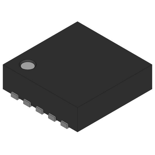
DFN10
CASE 485C
PIN CONNECTIONS
Applications
•
•
•
•
•
MARKING
DIAGRAM
(Note: Microdot may be in either location)
Features
•
•
•
•
•
•
•
•
•
•
•
•
www.onsemi.com
Device
Package
Shipping†
NCP1589DMNTWG
DFN10
(Pb−Free)
3000 /
Tape & Reel
†For information on tape and reel specifications,
including part orientation and tape sizes, please
refer to our Tape and Reel Packaging Specifications
Brochure, BRD8011/D.
1
Publication Order Number:
NCP1589D/D
�NCP1589D
VCC = 4.5 V − 13.2 V
VBST = 4.5 V − 15 V
VIN = 2.5 V − 19 V
VCC
PGOOD
BOOT
COMP/DISB
UG
R2
VOUT
LX
C2
FB
LG
FLAG
ROCSET
C1
GND VORPM
C3
R4
R1
R3
R9
R10
GND
Figure 1. Typical Application Diagram
PGOOD
PGOOD
MONITOR
OV and UV
VORPM 9
±10% of Vref
±25% of Vref
0.8 V
(Vref)
POR
UVLO
8
−
6
VCC
1
BOOT
3
UG
2
LX
4
LG
5
GND
VOCP
−
FAULT
−
+
+
LATCH
FAULT
FB
10
R
+
0.8 V
(Vref)
S
PWM
OUT
Q
+
−
RPMSET
2V
+
RAMP
LX
−
COMP VPRM
VORPM
COMP/DISB
7
FAULT
LX
Figure 2. Detailed Block Diagram
www.onsemi.com
2
AZCD logic
VCC
�NCP1589D
PIN FUNCTION DESCRIPTION
Pin No.
Symbol
1
BOOT
Description
2
LX
Switch node pin. This is the reference for the floating top gate driver. Connect this pin to the source of the
top MOSFET. Also used for low side MOSFET RDS(on) current detection and diode emulation.
3
UG
Top gate MOSFET driver pin. Connect this pin to the gate of the top N−channel MOSFET.
4
LG
Bottom gate MOSFET driver pin. Connect this pin to the gate of the bottom N−channel MOSFET. Also used
to set the overcurrent limit.
5
GND
IC ground reference. All control circuits are referenced to this pin. Connect to FLAG.
6
VCC
Supply rail for the internal circuitry. Operating supply range is 4.5 V to 13.2 V. Decouple with a 1 mF capacitor to GND. Ensure that this decoupling capacitor is placed near the IC. Also low−side MOSFET drive voltage.
7
COMP/DISB
8
FB
9
VORPM
Output voltage information for RPM threshold
10
PGOOD
Power Good output. Pulled Low if VFB is outside ±10% of 0.8 V Vref.
Supply rail for the floating top gate driver. To form a boost circuit, use an external diode to bring the desired
input voltage to this pin (cathode connected to BOOT pin). Connect a capacitor (CBOOT) between this pin
and the LX pin. Typical values for CBOOT range from 0.1 mF to 1 mF. Ensure that CBOOT is placed near the
IC.
Compensation Pin. This is the output of the error amplifier (EA) and the non−inverting input of the PWM
comparator. Use this pin in conjunction with the FB pin to compensate the voltage−control feedback loop.
Pull this pin low for disable.
This pin is the inverting input to the error amplifier. Use this pin in conjunction with the COMP pin to compensate the voltage−control feedback loop. Connect this pin to the output resistor divider (if used) or directly
to Vout.
ABSOLUTE MAXIMUM RATINGS
Pin Name
Symbol
VMAX
VMIN
VCC
15 V
−0.3 V
BOOT
35 V wrt/GND
40 V < 100 ns
15 V wrt/LX
−0.3 V
−0.3 V
−0.3 V
Switching Node (Bootstrap Supply Return)
LX
35 V
40 V for < 100 ns
−5 V
−10 V for < 200 ns
High−Side Driver Output (Top Gate)
UG
30 V wrt/GND
15 V wrt/LX
40 V for < 100 ns
−0.3 V wrt/LX
−5 V for < 200 ns
Low−Side Driver Output (Bottom Gate)
LG
15 V
−0.3 V
−5 V for < 200 ns
Feedback, VORPM
FB, VORPM
6.0 V
−0.3 V
COMP/DISB
COMP/DISB
5.5 V
−0.3 V
PGOOD
7V
−0.3 V
Symbol
Value
Unit
Thermal Resistance, Junction−to−Ambient
RqJA
165
°C/W
Thermal Resistance, Junction−to−Case
RqJC
45
°C/W
Operating Junction Temperature Range
TJ
0 to 150
°C
Main Supply Voltage Input
Bootstrap Supply Voltage Input
PGOOD
MAXIMUM RATINGS
Rating
Operating Ambient Temperature Range
TA
0 to 95
°C
Storage Temperature Range
Tstg
−55 to +150
°C
Moisture Sensitivity Level
MSL
1
−
Stresses exceeding those listed in the Maximum Ratings table may damage the device. If any of these limits are exceeded, device functionality
should not be assumed, damage may occur and reliability may be affected.
www.onsemi.com
3
�NCP1589D
ELECTRICAL CHARACTERISTICS (0°C < TA < 95°C; 4.5 V < [BOOT−LX] < 13.2 V, 4.5 V < BOOT < 30 V, 0 V < LX < 21 V,
CTG = CBG = 1.0 nF, for min/max values unless otherwise noted.)
Characteristic
Conditions
VCC Input Voltage Range
BOOT Voltage Range
13.2 V wrt LX
dV/dt on VCC
Min
Typ
Max
Unit
4.5
13.2
V
4.5
30
V
−10
10
V/ms
1.0
%
3.8
mA
100
mA
VREF AND ERROR AMPLIFIER
Vref
Reference Voltage
Output Voltage Accuracy
Reference and Error Amplifier Excluding
External Resistive Divider Tolerance
0.8
−1.0
V
SUPPLY CURRENT
VCC Quiescent Supply Current
No Switching, VCC = 13.2 V
BOOT Quiescent Current
No Switching
2.5
0.1
UNDERVOLTAGE LOCKOUT
VCC UVLO Threshold
VCC Rising
4.4
V
VCC UVLO Threshold
VCC Falling
4.0
V
VCC UVLO Hysteresis
VCC Rising or VCC Falling
400
mV
Ramp Slope
0.5
V/ms
Ramp−Amplitude Voltage
1.50
V
0
%
SWITCHING REGULATOR
Minimum Duty Cycle
Maximum Duty Cycle
70
LG Minimum on Time
200
83
92
%
350
ns
ERROR AMPLIFIER
80
Open Loop DC Gain (Note 1)
Output Source Current
Output Sink Current
Vfb < 0.8 V
Vfb > 0.8 V
120
dB
2.0
2.0
mA
Unity Gain Bandwidth (Note 1)
15
MHz
Disable Threshold
0.7
Output Source Current During Disable
0.8
0.9
V
10
40
mA
GATE DRIVERS
Upper Gate Source
BOOT − LX = 5 V
Upper Gate Sink
BOOT − LX = 5 V
1.5
A
1.8
W
VCC = 5 V
1.2
W
UG Falling to LG Rising Delay Tdead1
(Note 1)
VCC = 12 V, UG−LX < 1.0 V, LG > 1.0 V
Only Valid for CCM Operating Mode
20
30
ns
LG Falling to UG Rising Delay Tdead2
(Note 1)
VCC = 12 V, LG < 1.0 V, UG > 1.0 V
Only Valid for CCM Operating Mode
20
30
ns
Unbiased, BOOT − LX = 0
45
kW
45
kW
Lower Gate Source
VCC = 5 V
Lower Gate Sink
UG Internal Resistor to LX
LX Internal Resistor to GND
1.5
A
SOFT−START
Soft−Start Time
Enable to Soft−Start Delay (Note 1)
VCC > 4.5 V, COMP w Disable Threshold
VCC > 4.5 V, COMP Rises and Crosses
Disable Threshold
1. Guaranteed by design but not tested in production.
www.onsemi.com
4
2.0
2.6
ms
500
ms
�NCP1589D
ELECTRICAL CHARACTERISTICS (0°C < TA < 95°C; 4.5 V < [BOOT−LX] < 13.2 V, 4.5 V < BOOT < 30 V, 0 V < LX < 21 V,
CTG = CBG = 1.0 nF, for min/max values unless otherwise noted.)
Characteristic
Conditions
Min
Typ
Max
Unit
0.4
V
880
902
mV
POWER GOOD INCLUDING OVP AND UVP THRESHOLD
Logic Low, Sinking 4 mA
Output Voltage
Overvoltage until PGOOD goes low
Undervoltage until PGOOD goes low
698
720
mV
PGOOD High Upper Limit Hysteresis
16
mV
PGOOD High Lower Limit Hysteresis
16
mV
OVP Threshold to Part Disable
950
1000
1030
mV
UVP Threshold to Part Disable
570
600
630
mV
1.0
ms
350
ns
40
ns
Power Good Delay (Note 1)
ZERO CURRENT DETECTION (LX Pin)
LX > 50 mV, LG on time
Zero Current Detection Blank Timer after
TG < 1.0 V
Capture Time for LX Voltage (Note 1)
200
250
Time to Capture LX Voltage Once LG is <
1.0 V
ZERO CURRENT Vth ADJUSTMENT DETECTION (LX Pin)
Negative LX Detection Voltage
Vbdls
200
300
400
mV
Positive LX Detection Voltage
Vbdhs
0.2
0.5
1.0
V
Time for Vth Adjustment and Settling Time
300 kHz
3.0
Zero Current Detection Blank Timer after
LG < 1.0 V (Note 1)
Blanking Time After LG is < 1.0 V
Initial Negative Current Detection Threshold Voltage Setpoint (Note 1)
LX−GND, Includes $2 mV Offset Range
3.7
ms
40
ns
−5.0
−3.0
−1.0
mV
−16
0
15
mV
Sourced from LG pin, before SS
9.5
10
10.5
mA
VCC > 4.5 V, Roscset = 60 kW
1.0
5.0
ms
Vth Adjustable Range (Note 1)
OVERCURRENT PROTECTION
OC Current Source
OCP Programming Time
1. Guaranteed by design but not tested in production.
Phase
Ugate to Phase
1V
Lgate
Tdead1
Tdead2
Figure 3. Dead Time Definition
www.onsemi.com
5
�NCP1589D
APPLICATIONS INFORMATION
Overcurrent Protection (OCP)
from 0 to 2.5 V in 4.2 ms; however if the output capacitors
already has 1.2 V voltage, the NCP1589D will not discharge
the capacitors, instead the soft−start sequence will begin at
1.2 V and then ramp the output up to 2.5 V.
The NCP1589D monitors the voltage across the low side
MOSFET and used this information to determine if there is
excessive output current. The voltage across the low side
MOSFET is measured from the LX pin when it is conducted,
and is referenced to ground. The overcurrent measurement
is timed to occur at the end of the low side MOSFET
conduction period.
If the voltage drop across the bottom MOSFET exceeds
the overcurrent protection threshold, then an internal
counter is triggered and incremented. If the voltage drop
does not exceed the threshold for the next cycle, the internal
counter will be reset. The NCP1589D will latch the over
current protection fault condition after 4 consecutive cycles
of overcurrent events.
When the NCP1589D latches an overcurrent protection
fault, both the high side and low side MOSFETs are turned
off. To reset the overcurrent protection fault, the power to the
VCC pin must be cycled.
The overcurrent threshold can be set externally, by
varying the ROCSET resistor shunted from low side gate pin
to ground. During power on reset, after the VCC and BOOT
pins both pass the undervoltage lockout threshold, the
NCP1589D will source a 10 mA current from LG pin through
the ROCSET resistor and produce a voltage. This voltage will
be sampled and locked by the device as the overcurrent
protection threshold. For example, if ROCSET is set to 10 kW,
the 10 mA of current will yield a 100 mV threshold, and if
the voltage across the low side MOSFET exceeds 100 mV
at the end of the its conduction period, an overcurrent event
will be detected. The OCP threshold is only associated with
power on reset, and won’t be wiped out by pulling COMP
pin down (disabling the part).
If the ROCSET resistor is not present, the overcurrent
protection threshold will max out at 640 mV. The
recommended range for ROCSET is 5 kW to 60 kW which
yields a threshold voltage range of 50 mV to 600 mV.
Power Good
The PGOOD pin is an open drain connection, with an
active high output to signal the condition of the converter.
PGOOD is pulled low during soft−start cycle, and if there is
overvoltage or undervoltage fault. If the voltage on the FB
pin is within ±10% of Vref (800 mV) then the PGOOD pin
will not be pulled low. The PGOOD pin does not have an
internal pull-up resistor.
Overvoltage Protection (OVP)
If the voltage on the FB pin exceeds the overvoltage
threshold (1000 mV, 125% of Vref), the NCP1589D will
latch an overvoltage fault. During an overvoltage fault event
the UG pin will be pulled low, and the LG pin will stay high
until the voltage on the FB pin goes below Vref/2 (400 mV).
If the overvoltage fault condition stays, the NCP1589D will
continue drive the LG pin, LG will go high if FB exceeds
1000 mV, then go low when FB is below 400 mV. The power
of the NCP1589D needs to be cycled up to clear the
overvoltage fault.
Undervoltage Protection (UVP)
If the voltage on the FB pin falls below the undervoltage
threshold after the soft−start cycle completes, then the
NCP1589D will latch an undervoltage fault. During an
undervoltage fault, both the UG and LG pins will be pulled
low. Toggling power or COMP pin will reset the
undervoltage protection unit.
VORPM (RPM threshold)
The NCP1589D runs in RPM mode, its switching
frequency is controlled by COMP ripple voltage and RPM
threshold. The VORPM pin is connected to the output
voltage through an external divider. This voltage value is
proportional to the output voltage and sets the RPM
threshold voltage internally with input voltage information
obtained through the switch node. The internal RPM
threshold voltage (DTH) is a function of both Vout and Vin.
Internal Soft−Start
To prevent excess inrush current during startup, the
NCP1589D uses a calibrated current source with an internal
soft−start capacitor to ramp the reference voltage from 0 V
to 800 mV over a period of around 4 ms. The soft−start ramp
generator will reset if the input power supply voltages reach
the undervoltage lockout threshold, or if the NCP1589D is
disabled by having the COMP pin pulled low.
DTH +
V out
R9
R10)R9
V in
V ramp ) V offset
(eq. 1)
Where R9/R10 (Figure 1) is the input voltage divider of
VORPM pin Vramp is the internal ramp amplitude, Voffset is
the offset voltage of the threshold.
Each time when COMP voltage exceeds RPM threshold
voltage, an internal ramp signal is started and UG is driven
high. When the internal ramp intercepts with COMP
voltage, the UG pin is reset low. The NCP1589D system
operates at pseudo-fixed frequency in continuous current
Startup into a Precharged Load
During a startup, the NCP1589D will detect the residual
charge on the output capacitors. Instead of fully discharging
the capacitors, the soft−start will begin from the precharged
output voltage level. For example, if the NCP1589D is
configured to provide a regulated output voltage of 2.5 V, the
normal soft−start sequence will ramp the output voltage
www.onsemi.com
6
�NCP1589D
adaptively to ensure the minimum amount of diode
conduction period to further reduce the converter power
consumption in the light load condition.
conduction mode. The output frequency can be determined
by the following equation:
F SW +
ǒ
k1
Ramp_slope
R9
V
out R10)R9
V
Ǔ
1
1 ) k2
V ramp ) V offset
in
V out
V in
Feedback Voltage
The NCP1589D allows the output voltage to be adjusted
from 0.8 V to 5 V via an external resistor divider network
(R1, R4 in Figure 1). The controller will try to maintain
0.8 V at the FB pin. Thus, if a resistor divider circuit was
placed across the feedback pin to Vout, the controller will
regulate the output voltage in proportion to the resistor
divider ratio in order to maintain 0.8 V at the FB pin. The
relation between the resistor divider network and the output
voltage is show in the following equation:
(eq. 2)
Where k1, k2 is an internal trimmed value; by default,
k1 = 1, k2 = 0, Ramp_slope = 0.5 V/ms, Vramp = 1.5 V,
Voffset = 20 mV.
Light Load Operation
In continuous current conduction mode, the operating
frequency of the NCP1589D is almost constant. In light
load, it runs in a discontinuous current mode with a
scaled-down frequency as a function of the load current.
Internal zero current detection threshold will change
R4 + R1
ǒ
Ǔ
V ref
+ R1
V out * V ref
ǒ
4.4 V
4.0 V
VCC
Internal
UVLO
Fault
1.3 V
COMP
LG
UG
VOUT
0.8 V
FB
PGOOD
POR
OCP
Soft−Start Time
Programming Time
NORMAL
Figure 4. Typical Startup Sequence
www.onsemi.com
7
0.8 V
V out * 0.8 V
Ǔ
(eq. 3)
�MECHANICAL CASE OUTLINE
PACKAGE DIMENSIONS
DFN10, 3x3, 0.5P
CASE 485C
ISSUE F
SCALE 2:1
DATE 16 DEC 2021
GENERIC
MARKING DIAGRAM*
XXXXX
XXXXX
ALYWG
G
XXXXX = Specific Device Code
A
= Assembly Location
L
= Wafer Lot
*This information is generic. Please refer to
Y
= Year
device data sheet for actual part marking.
W
= Work Week
Pb−Free indicator, “G” or microdot “G”, may
G
= Pb−Free Package
or may not be present. Some products may
(Note: Microdot may be in either location) not follow the Generic Marking.
DOCUMENT NUMBER:
DESCRIPTION:
98AON03161D
Electronic versions are uncontrolled except when accessed directly from the Document Repository.
Printed versions are uncontrolled except when stamped “CONTROLLED COPY” in red.
DFN10, 3X3 MM, 0.5 MM PITCH
PAGE 1 OF 1
onsemi and
are trademarks of Semiconductor Components Industries, LLC dba onsemi or its subsidiaries in the United States and/or other countries. onsemi reserves
the right to make changes without further notice to any products herein. onsemi makes no warranty, representation or guarantee regarding the suitability of its products for any particular
purpose, nor does onsemi assume any liability arising out of the application or use of any product or circuit, and specifically disclaims any and all liability, including without limitation
special, consequential or incidental damages. onsemi does not convey any license under its patent rights nor the rights of others.
© Semiconductor Components Industries, LLC, 2019
www.onsemi.com
�onsemi,
, and other names, marks, and brands are registered and/or common law trademarks of Semiconductor Components Industries, LLC dba “onsemi” or its affiliates
and/or subsidiaries in the United States and/or other countries. onsemi owns the rights to a number of patents, trademarks, copyrights, trade secrets, and other intellectual property.
A listing of onsemi’s product/patent coverage may be accessed at www.onsemi.com/site/pdf/Patent−Marking.pdf. onsemi reserves the right to make changes at any time to any
products or information herein, without notice. The information herein is provided “as−is” and onsemi makes no warranty, representation or guarantee regarding the accuracy of the
information, product features, availability, functionality, or suitability of its products for any particular purpose, nor does onsemi assume any liability arising out of the application or use
of any product or circuit, and specifically disclaims any and all liability, including without limitation special, consequential or incidental damages. Buyer is responsible for its products
and applications using onsemi products, including compliance with all laws, regulations and safety requirements or standards, regardless of any support or applications information
provided by onsemi. “Typical” parameters which may be provided in onsemi data sheets and/or specifications can and do vary in different applications and actual performance may
vary over time. All operating parameters, including “Typicals” must be validated for each customer application by customer’s technical experts. onsemi does not convey any license
under any of its intellectual property rights nor the rights of others. onsemi products are not designed, intended, or authorized for use as a critical component in life support systems
or any FDA Class 3 medical devices or medical devices with a same or similar classification in a foreign jurisdiction or any devices intended for implantation in the human body. Should
Buyer purchase or use onsemi products for any such unintended or unauthorized application, Buyer shall indemnify and hold onsemi and its officers, employees, subsidiaries, affiliates,
and distributors harmless against all claims, costs, damages, and expenses, and reasonable attorney fees arising out of, directly or indirectly, any claim of personal injury or death
associated with such unintended or unauthorized use, even if such claim alleges that onsemi was negligent regarding the design or manufacture of the part. onsemi is an Equal
Opportunity/Affirmative Action Employer. This literature is subject to all applicable copyright laws and is not for resale in any manner.
PUBLICATION ORDERING INFORMATION
LITERATURE FULFILLMENT:
Email Requests to: orderlit@onsemi.com
onsemi Website: www.onsemi.com
◊
TECHNICAL SUPPORT
North American Technical Support:
Voice Mail: 1 800−282−9855 Toll Free USA/Canada
Phone: 011 421 33 790 2910
Europe, Middle East and Africa Technical Support:
Phone: 00421 33 790 2910
For additional information, please contact your local Sales Representative
�