NCP1840
8-Channel Programmable
LED Driver
The NCP1840 is a general purpose LED driver that allows for full
programmability of eight separate LED channels through a simple I2C
serial communication interface. The current through each of the
channels can be up to 30 mA and is controlled via constant current
regulation. Each channel has programmable Pulse−Width Modulation
(PWM) control along with programmable current control, allowing
for very flexible, optimized LED brightness and color control.
Logarithmic output current levels are achieved to best accommodate
natural eye viewing.
A QUAD−MODE® charge pump allows for higher forward voltage
LEDs and/or multiple LEDs in series per channel to be driven with a
low−voltage supply. This makes the NCP1840 capable of efficiently
driving LEDs in applications that are running off of low−voltage
processor supply levels along with battery−powered applications. Few
external components are required making this a very cost−effective
solution for multi−channel LED driving.
Features
•
•
•
•
•
•
•
•
•
•
•
•
•
Individual Current Level Programmability (5−bit) per Channel
Individual PWM Programmability (6−bit) per Channel
I2C Serial Communication Interface for Programming
Constant Current Regulated Outputs − 30 mA Maximum per Channel
Logarithmic Output Current Levels
External Resistor for Setting Full−Scale Current for all Channels
Low Noise QUAD−MODE Charge Pump Delivers > 90% Efficiency
High LED Forward−Voltage Compliant − up to 4.1 V
Soft−Start POR Reduces Noise
Registers are Write/Read
Fault and Thermal Protection
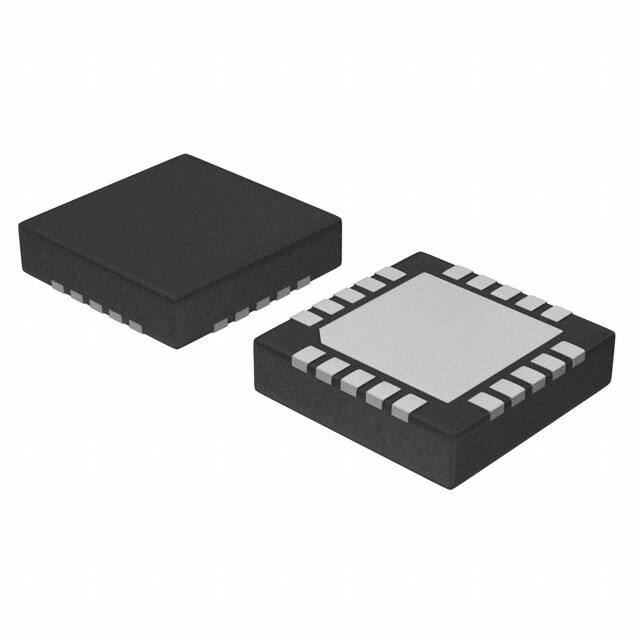
Small QFN Package
These are Pb−Free Devices
http://onsemi.com
MARKING
DIAGRAM
20
QFN20
4 x 4 mm
CASE 485E
1
NCP
1840
ALYWG
G
NCP1840 = Specific Device Code
A
= Assembly Location
L
= Wafer Lot
Y
= Year
W
= Work Week
G
= Pb−Free Package
(*Note: Microdot may be in either location)
ORDERING INFORMATION
Package
Shipping†
NCP1840Q8A6MNG
QFN20
(Pb−Free)
490 / Tray
NCP1840Q8A6MNTWG
QFN20 2500 / Tape &
(Pb−Free)
Reel
Device
†For information on tape and reel specifications,
including part orientation and tape sizes, please
refer to our Tape and Reel Packaging Specifications
Brochure, BRD8011/D.
Typical Applications
• Status or Diagnostic Indicators
•
© Semiconductor Components Industries, LLC, 2013
February, 2013 − Rev. 3
Electronic Musical Instruments
Aftermarket Automotive Trim
♦ Keypad Lighting
Small−Format Display Drivers
♦ Tablet PCs and PDAs
♦ Smart Phones
“True Green” LED Applications
♦
♦
Portables (Notebook Battery Monitors, Handheld
Equipment Testers, etc.)
♦ Computing (Servers, Workstations, etc.)
♦ Electronic Payment Systems
Decorative Lighting
♦ Toys and Gaming − “Fun Lighting”
♦
•
•
1
Publication Order Number:
NCP1840/D
�C1−
C2−
17
16
18 VBAT
19 C2+
20 C1+
NCP1840
CPO
1
15 GND
LED1
2
14 LED8
LED2
3
LED3
4
12 LED6
LED4
5
11
13 LED7
9
SDA
LED5
RBIAS 10
8
SCL
DVCC 7
GND
6
21:GND
(Top View)
Figure 1. Pin Configuration
C1
1 mF
C1+
VBAT
VBAT
C2
1 mF
C1−
C2+
CBAT
2.2 mF
C2−
CPO
RBIAS
RBIAS
10.25 KW
C0
2.2 mF
LED1−8
I2C
2
DVCC
1 mF
8
SCL / SDA
DVCC
GND
Figure 2. Typical NCP1840 Application
http://onsemi.com
2
�Pin 16− C2−
Pin 19− C2+
Pin 17− C1−
Pin 20− C1+
Pin 18− VBAT
NCP1840
Charge Pump
Pin 1− CPO
Oscillator
Pin 10− RBIAS
Bandgap & Bias
Generator
Output DAC
Pin 2− LED1
Output DAC
Pin 3− LED2
Output DAC
Pin 4− LED3
Output DAC
Pin 5− LED4
Output DAC
Pin 11− LED5
Output DAC
Pin 12− LED6
Output DAC
Pin 13− LED7
Output DAC
Pin 14− LED8
Registers
Control Logic
Pin 8− SCL
Pin 9− SDA
Logic Serial
Interface
Pin 7− DVCC
Pin 6− GND
Pin 15− GND
Over Temp Detect
POR
Figure 3. NCP1840 Block Diagram
PIN DESCRIPTION
Pin
Name
Function
1
CPO
Charge pump output used as power supply to the LEDs. Should have a 2.2 mF ceramic
capacitor (X5R or X7R) connected to ground.
2−5, 11−14
LED1 − LED8
Current sink outputs for driving LEDs. Output current level and PWM duty cycle can be
programmed through the I2C interface.
6, 15, 21
GND
Ground connection (Pin 21 is the exposed paddle and should be connected to ground)
7
DVCC
Supply input for digital circuitry. Should have a 1 mF ceramic capacitor (X5R or X7R)
connected to ground.
8
SCL
I2C clock input
9
SDA
I2C serial data input/output
10
RBIAS
An external resistor connected to ground defines the full−scale current for the LED outputs.
16, 17, 19, 20
C2−, C1−, C2+,
C1+
18
VBAT
Charge pump flying capacitor connections. A 1 mF ceramic capacitor (X5R or X7R) should be
connected from C1+ to C1− and C2+ to C2−.
Supply input for the charge pump and analog circuitry. Should have a 2.2 mF low ESR
ceramic capacitor connected to ground.
http://onsemi.com
3
�NCP1840
ABSOLUTE MAXIMUM RATINGS
Symbol
Value
Unit
Battery Supply Voltage Range
Rating
VBAT
−0.3 to 6
V
Digital Supply Voltage Range
DVCC
−0.3 to 6
V
Charge Pump Output Voltage Range
VCPO
−0.3 to 6
V
LED Outputs Voltage Range
VLED
−0.3 to 6
V
SCL Voltage Range
VSCL
−0.3 to (DVCC + 0.3)
V
SDA Voltage Range
VSDA
−0.3 to (DVCC + 0.3)
V
Thermal Resistance, Junction−to−Air (Note 1)
RθJA
66.7
°C/W
Storage Temperature Range
TSTG
−40 to 150
°C
Lead Temperature, Soldering (Note 2)
TSLD
260
°C
ESD Capability, Human Body Model (Note 3)
ESDHBM
2.0
kV
ESD Capability, Machine Model (Note 3)
ESDMM
175
V
ESD Capability, Charged Device Model (Note 3)
ESD Capability, Charged Device Model − Corner Pins (Note 3)
Latch−up Current Immunity (Note 3)
ESDCDM
500
V
ESDCDM−C
750
V
LU
150
mA
Stresses exceeding Maximum Ratings may damage the device. Maximum Ratings are stress ratings only. Functional operation above the
Recommended Operating Conditions is not implied. Extended exposure to stresses above the Recommended Operating Conditions may affect
device reliability.
1. The maximum power dissipation level is the lower of 1) the maximum allowed power dissipation for this particular package, or 2) the power
dissipation at which the junction temperature reaches its maximum operating value.
2. For information, please refer to our Soldering and Mounting Techniques Reference Manual, SOLDERRM/D.
3. Tested by the following methods @ TA = 25°C:
ESD Human Body Model tested per AEC−Q100−002 (EIA/JESD22−A114)
ESD Machine Model tested per EIA/JESD22−A115
ESD Charged Device Model per ESD−STM5.3.1−1999
Latch−up Current Maximum Rating: v100 mA per JEDEC standard: EIA/JESD78
http://onsemi.com
4
�NCP1840
OPERATING RANGES
Symbol
Min
Max
Unit
Battery Supply Voltage
Rating
VBAT
3
5.5
V
Digital Supply Voltage
DVCC
3
5.5
V
Ground
GND
0
V
Vf
4.1
V
20.5
kW
LED Forward Voltage (Note 4)
RBIAS External Resistor
RBIAS
10.25
Ambient Temperature
TA
−40
85
°C
Junction Temperature
TJ
−40
125
°C
4. At full PWM, max current level.
ELECTRICAL CHARACTERISTICS (TJ = 25°C unless otherwise specified)
Symbol
Parameter
Digital Supply Current (Note 5)
Digital Supply Current − Low Power Mode (Note 6)
Battery Supply Current (Note 5)
Battery Supply Current − Low Power Mode (Note 6)
Typ
Max
Unit
IDVCC
Min
2.3
3.1
mA
IDVCC−LOQ
0.6
2
mA
IVBATT
520
750
mA
IVBATT−LOQ
120
500
nA
LED Output Current − Full−Scale (Note 7)
ILED(31)
28
30
34.5
mA
LED Output Current − Zero−Scale (Note 7)
ILED(0)
0.81
0.85
0.95
mA
LED−to−LED Matching (Note 8)
MLED
4
6.9
%
High Level Input Voltage − SDA & SCL Pins
VIH
Low Level Input Voltage − SDA & SCL Pins
VIL
Low Level Input Current − SDA & SCL Pins
IIL
High Level Input Current − SDA & SCL Pins
0.8 *
DVCC
V
0.2 *
DVCC
V
−1.0
1.0
mA
1.0
mA
IIH
−1.0
High Level Output Voltage − SDA Pin
VOH
2.4
Low Level Output Voltage − SDA Pin
VOL
Low Level Output Current − SDA Pin
IOL
High Level Output Current − SDA Pin
IOH
V
0.4
4.0
V
mA
−4.0
mA
5. All LED outputs off, Charge Pump in 1X Mode, no I2C Communication.
6. Part enters Low Power Mode around 5 ms after all LED outputs are OFF and there is no I2C communication. Communication to the part
resumes normal operation in less than 1 ms.
7. With external RBIAS = 10.25 kW on RBIAS pin.
8. For T = −40°C, maximum LED−to−LED matching 7.5%. LED−to−LED Matching is calculated by comparing the output with highest current
against the output with lowest current, divided by the output with lowest current, all at the same programmed value. (Imax − Imin) / Imin.
http://onsemi.com
5
�NCP1840
I2C TIMING CHARACTERISTICS (TJ = 25°C unless otherwise specified)
Symbol
Parameter
Min
Max
Unit
400
kHz
SCL Clock Frequency
fSCL
SCL Low Time
tLOW
1.3
ms
SCL High Time
tHIGH
0.6
ms
Start Hold Time
tHD;STA
0.6
ms
Data Hold Time
tHD;DAT
Start Setup Time
tSU;STA
0.6
ms
Data Setup Time
tSU;DAT
100
ms
Stop Setup Time
tSU;STO
0.6
ms
tBUF
1.3
ms
Rise Time (SCL and SDA)
tR
10
300
ns
Fall Time (SCL and SDA)
tF
10
300
ns
Bus Free Time (Stop and Start Conditions)
0.9
ms
TYPICAL PERFORMANCE CHARACTERISTICS (VBAT = 4.0 V, DVCC = 3.3 V,
IOUT = 160 mA (8 LEDs at 20 mA/ch), CIN = COUT = 2.2 mF, C1 = C2 = 1 mF, TAMB = 25°C unless otherwise specified.)
100
100
VF = 3.25 V
VF = 3.25 V
90
1.5x
EFFICIENCY (%)
EFFICIENCY (%)
90
80
70
60
1x
50
40
2x
1.33x
1.33x
80
1x
70
60
50
5.5
5.0
4.5
4.0
3.5
3.0
2.5
40
2.0
4.2
4.0
3.8
3.6
3.4
3.2
VBAT VOLTAGE (V)
VBAT (Li−Ion) VOLTAGE (V)
Figure 4. Efficiency vs. VBAT Voltage
Figure 5. Efficiency vs. Li−Ion Voltage
http://onsemi.com
6
3.0
�NCP1840
TYPICAL PERFORMANCE CHARACTERISTICS (VBAT = 4.0 V, DVCC = 3.3 V,
IOUT = 160 mA (8 LEDs at 20 mA/ch), CIN = COUT = 2.2 mF, C1 = C2 = 1 mF, TAMB = 25°C unless otherwise specified.)
2.0
LED CURRENT CHANGE (%)
LED CURRENT CHANGE (%)
6
VDCC = 3.3 V
4
2
0
−2
−4
−6
2.0
2.5
3.0
3.5
4.0
4.5
5.0
1.5
1.0
0.5
0
−0.5
−1.0
−1.5
−2.0
5.5
2.5
3.0
3.5
4.0
4.5
VBAT VOLTAGE (V)
DVCC VOLTAGE (V)
Figure 6. LED Current Change vs. VBAT
Voltage
Figure 7. LED Current Change vs. DVCC
Voltage
Figure 8. Power Up in 1x Mode,
ILED = 30 mA/ch
Figure 9. Power Up in 1.33x Mode,
ILED = 30 mA/ch
LED CURRENT (%)
100
10
1
1
10
100
PWM DUTY CYCLE (%)
Figure 10. LED Current vs. PWM Duty Cycle
Figure 11. PWM Waveform, 50% Duty Cycle,
ILED = 30 mA/ch
http://onsemi.com
7
5.0
�NCP1840
OPERATION DESCRIPTION
Constant Current Control
Additionally, the NCP1840 allows for the current through
each of the 8 channels to be fully programmable via a 5−bit
DAC on each output, allowing for the desired luminance to
be achieved for each channel. Programming the current
level is achieved by loading data into channel−specific
registers through the I2C serial interface. The output current
levels are logarithmic, providing a perceived linear LED
brightness to the human eye, as shown in Figure 12. This
allows for a more gradual and natural viewing change in
LED brightness between levels.
The NCP1840 has 8 LED channels that are individually
regulated constant current sources. The maximum current
per channel is 30 mA but can be reduced by adjusting the
resistor RBIAS, which is placed between the RBIAS pin and
ground. RBIAS is required and can vary between 10.25 kW
and 20.5 kW. The maximum current per channel can be
calculated with the following equation:
I max + 250 *
1.23 V
R BIAS
High
30
25
Perceived
Brightness
OUTPUT CURRENT LEVEL (mA)
35
20
15
10
Low
5
0
0
1 3 5 7 9 11 13 15 17 19 21 23 25 27 29 31
DAC Level
31
Figure 12. Logarithmic Output Current (RBIAS = 10.25 KW)
PWM Control
switches into 1.33x mode. In this mode, the output voltage
is approximately equal to 1.33 times the input supply
voltage. If the input voltage is insufficient again to maintain
current regulation in all active channels, the device will
automatically switch to the 1.5x mode. In this mode, the
output voltage will be approximately equal to 1.5 times the
input supply voltage. If the input voltage is still insufficient
to maintain the constant current regulation in all active
channels, the device will automatically switch to the 2x
mode where the output voltage is approximately equal to
two times the input supply voltage. In all modes, if the
device detects a sufficient input voltage to drive all LED
currents in 1x mode, it will automatically change back to 1x
mode to optimize efficiency.
The NCP1840 provides 6−bit PWM duty cycle control for
each of its 8 channels, allowing each channel to be dimmed
independent of the other channels and without sacrificing
the LED color output. Programming PWM duty cycle is
achieved by loading data into channel−specific registers
through the I2C serial interface. The typical on time of the
LED can be calculated by multiplying the duty cycle
percentage by the typical PWM period of 575 ms.
Charge Pump
The NCP1840 incorporates a high efficiency, low noise,
QUAD−MODE (1x, 1.33x, 1.5x, and 2x) charge pump. This
allows for higher forward voltage LEDs and/or multiple
LEDs in series per channel to be driven with a low−voltage
supply. In order to optimize efficiency while maintaining
constant current regulation, the NCP1840 automatically
senses when it should change charge pump modes based on
the voltage across the LED current sources. By utilizing the
1.33x mode, approximately 10% more efficiency than a
typical 1.5x mode is achieved.
The NCP1840 powers up in 1x mode where the charge
pump output voltage will be approximately equal to the
input supply voltage. If the output voltage is sufficient to
regulate all LED currents, the device remains in this mode.
However, if the input voltage is insufficient to regulate the
current in all active channels, the device automatically
I2C Serial Interface
The registers of the NCP1840 are programmed and read
through an I2C serial interface. Due to the NCP1840 only
being configured as a Slave device, a Master device is
required on the communication bus. The NCP1840 has a
factory programmed 7−bit Slave address of 0011011 (1B
hex). The last bit of the Slave address specifies whether a
Read (1) or Write (0) operation is to be performed. The
maximum clock frequency for the serial interface is 400 kHz
and both the SCL and SDA lines require external pull−up
resistors.
http://onsemi.com
8
�NCP1840
Register Writes & Reads
byte to be written. The NCP1840 then acknowledges the
received register data and the Master issues a STOP
condition to terminate the communication.
The ability of the NCP1840 to allow the internal registers
to be both written and read provides the user with the benefit
of being able to easily verify correct register writes and
isolate system problem areas while troubleshooting. This
ability also allows users to configure the register values
according to desired LED performance, read these register
values from the part, and then store these settings in external
memory for future use. In addition, an over−temperature
fault condition can also be read from a specific register,
allowing for diagnostic feedback to the system controller.
Read Protocol
The Read protocol that is used by the NCP1840 is depicted
in Figure 14. As can be seen, the Master initiates the
communication by issuing a START condition and then by
broadcasting the 7−bit part address of the NCP1840
followed by a Write operation request (0). This is because
the control bits need to first be set to 001 before a read
operation takes place. The NCP1840 acknowledges the
request and the Master then transmits the address byte which
consists of 001, for the 3 control bits, followed by the 5−bit
address of the register to be read from. Upon successful
receipt of the address byte, the NCP1840 acknowledges to
the Master which will then issue another START condition
followed by the 7−bit part address of the NCP1840 and a
Read operation request (1). The NCP1840 acknowledges
the request and then transmits the data byte to be read by the
Master. The NCP1840 then releases the SDA line and the
Master terminates the Read session by not acknowledging
the data byte and by issuing a STOP condition.
Write Protocol
The Write protocol that is used by the NCP1840 is
depicted in Figure 13. As can be seen, the Master initiates
the communication by issuing a START condition and then
by broadcasting the 7−bit part address of the NCP1840
followed by a Write operation request (0). The NCP1840
acknowledges the request and then the Master transmits the
address byte which consists of 3−bits of control data
followed by the 5−bit address of the register to be written to.
Upon successful receipt of the address byte, the NCP1840
acknowledges to the Master which then transmits the data
WRITE PROTOCOL USED BY NCP1840:
1
7
1
1
3
5
1
8
1
1
S
Part Address
W
A
Control Bits
Register Address
A
Register
Data
A
P
S = Start Condition, W = Write, A = Acknowledge, P = Stop Condition
Part Address
Control Bits
START
Register Address
Register Data
STOP
WRITE
0
0
1
1
2
1
3
0
4
1
5
1
6
0
7
ACK CB2 CB1 CB0
8
9
1
2
3
A4
A3
A2
A1
A0
4
5
6
7
8
ACK
9
D7
D6
D5
D4
D3
D2
D1
D0
1
2
3
4
5
6
7
8
ACK
9
Figure 13. NCP1840 Write Protocol
READ PROTOCOL USED BY NCP1840:
1
7
1
1
3
5
1
8
7
1
1
8
1
1
S
Part Address
W
A
Control Bits
Register
Address
A
S
Part Address
R
A
Register
Data Out
A
P
S = Start Condition, W = Write, R = Read, A = Acknowledge, A =No Acknowledge, P = Stop Condition
Control Bits
Part Address
Register Address
0
1
0
1
2
3
1
0
4
1
5
1
6
0
7
START
ACK
8
Register Data Out
Part Address
WRITE
START
9
0
1
0
2
1
3
A4
A3
A2
A1
A0
4
5
6
7
8
ACK
0
0
1
9
1
2
1
3
0
4
1
5
1
6
Figure 14. NCP1840 Read Protocol
http://onsemi.com
9
STOP
READ
1
7
8
ACK
D7
D6
D5
D4
D3
D2
D1
D0
ACK
9
1
2
3
4
5
6
7
8
9
�NCP1840
Control Bits
table contains a description of each of these functions along
with their dependencies on the register address, A[4:0], and
the data byte, D[7:0].
The NCP1840 has 3 control bits that are used to dictate the
function that will be performed by the part. The following
CONTROL BITS DESCRIPTION
CB2
CB1
CB0
Function
0
0
0
Turn all LED Channels ON/OFF
All channels are turned ON/OFF according to the data in the Output Control Register. The current and PWM
duty cycle will depend on each channel’s Current Level and PWM Register. The register address field, A[4:0],
is ignored along with the data byte, D[7:0]. The Master can issue a STOP condition without sending a data
byte.
0
0
1
Program a Single Register (also Read Operation Setting)
The register address, A[4:0], defines the register to be written or read. For a write, the data byte, D[7:0],
defines the data to be written. The data will be loaded in the register but will not take effect until either a 000 or
010 Control Bit setting is applied. This is also the Control Bit setting required for a Read operation (see Read
Protocol).
0
1
0
Program a Single Register and Turn all LED Channels ON/OFF
The register address, A[4:0], defines the register to be written to and the data byte, D[7:0], defines the data to
be written. After the receipt of the data byte, all channels will be turned ON/OFF according to the data in the
Output Control Register. The current and PWM duty cycle will depend on each channel’s Current Level and
PWM Register.
0
1
1
Program all 8 Current Level Registers
All Current Level Registers will be loaded with the data defined by the data byte, D[7:0]. The register address,
A[4:0], is ignored. The data will be loaded in the registers but will not take effect until either a 000 or 010 Control Bit setting is applied.
1
0
0
Program all 8 PWM Registers
All PWM Registers will be loaded with the data defined by the data byte, D[7:0]. The register address, A[4:0],
is ignored. The data will be loaded in the registers but will not take effect until either a 000 or 010 Control Bit
setting is applied.
1
0
1
Reserved
1
1
0
Reserved
1
1
1
Reserved
Register Address Map
Level Registers are used to program the output current for
each of the 8 channels. The 8 PWM Registers are used to
program the PWM duty cycle for each of the 8 channels. The
Output Control Register is used to set the status, either ON
or OFF, of all 8 channels. The Main Status Register is used
to indicate the operating condition of the part: normal
operation, low power mode, or over temperature.
The NCP1840 has a total of 18 different register
addresses, as shown in the table below, made up of the
following: 8 addresses for the individual channel Current
Level Registers, 8 addresses for the individual channel
PWM Registers, 1 address for the Output Control Register,
and 1 address for the Main Status Register. The 8 Current
REGISTER ADDRESS MAP
Address − Binary
A4
A3
A2
A1
A0
Address − Hex
0
0
0
0
0
0
LED1 Current Level Register
0
0
0
0
1
1
LED2 Current Level Register
0
0
0
1
0
2
LED3 Current Level Register
0
0
0
1
1
3
LED4 Current Level Register
0
0
1
0
0
4
LED5 Current Level Register
0
0
1
0
1
5
LED6 Current Level Register
0
0
1
1
0
6
LED7 Current Level Register
0
0
1
1
1
7
LED8 Current Level Register
0
1
0
0
0
8
LED1 PWM Register
0
1
0
0
1
9
LED2 PWM Register
Function
http://onsemi.com
10
�NCP1840
REGISTER ADDRESS MAP
Address − Binary
A4
A3
A2
A1
A0
Address − Hex
0
1
0
1
0
A
LED3 PWM Register
0
1
0
1
1
B
LED4 PWM Register
0
1
1
0
0
C
LED5 PWM Register
0
1
1
0
1
D
LED6 PWM Register
0
1
1
1
0
E
LED7 PWM Register
0
1
1
1
1
F
LED8 PWM Register
1
0
0
0
0
10
Output Control Register
1
0
0
0
1
11
Main Status Register
Function
Current Level Registers
that are implemented as a logarithmically scaled percentage
of the maximum current, dictated by an external resistor
RBIAS. A description of the 32 different current levels can be
found in the following table.
The current through each of the 8 channels on the
NCP1840 can be individually programmed by loading the
appropriate data into the Current Level Register for each
channel. There are 32 different current levels per channel
CURRENT LEVEL REGISTER DESCRIPTION
Data − Binary
D7
D6
D5
D4
D3
D2
D1
D0
Data − Hex
Percentage of Maximum Current
0
0
0
0
0
0
0
0
00
2.8333%
0
0
0
0
0
0
0
1
01
3.1667%
0
0
0
0
0
0
1
0
02
3.5333%
0
0
0
0
0
0
1
1
03
3.9667%
0
0
0
0
0
1
0
0
04
4.4667%
0
0
0
0
0
1
0
1
05
5.0000%
0
0
0
0
0
1
1
0
06
5.6333%
0
0
0
0
0
1
1
1
07
6.3000%
0
0
0
0
1
0
0
0
08
7.0667%
0
0
0
0
1
0
0
1
09
7.9333%
0
0
0
0
1
0
1
0
0A
8.9000%
0
0
0
0
1
0
1
1
0B
10.0000%
0
0
0
0
1
1
0
0
0C
11.2333%
0
0
0
0
1
1
0
1
0D
12.6000%
0
0
0
0
1
1
1
0
0E
14.1333%
0
0
0
0
1
1
1
1
0F
15.8667%
0
0
0
1
0
0
0
0
10
17.8000%
0
0
0
1
0
0
0
1
11
19.9667%
0
0
0
1
0
0
1
0
12
22.4000%
0
0
0
1
0
0
1
1
13
25.1333%
0
0
0
1
0
1
0
0
14
28.2000%
0
0
0
1
0
1
0
1
15
31.6333%
0
0
0
1
0
1
1
0
16
35.4667%
0
0
0
1
0
1
1
1
17
39.8000%
http://onsemi.com
11
�NCP1840
CURRENT LEVEL REGISTER DESCRIPTION
Data − Binary
D7
D6
D5
D4
D3
D2
D1
D0
Data − Hex
Percentage of Maximum Current
0
0
0
1
1
0
0
0
18
44.6667%
0
0
0
1
1
0
0
1
19
50.2333%
0
0
0
1
1
0
1
0
1A
56.2333%
0
0
0
1
1
0
1
1
1B
63.1000%
0
0
0
1
1
1
0
0
1C
70.8000%
0
0
0
1
1
1
0
1
1D
79.4333%
0
0
0
1
1
1
1
0
1E
89.1333%
0
0
0
1
1
1
1
1
1F
100.0000%
PWM Registers
100%, fully ON. A description of the 64 different PWM duty
cycle settings can be found in the following table. Note that
the typical on time of the LED can be calculated by
multiplying the duty cycle percentage by the typical PWM
period of 575 ms.
The PWM duty cycle of each of the 8 channels on the
NCP1840 can be individually programmed by loading the
appropriate data into the PWM Register for each channel.
There are 64 different duty cycle settings per channel that are
implemented in a linear fashion from 0%, fully OFF, to
PWM REGISTER DESCRIPTION
Data − Binary
D7
D6
D5
D4
D3
D2
D1
D0
Data − Hex
PWM Duty Cycle
0
0
0
0
0
0
0
0
00
0.000%
0
0
0
0
0
0
0
1
01
1.587%
0
0
0
0
0
0
1
0
02
3.175%
0
0
0
0
0
0
1
1
03
4.762%
0
0
0
0
0
1
0
0
04
6.349%
0
0
0
0
0
1
0
1
05
7.937%
0
0
0
0
0
1
1
0
06
9.524%
0
0
0
0
0
1
1
1
07
11.111%
0
0
0
0
1
0
0
0
08
12.698%
0
0
0
0
1
0
0
1
09
14.286%
0
0
0
0
1
0
1
0
0A
15.873%
0
0
0
0
1
0
1
1
0B
17.460%
0
0
0
0
1
1
0
0
0C
19.048%
0
0
0
0
1
1
0
1
0D
20.635%
0
0
0
0
1
1
1
0
0E
22.222%
0
0
0
0
1
1
1
1
0F
23.810%
0
0
0
1
0
0
0
0
10
25.397%
0
0
0
1
0
0
0
1
11
26.984%
0
0
0
1
0
0
1
0
12
28.571%
0
0
0
1
0
0
1
1
13
30.159%
0
0
0
1
0
1
0
0
14
31.746%
0
0
0
1
0
1
0
1
15
33.333%
0
0
0
1
0
1
1
0
16
34.921%
http://onsemi.com
12
�NCP1840
PWM REGISTER DESCRIPTION
Data − Binary
D7
D6
D5
D4
D3
D2
D1
D0
Data − Hex
PWM Duty Cycle
0
0
0
1
0
1
1
1
17
36.508%
0
0
0
1
1
0
0
0
18
38.095%
0
0
0
1
1
0
0
1
19
39.683%
0
0
0
1
1
0
1
0
1A
41.270%
0
0
0
1
1
0
1
1
1B
42.857%
0
0
0
1
1
1
0
0
1C
44.444%
0
0
0
1
1
1
0
1
1D
46.032%
0
0
0
1
1
1
1
0
1E
47.619%
0
0
0
1
1
1
1
1
1F
49.206%
0
0
1
0
0
0
0
0
20
50.794%
0
0
1
0
0
0
0
1
21
52.381%
0
0
1
0
0
0
1
0
22
53.968%
0
0
1
0
0
0
1
1
23
55.556%
0
0
1
0
0
1
0
0
24
57.143%
0
0
1
0
0
1
0
1
25
58.730%
0
0
1
0
0
1
1
0
26
60.317%
0
0
1
0
0
1
1
1
27
61.905%
0
0
1
0
1
0
0
0
28
63.492%
0
0
1
0
1
0
0
1
29
65.079%
0
0
1
0
1
0
1
0
2A
66.667%
0
0
1
0
1
0
1
1
2B
68.254%
0
0
1
0
1
1
0
0
2C
69.841%
0
0
1
0
1
1
0
1
2D
71.729%
0
0
1
0
1
1
1
0
2E
73.016%
0
0
1
0
1
1
1
1
2F
74.603%
0
0
1
1
0
0
0
0
30
76.190%
0
0
1
1
0
0
0
1
31
77.778%
0
0
1
1
0
0
1
0
32
79.365%
0
0
1
1
0
0
1
1
33
80.952%
0
0
1
1
0
1
0
0
34
82.540%
0
0
1
1
0
1
0
1
35
84.127%
0
0
1
1
0
1
1
0
36
85.714%
0
0
1
1
0
1
1
1
37
87.302%
0
0
1
1
1
0
0
0
38
88.889%
0
0
1
1
1
0
0
1
39
90.476%
0
0
1
1
1
0
1
0
3A
92.063%
0
0
1
1
1
0
1
1
3B
93.651%
0
0
1
1
1
1
0
0
3C
95.238%
0
0
1
1
1
1
0
1
3D
96.825%
0
0
1
1
1
1
1
0
3E
98.413%
0
0
1
1
1
1
1
1
3F
100.000%
http://onsemi.com
13
�NCP1840
Output Control Register
OFF with a 0 loaded into that bit. When an LED channel is
turned ON, the current level and PWM duty cycle of that
channel will be dictated by the data that is loaded into its
Current Level Register and PWM Register. It is important to
note that any unused LED channel should not be turned ON.
The Output Control Register on the NCP1840 is used to
set the status, either ON or OFF, of all 8 channels. As shown
in the following table, each bit in the register corresponds to
one of the 8 LED channels. Each channel will be turned ON
with a 1 loaded into the corresponding bit and will be turned
OUTPUT CONTROL REGISTER DESCRIPTION
Register Bit (1 = ON, 0 = OFF)
D7
D6
D5
D4
D3
D2
D1
D0
Corresponding LED Channel
LED8
LED7
LED6
LED5
LED4
LED3
LED2
LED1
Main Status Register
condition currently exists on the part. Likewise, bit D2
indicates either normal operation (0) or low power mode
operation (1). When all LED outputs are turned OFF and
there is no I2C communication for 5 ms, the part will put
itself in a low power mode and set bit D2 to a logic one.
When the Master wakes the device up with I2C
communication, bit D2 will be set to a logic zero once the
entire chip is ready to run in normal operation. Therefore,
when the Master wakes up the device, it can read bit D2 and
wait for this bit to change to 0, indicating the return to normal
operation.
The Main Status Register of the NCP1840 is used to
indicate the operating condition of the part and is read−only.
As shown in the following table, bit D0 indicates either
normal operation (0) or an over temperature condition (1).
When the on−chip temperature sensor detects an
over−temperature condition, it will turn off all LED outputs,
along with the charge pump, and set bit D0 to a logic one. If
the over−temperature condition goes away, bit D0 will
automatically reset to a logic zero and the part will resume
normal operation. Therefore, bit D0 of this register can be
read and used to help determine if an over−temperature
MAIN STATUS REGISTER DESCRIPTION
D7
D6
D5
D4
D3
0
0
0
0
0
D2
D1
0 = Normal Operation
0
1 = Low Power Mode
Fault Management
The NCP1840 has several fault management features
intended to provide increased performance and reliability to
both the system and the part itself:
• Each LED output will detect if it is shorted to the
charge pump output and if so will turn that particular
channel’s circuitry OFF. This saves power consumption
that would otherwise be lost and provides the user with
the ability to ensure that unused channels are turned
OFF by tying them to the charge pump output.
• The charge pump output will detect any over−current
events and automatically limit the current to less than
800 mA. This helps to prevent any damage to the chip
and the system due to elevated current on this output.
• The charge pump output will detect a short−circuit
event (less than 0.7 V) and limit the current to the
soft−start limit of less than 94 mA. This helps to
prevent damage to the chip and the system that could
potentially be seen with the output being
short−circuited to ground.
• The charge pump will reset itself to 1x mode if it
reaches an overvoltage level (5.5 V to 6 V). This helps
to prevent damage to the chip and the system in the
•
•
0 = Normal Operation
1 = Over Temperature
event that the supply voltage increases while the charge
pump is operating in the 1.33x, 1.5x, or 2x mode.
If the external resistor, RBIAS, used to set the maximum
output current and the internal reference current, is too
small or otherwise short−circuits, the NCP1840 will
detect this over−current condition and turn off the
reference current and LED outputs. This helps to
prevent damage to the chip and system due to elevated
currents that would be present.
The NCP1840 has an on−chip over temperature sensor
that will detect any over−temperature condition (130°C
− 163°C) and turn off all LED outputs along with the
charge pump. In an over−temperature state, bit D0 of
the Main Status Register will be set to a logic one.
When the over−temperature condition goes away, the
part will resume normal operation and bit D0 will be set
to a logic zero. The D0 bit of the Main Status Register
can be read through the I2C interface and can be used to
provide feedback to the Master controller. This helps to
protect the chip and system in the event that the
temperature increases beyond a safe operating
condition.
http://onsemi.com
14
D0
�NCP1840
power mode, the I2C interface is still active and all register
settings are retained, but the charge pump and other circuitry
that is not needed is powered down. Bit D2 of the Main
Status Register is set to a logic one during low power mode.
The part is brought out of this mode when the Master
initiates communication with it via the I2C interface. When
this happens, the part returns to normal operation and bit D2
is set to a logic zero. Therefore, when the Master wakes up
the device, it can read bit D2 and wait for this bit to change
to 0, indicating that all circuitry is back to full operation. The
transition period from when the part receives the wake−up
to full normal operation takes less than 1 ms.
Soft Start−Up
The NCP1840 has an on−chip power−on−reset (POR)
circuitry that is used to provide soft start−up. As the supply
voltage is applied, the POR will sense when the voltage
reaches a level that will allow all circuitry to operate
correctly. It then will gradually apply this supply voltage to
the chip to minimize noise and reduce EMI. If during
operation the supply voltage drops, the POR will ensure that
the part is reset before the voltage reaches a level where the
circuitry won’t operate as intended. This helps to mitigate
strange operation during a power glitch or brown−out
situation.
All registers are reset to all zeros on start−up.
Unused LED Channels
Low Power Mode
Any of the 8 LED channels that are not needed should be
tied to the charge pump output to ensure that these channels
remain OFF and to save power consumption that would
otherwise be lost.
The NCP1840 minimizes power consumption by entering
into low power mode about 5 ms after all LED outputs are
turned OFF and there is no I2C communication. During low
EXAMPLE
Objective: To set the currents for each LED, except LED8, to 1.5 mA. LED8 will be set to 3.0 mA. All LEDs will have
a 50% PWM duty cycle. After these registers are loaded, then only LEDs 1, 2, 3, 4, and 8 will be activated. Later,
LED8 will be turned off. Lastly the PWM register value for LED1 will be read. Note that RBIAS = 10.25 kW for this
example.
Step 1. Set the current level for ALL LEDs to 1.5 mA.
1.1 Set the Part Address to 1B (hex).
1.2 Set the Read/Write bit to 0.
1.3 Set the Control Bits to 011 to program all Current Level Registers at the same time.
1.4 Set the Data to 05 (hex), which will set the current to 1.5 mA.
Start
S
Part Address
0011011
R/W
0
Ack
A
Control
Bits
011
Register Address
Don’t Care
Ack
A
Register Data
00000101
Ack
A
Stop
P
Step 2. Set the current level for LED8 to 3.0 mA.
2.1 Set the Part Address to 1B (hex).
2.2 Set the Read/Write bit to 0.
2.3 Set the Control Bits to 001 and set the Register address to 07 (hex) to write to LED8 Current Level Register.
2.4 Set the Data to 0B (hex), which will set the current to 3.0 mA.
Start
S
Part Address
0011011
R/W
0
Ack
A
Control
Bits
001
Register Address
00111
Ack
A
Register Data
00001011
Ack
A
Stop
P
Step 3. Set the PWM duty cycle for all LEDs to 50%.
3.1 Set the Part Address to 1B (hex).
3.2 Set the Read/Write bit to 0.
3.3 Set the Control Bits to 100 to program all PWM Registers at the same time.
3.4 Set the Data to 20 (hex), which will set the PWM duty cycle to 50%.
Start
S
Part Address
0011011
R/W
0
Ack
A
Control
Bits
100
Register Address
Don’t Care
http://onsemi.com
15
Ack
A
Register Data
00100000
Ack
A
Stop
P
�NCP1840
Step 4a. Set LEDs 1, 2, 3, 4, 8 to be ON and immediately activate the change with settings loaded in Steps 1−3.
4a.1 Set the Part Address to 1B (hex).
4a.2 Set the Read/Write bit to 0.
4a.3 Set the Control Bits to 010 and set the Register address to 10 (hex) to write to the Output Control Register.
4a.4 Set the Data to 8F (hex), which will set LEDs 1, 2, 3, 4, 8 to be ON.
Note: After this step the LEDs will immediately be activated with the current level and PWM duty cycle settings previously
loaded.
Start
S
Part Address
0011011
R/W
0
Ack
A
Control
Bits
010
Register Address
10000
Ack
A
Register Data
Ack
10001111
Stop
A
P
Step 4b. (Alternative to Step 4a.) Set LEDs 1, 2, 3, 4, 8 to be ON and later activate the change with settings loaded in Steps
1−3.
4b.1 Set the Part Address to 1B (hex).
4b.2 Set the Read/Write bit to 0.
4b.3 Set the Control Bits to 001 and set the Register address to 10 (hex) to write to the Output Control Register.
4b.4 Set the Data to 8F (hex), which will set LEDs 1, 2, 3, 4, 8 to be ON.
Note: After this step the LEDs will not be activated until either a 000 or 010 Control Bit setting is applied − see further 4b steps.
Start
S
Part Address
0011011
R/W
0
Ack
A
Control
Bits
001
Register Address
10000
Ack
A
Register Data
Ack
10001111
Stop
A
P
4b.5 Set the Part Address to 1B (hex).
4b.6 Set the Read/Write bit to 0.
4b.7 Set the Control Bits to 000.
Note: After this step the LEDs will immediately be activated with the current level and PWM duty cycle settings previously
loaded.
Start
S
Part Address
0011011
R/W
0
Ack
A
Control
Bits
Register Address
000
Ack
Don’t Care
Stop
A
P
Step 5. Turn OFF LED8, leaving LEDs 1, 2, 3, 4 ON.
5.1 Set the Part Address to 1B (hex).
5.2 Set the Read/Write bit to 0.
5.3 Set the Control Bits to 010 and set the Register address to 10 (hex) to write to the Output Control Register.
5.4 Set the Data to 0F (hex), which will set LED8 OFF and leave LEDs 1, 2, 3, 4 ON.
Start
S
Part Address
0011011
R/W
0
Ack
A
Control
Bits
010
Register Address
10000
http://onsemi.com
16
Ack
A
Register Data
00001111
Ack
A
Stop
P
�NCP1840
Step 6. Read back the LED1 PWM Register value.
6.1 Set the part address to 1B (hex).
6.2 Set the Read/Write bit to 0.
6.3 Set the Controls Bits to 001 in order to perform a Read operation.
6.4 Set the Register Address to 08 (hex) in order to read LED1 PWM Register.
6.5 Issue another Start and set the part address to 1B (hex).
6.6 Set the Read/Write bit to 1.
Note: After this step, the NCP1840 will transmit the LED1 PWM Register data byte which should be 20 (hex).
Start
S
Part Address
0011011
R/W
0
Ack
A
Control Register
Bits
Address Ack Start
001
01000
A
S
Part Address
0011011
R/W
1
Ack
A
Register
Data
Data Out
Ack
notA
LAYOUT CONSIDERATIONS
Some key layout guidelines are as follows:
1. The NCP1840 requires a low−inductance ground.
2. Connect Pin 6 and Pin 15 to the “ground pad” of the NCP1840’s package − see Figure 15.
3. Place vias on the “ground pad,” connecting the GND of the NCP1840 directly to the PCB ground plane − see
Figure 15.
Figure 15. Ground Connection Recommendation
http://onsemi.com
17
Stop
P
�NCP1840
4. Use good−quality X5R or X7R ceramic capacitors for C0, C1, C2, and CBAT − see Figure 16.
Figure 16. Schematic Showing Charge Pump and Decoupling Capacitors
5. Charge pump capacitors C0, C1, C2, and decoupling capacitor CBAT should be as physically close to the NCP1840 as
possible − see Figure 17.
Figure 17. C0, C1, C2, and CBAT Layout Recommendation
QUAD−MODE is a registered trademark of Semiconductor Components Industries, LLC (SCILLC).
http://onsemi.com
18
�MECHANICAL CASE OUTLINE
PACKAGE DIMENSIONS
QFN20, 4x4, 0.5P
CASE 485E
ISSUE C
DATE 13 FEB 2018
SCALE 2:1
A
B
D
PIN ONE
REFERENCE
2X
0.15 C
ÉÉ
ÉÉ
EXPOSED
COPPER
ÉÉ
ÉÉ
ÇÇ
A3
A1
E
ÉÉÉ
ÉÉÉ
ÇÇÇ
A3
MOLD
COMPOUND
PLATING
A1
NOTES:
1. DIMENSIONING AND TOLERANCING PER ASME
Y14.5M, 1994.
2. CONTROLLING DIMENSION: MILLIMETERS.
3. DIMENSION b APPLIES TO PLATED TERMINAL
AND IS MEASURED BETWEEN 0.15 AND 0.30 MM
FROM THE TERMINAL TIP.
4. COPLANARITY APPLIES TO THE EXPOSED PAD
AS WELL AS THE TERMINALS.
DETAIL B
ALTERNATE
CONSTRUCTIONS
DIM
A
A1
A3
b
D
D2
E
E2
e
K
L
L1
2X
0.15 C
L
L
TOP VIEW
(A3)
DETAIL B
L1
A
0.10 C
DETAIL A
OPTIONAL CONSTRUCTIONS
0.08 C
A1
SIDE VIEW
C
SEATING
PLANE
GENERIC
MARKING DIAGRAM*
20
0.10 C A B
D2
DETAIL A
20X
1
L
6
0.10 C A B
11
E2
20
20X
e
b
0.10 C A B
0.05 C
NOTE 3
BOTTOM VIEW
*This information is generic. Please refer to
device data sheet for actual part marking.
Pb−Free indicator, “G” or microdot “ G”,
may or may not be present. Some products
may not follow the Generic Marking.
SOLDERING FOOTPRINT*
4.30
XXXXXX
XXXXXX
ALLYWG
G
XXXXXX= Specific Device Code
A
= Assembly Location
LL
= Wafer Lot
Y
= Year
W
= Work Week
G
= Pb−Free Package
(Note: Microdot may be in either location)
1
K
MILLIMETERS
MIN
MAX
0.80
1.00
--0.05
0.20 REF
0.20
0.30
4.00 BSC
2.60
2.90
4.00 BSC
2.60
2.90
0.50 BSC
0.20 REF
0.35
0.45
0.00
0.15
20X
0.58
2.88
1
2.88 4.30
PKG
OUTLINE
20X
0.35
0.50
PITCH
DIMENSIONS: MILLIMETERS
*For additional information on our Pb−Free strategy and soldering
details, please download the ON Semiconductor Soldering and
Mounting Techniques Reference Manual, SOLDERRM/D.
DOCUMENT NUMBER:
DESCRIPTION:
98AON03163D
QFN20, 4X4, 0.5P
Electronic versions are uncontrolled except when accessed directly from the Document Repository.
Printed versions are uncontrolled except when stamped “CONTROLLED COPY” in red.
PAGE 1 OF 1
onsemi and
are trademarks of Semiconductor Components Industries, LLC dba onsemi or its subsidiaries in the United States and/or other countries. onsemi reserves
the right to make changes without further notice to any products herein. onsemi makes no warranty, representation or guarantee regarding the suitability of its products for any particular
purpose, nor does onsemi assume any liability arising out of the application or use of any product or circuit, and specifically disclaims any and all liability, including without limitation
special, consequential or incidental damages. onsemi does not convey any license under its patent rights nor the rights of others.
© Semiconductor Components Industries, LLC, 2019
www.onsemi.com
�onsemi,
, and other names, marks, and brands are registered and/or common law trademarks of Semiconductor Components Industries, LLC dba “onsemi” or its affiliates
and/or subsidiaries in the United States and/or other countries. onsemi owns the rights to a number of patents, trademarks, copyrights, trade secrets, and other intellectual property.
A listing of onsemi’s product/patent coverage may be accessed at www.onsemi.com/site/pdf/Patent−Marking.pdf. onsemi reserves the right to make changes at any time to any
products or information herein, without notice. The information herein is provided “as−is” and onsemi makes no warranty, representation or guarantee regarding the accuracy of the
information, product features, availability, functionality, or suitability of its products for any particular purpose, nor does onsemi assume any liability arising out of the application or use
of any product or circuit, and specifically disclaims any and all liability, including without limitation special, consequential or incidental damages. Buyer is responsible for its products
and applications using onsemi products, including compliance with all laws, regulations and safety requirements or standards, regardless of any support or applications information
provided by onsemi. “Typical” parameters which may be provided in onsemi data sheets and/or specifications can and do vary in different applications and actual performance may
vary over time. All operating parameters, including “Typicals” must be validated for each customer application by customer’s technical experts. onsemi does not convey any license
under any of its intellectual property rights nor the rights of others. onsemi products are not designed, intended, or authorized for use as a critical component in life support systems
or any FDA Class 3 medical devices or medical devices with a same or similar classification in a foreign jurisdiction or any devices intended for implantation in the human body. Should
Buyer purchase or use onsemi products for any such unintended or unauthorized application, Buyer shall indemnify and hold onsemi and its officers, employees, subsidiaries, affiliates,
and distributors harmless against all claims, costs, damages, and expenses, and reasonable attorney fees arising out of, directly or indirectly, any claim of personal injury or death
associated with such unintended or unauthorized use, even if such claim alleges that onsemi was negligent regarding the design or manufacture of the part. onsemi is an Equal
Opportunity/Affirmative Action Employer. This literature is subject to all applicable copyright laws and is not for resale in any manner.
PUBLICATION ORDERING INFORMATION
LITERATURE FULFILLMENT:
Email Requests to: orderlit@onsemi.com
onsemi Website: www.onsemi.com
◊
TECHNICAL SUPPORT
North American Technical Support:
Voice Mail: 1 800−282−9855 Toll Free USA/Canada
Phone: 011 421 33 790 2910
Europe, Middle East and Africa Technical Support:
Phone: 00421 33 790 2910
For additional information, please contact your local Sales Representative
�


 工商网监
湘ICP备2023018690号
工商网监
湘ICP备2023018690号
