Voltage Regulator - Low Iq,
Low Dropout, Power Good
Output
1.2 A
NCP187
www.onsemi.com
The NCP187 is 1.2 A LDO Linear Voltage Regulator. It is a very
stable and accurate device with low quiescent current consumption
(typ. 30 mA over the full temperature range), low dropout, low output
noise and very good PSRR. The regulator incorporates several
protection features such as Thermal Shutdown, Soft Start, Current
Limiting and also Power Good Output signal for easy MCU
interfacing.
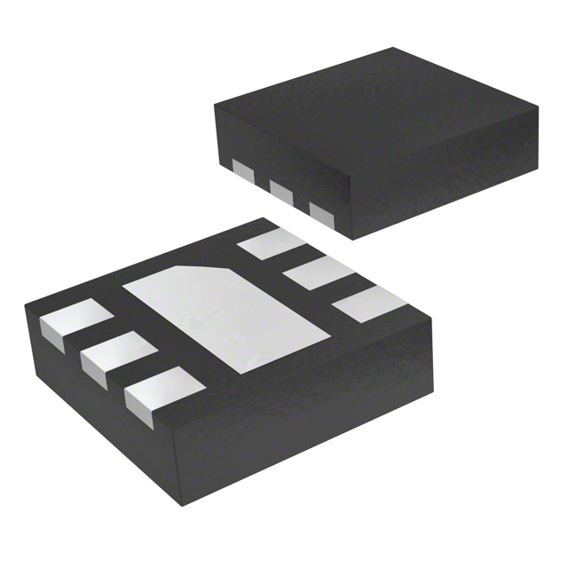
WDFN6/WDFNW6 2x2
CASES 511BR & 511DW
Features
•
•
•
•
•
•
•
•
•
•
•
•
Operating Input Voltage Range: 1.5 V to 5.5 V
Adjustable and Fixed Voltage Options Available: 0.8 V to 5.2 V
Low Quiescent Current: typ. 30 mA over Temperature
±2% Accuracy Over Full Load, Line and Temperature variations
PSRR: 75 dB at 1 kHz
Low Noise: typ. 15 mVRMS from 10 Hz to 100 kHz
Stable With Small 10 mF Ceramic Capacitor
Soft−start to Reduce Inrush Current and Overshoots
Thermal Shutdown and Current Limit Protection
Power Good Signal Extends Application Range
Available in WDFN6 and WDFNW6 2x2, 0.5P Packages
This is Pb−free Device
MARKING DIAGRAM
XXMG
G
XX
M
G
= Specific Device Code
= Month Code
= Pb−Free Package
(Note: Microdot may be in either location)
PIN CONNECTIONS
Typical Applications
•
•
•
•
Wireless Chargers
Portable Equipment
Smart Camera and Robotic Vision Systems
Telecommunication and Networking Systems
VIN
CIN
IN
1 mF
Ceramic
EN
OUT
NCP187
SNS
GND
PG
WDFN6, WDFNW6 2x2 mm
(Top View)
VOUT
COUT
ON
10 mF
Ceramic
ORDERING INFORMATION
See detailed ordering and shipping information in the package
dimensions section on page 7 of this data sheet.
OFF
Figure 1. Typical Application Schematic
© Semiconductor Components Industries, LLC, 2018
August, 2020 − Rev. 2
1
Publication Order Number:
NCP187/D
�NCP187
PIN FUNCTION DESCRIPTION
Pin No.
Pin Name
Description
1
IN
6
OUT
Regulated output voltage pin. A small 10 mF ceramic capacitor is needed from this pin to ground to assure stability
3, EXP
GND
Power supply ground
2
EN
5
SNS
4
PG
Input pin. A small capacitor is needed from this pin to ground to assure stability
Enable pin. Driving this pin high turns on the regulator. Driving EN pin low puts the regulator into shutdown mode
Sense pin. Connect this pin to regulated output voltage or resistor divider (adjustable version)
Power Good, open collector. Use 10 kΩ to 100 kΩ pull−up resistor connected to output or input voltage
ABSOLUTE MAXIMUM RATINGS
Ratings
Symbol
Value
Unit
Input Voltage (Note 1)
VIN
−0.3 to 6
V
Enable Voltage
VEN
−0.3 to 6
V
Power Good Current
IPG
30
mA
Power Good Voltage
VPG
−0.3 to 6
V
Output Voltage
VOUT
−0.3 to VIN + 0.3 (max. 5.5)
V
tSC
Indefinite
s
TJ(MAX)
150
°C
TSTG
−55 to 150
°C
ESD Capability, Human Body Model (Note 2)
ESDHBM
2000
V
ESD Capability, Machine Model (Note 2)
ESDMM
200
V
Output Short Circuit Duration
Maximum Junction Temperature
Storage Temperature
Stresses exceeding those listed in the Maximum Ratings table may damage the device. If any of these limits are exceeded, device functionality
should not be assumed, damage may occur and reliability may be affected.
1. Refer to ELECTRICAL CHARACTERISTIS and APPLICATION INFORMATION for Safe Operating Area.
2. This device series incorporates ESD protection and is tested by the following methods:
ESD Human Body Model tested per AEC−Q100−002 (EIA/JESD22−A114)
ESD Machine Model tested per AEC−Q100−003 (EIA/JESD22−A115)
Latch up Current Maximum Rating tested per JEDEC standard: JESD78
THERMAL CHARACTERISTICS
Rating
Symbol
Value
Unit
RqJA
65
°C/W
Thermal Characteristics, WDFN6/WDFNW6, 2x2 mm
Thermal Resistance, Junction−to−Air
www.onsemi.com
2
�NCP187
ELECTRICAL CHARACTERISTICS (−40°C ≤ TJ ≤ 125°C; VIN = VOUT+1.0 V; IOUT = 10 mA, CIN = 1 mF, COUT = 10 mF, unless
otherwise noted. Typical values are at TJ = +25°C. (Note 4))
Test Conditions
Parameter
Operating Input Voltage
Output Voltage Accuracy
−40°C ≤ TJ ≤ 125°C,
VOUT +1 V < VIN < 5.5 V,
0 mA < IOUT < 1.2 A
VOUT < 1.7 V
Symbol
Min
VIN
VOUT
VOUT ≥ 1.7 V
Reference Voltage
Typ
Max
Unit
1.5
5.5
V
−35 mV
+35 mV
V
−2 %
+2 %
VREF
0.8
V
Line Regulation
VOUT + 1 V ≤ VIN ≤ 5.5 V, IOUT = 1 mA
RegLINE
40
mV/V
Load Regulation
IOUT = 0 mA to 1.2 A
RegLOAD
2
mV/mA
Dropout voltage
VDO = VIN – (VOUT(NOM) – 3%)
IOUT = 1.2 A
VDO
325
495
1.5 V – 1.7 V
240
400
1.8 V – 2.7 V
200
335
2.8 V – 3.2 V
165
250
3.3 V – 4.9 V
150
220
5V
120
180
1.2 V – 1.4 V
IOUT
Maximum Output Current
(Note 5)
Short Circuit Current
(Note 5)
ISC
1850
Disable Current
VEN = 0 V
IDIS
0.1
5.0
mA
Quiescent Current
IOUT = 0 mA
IQ
30
45
mA
Ground current
IOUT = 1.2 A
IGND
2
mA
Power Supply Rejection
Ratio
VIN = 3.5 V + 100 mVpp
VOUT = 2.5 V
IOUT = 10 mA, COUT = 1 mF
PSRR
75
dB
Output Noise Voltage
VOUT = 1.8 V, IOUT = 10 mA
f = 10 Hz to 100 kHz
VN
15
mVrms
Enable Input Threshold
Voltage
Voltage increasing
VEN_HI
0.9
−
−
Voltage decreasing
VEN_LO
−
−
0.3
EN Pin Current
VEN = 5.5 V
Active Output Discharge
Resistance
VIN = 5.5 V, VEN = 0 V
f = 1 kHz
1300
1750
mV
mA
mA
V
100
nA
RDIS
120
W
Power Good, Output
Voltage Raising
VPGup
92
%
Power Good, Output
Voltage Falling
VPGdw
80
%
VPGlo
0.14
170
Power Good Output
Voltage Low
IPG = 6 mA, Open drain
Thermal Shutdown
Temperature (Note 3)
Temperature increasing from TJ = +25°C
TSD
Thermal Shutdown
Hysteresis (Note 3)
Temperature falling from TSD
TSDH
−
15
0.4
V
°C
−
°C
Product parametric performance is indicated in the Electrical Characteristics for the listed test conditions, unless otherwise noted. Product
performance may not be indicated by the Electrical Characteristics if operated under different conditions.
3. Guaranteed by design and characterization.
4. Performance guaranteed over the indicated operating temperature range by design and/or characterization production tested at TJ = TA
= 25_C. Low duty cycle pulse techniques are used during testing to maintain the junction temperature as close to ambient as possible.
5. Respect SOA.
www.onsemi.com
3
�NCP187
TYPICAL CHARACTERISTICS
OUTPUT VOLTAGE (V)
1.215
1.210
1.820
VIN = 2.2 V
IOUT = 1 mA
COUT = 10 mF
1.815
OUTPUT VOLTAGE (V)
1.220
1.205
1.200
1.195
1.190
1.180
−40 −20
3.310
1.800
1.795
1.790
0
20
40
60
80
100
120
1.780
−40 −20
140
60
80
100
120
140
Figure 3. Output Voltage vs. Temperature –
VOUT = 1.8 V
450
VIN = 4.3 V
IOUT = 1 mA
COUT = 10 mF
425
3.295
3.290
3.285
400
VOUT = 1.2 V
IOUT = 1.2 A
COUT = 10 mF
375
350
325
300
275
250
225
3.280
−40 −20
0
20
40
60
80
100
120
200
−40 −20
140
0
20
40
60
80
100
120
140
TEMPERATURE (°C)
TEMPERATURE (°C)
Figure 4. Output Voltage vs. Temperature –
VOUT = 3.3 V
Figure 5. Dropout Voltage vs. Temperature –
VOUT = 1.2 V
240
325
VOUT = 1.8 V
IOUT = 1.2 A
COUT = 10 mF
220
VOLTAGE DROPOUT (mV)
VOLTAGE DROPOUT (mV)
40
Figure 2. Output Voltage vs. Temperature –
VOUT = 1.2 V
3.300
275
20
TEMPERATURE (°C)
3.305
300
0
TEMPERATURE (°C)
VOLTAGE DROPOUT (mV)
OUTPUT VOLTAGE (V)
3.315
1.805
1.785
1.185
3.320
1.810
VIN = 2.8 V
IOUT = 1 mA
COUT = 10 mF
250
225
200
175
150
125
100
75
−40 −20
0
20
40
60
80
100
120
200
VOUT = 3.3 V
IOUT = 1.2 A
COUT = 10 mF
180
160
140
120
100
80
60
40
−40 −20
140
0
20
40
60
80
100
120
140
TEMPERATURE (°C)
TEMPERATURE (°C)
Figure 6. Dropout Voltage vs. Temperature –
VOUT = 1.8 V
Figure 7. Dropout Voltage vs. Temperature –
VOUT = 3.3 V
www.onsemi.com
4
�NCP187
TYPICAL CHARACTERISTICS
3.0
36
VOUT = nom.
IOUT = 0 mA
COUT = 10 mF
34
32
30
28
26
24
22
20
−40 −20
CURRENT LIMIT (mA)
1950
1900
0
20
40
60
80
100
120
2.6
VOUT = nom.
IOUT = 1.2 A
COUT = 10 mF
2.4
2.2
2.0
1.8
1.6
1.4
1.2
1.0
−40 −20
140
0
20
40
60
80
100
120 140
TEMPERATURE (°C)
TEMPERATURE (°C)
Figure 8. Quiescent Current vs. Temperature
Figure 9. Ground Current vs. Temperature
0.80
VOUT = nom.
COUT = 10 mF
0.75
ENABLE THRESHOLD (V)
2000
1850
1800
1750
1700
1650
1600
1550
1500
−40 −20
POWER GOOD THRESHOLD (%)
2.8
GROUND CURRENT (mA)
38
0.70
Output ON
0.65
0.60
Output OFF
0.55
0.50
0.45
0
20
40
60
80
100
120
0.40
−40 −20
140
0
20
40
60
80
100
120
140
TEMPERATURE (°C)
TEMPERATURE (°C)
Figure 10. Current Limit vs. Temperature
Figure 11. Enable Thresholds vs. Temperature
96
135
94
134
VOUT = rising
to nominal
92
ACTIVE DISCHARGE (W)
QUIESCENT CURRENT (mA)
40
90
88
86
VOUT = falling
from nominal
84
82
80
−40 −20
0
20
40
60
80
100
120
133
EN = low
COUT = 10 mF
132
131
130
129
128
127
126
125
−40 −20
140
0
20
40
60
80
100
120
140
TEMPERATURE (°C)
TEMPERATURE (°C)
Figure 12. Power Good Thresholds vs.
Temperature
Figure 13. Active Discharge Resistance vs.
Temperature
www.onsemi.com
5
�NCP187
TYPICAL CHARACTERISTICS
NOISE SPECTRAL DENSITY (nV/√Hz)
100
90
80
PSRR (dB)
70
60
50
40
30
20
10
0
0.01
0.1
1
10
100
1K
1K
100
10K
10
1
10
100
1K
10K
100K
1M
FREQUENCY (kHz)
FREQUENCY (Hz)
Figure 14. Power Supply Rejection Ratio
for VOUT = 1.8 V, IOUT = 10 mA, COUT = 10 mF
Figure 15. Output Voltage Noise Spectral Density
for VOUT = 1.8 V, IOUT = 10 mA, COUT = 10 mF
APPLICATIONS INFORMATION
operating current is between 10 mA and 1 mA to obtain low
saturation voltage. External pull−up resistor can be
connected to any voltage up to 5.5 V (please see Absolute
Maximum Ratings table above).
The NCP187 is the member of new family of high output
current and low dropout regulators which delivers low
quiescent and ground current consumption, good noise and
power supply ripple rejection ratio performance. The
NCP187 incorporates EN pin and power good output for
simple controlling by MCU or logic. Standard features
include current limiting, soft−start feature and thermal
protection.
Power Dissipation and Heat Sinking
The maximum power dissipation supported by the device
is dependent upon board design and layout. Mounting pad
configuration on the PCB, the board material, and the
ambient temperature affect the rate of junction temperature
rise for the part. For reliable operation junction temperature
should be limited to +125_C. The maximum power
dissipation the NCP187 can handle is given by:
Input Decoupling (CIN)
It is recommended to connect at least 1 mF ceramic X5R
or X7R capacitor between IN and GND pin of the device.
This capacitor will provide a low impedance path for any
unwanted AC signals or noise superimposed onto constant
input voltage. The good input capacitor will limit the
influence of input trace inductances and source resistance
during sudden load current changes. Higher capacitance and
lower ESR capacitors will improve the overall line transient
response.
P D(MAX) +
ƪTJ(MAX) * TAƫ
(eq. 1)
R qJA
The power dissipated by the NCP187 for given
application conditions can be calculated from the following
equations:
P D [ V INǒI GND(I OUT)Ǔ ) I OUTǒV IN * V OUTǓ
Output Decoupling (COUT)
The NCP187 does not require a minimum Equivalent
Series Resistance (ESR) for the output capacitor. The device
is designed to be stable with standard ceramics capacitors
with values of 4.7 mF or greater. Recommended capacitor for
the best performance is 10 mF. The X5R and X7R types have
the lowest capacitance variations over temperature thus they
are recommended.
(eq. 2)
or
V IN(MAX) [
P D(MAX) ) ǒV OUT
I OUT ) I GND
I OUTǓ
(eq. 3)
Hints
VIN and GND printed circuit board traces should be as
wide as possible. When the impedance of these traces is
high, there is a chance to pick up noise or cause the regulator
to malfunction. Place external components, especially the
output capacitor, as close as possible to the NCP187, and
make traces as short as possible.
Power Good Output Connection
The NCP187 include Power Good functionality for better
interfacing to MCU system. Power Good output is open
collector type, capable to sink up to 10 mA. Recommended
www.onsemi.com
6
�NCP187
ADJUSTABLE VERSION
where VFIX is voltage of original fixed version (from 0.8 V
up to 5.2 V). Do not operate the device at output voltage
about 5.2 V, as device can be damaged.
In order to avoid influence of current flowing into SNS pin
to output voltage accuracy (SNS current varies with voltage
option and temperature, typical value is 300 nA) it is
recommended to use values of R1 and R2 below 500 kW.
Not only adjustable version, but also any fixed version can
be used to create adjustable voltage, where original fixed
voltage becomes reference voltage for resistor divider and
feedback loop. Output voltage can be equal or higher than
original fixed option, while possible range is from 0.8 V up
to 5.2 V. Picture below shows how to add external resistors
to increase output voltage above fixed value.
Output voltage is then given by equation:
V OUT + V FIX
(1 ) R1ńR2)
VIN
VOUT
IN
NCP187
ADJ or FIX version
1 mF
Ceramic
CIN
OUT
EN
GND
R1
SNS
ON
R2
OFF
COUT
10 mF
Ceramic
Figure 16.
recommended to use as high fixed variant as possible – for
example in case above it is better to use 3.3 V fixed variant
to create 3.6 V output voltage, as output noise will be
amplified only 3.6/3.3 = 1.09 × (16.4 mVrms).
Please note that output noise is amplified by VOUT / VFIX
ratio. For example, if original 0.8 V fixed variant is used to
create 3.6 V output voltage, output noise is increased
3.6/0.8 = 4.5 times and real value will be 4.5 × 15 mVrms =
67.5ĂmVrms . For noise sensitive applications it is
ORDERING INFORMATION
Device part no.
Voltage Option
Marking
NCP187AMTADJTAG
ADJ.
TA
NCP187AMT080TAG
0.8V
TC
NCP187AMT120TAG
1.2V
TJ
NCP187AMT330TAG
3.3V
TL
NCP187AMTWADJTAG
ADJ.
L2
NCP187AMTW080TAG
0.8V
LG
Option
Package
With Active Output
Discharge
WDFN6 2x2 non WF
(Pb−Free)
Shipping†
3000 / Tape & Reel
With Active Output
Discharge
WDFNW6 2x2 WF
SLP
(Pb−Free)
†For information on tape and reel specifications, including part orientation and tape sizes, please refer to our Tape and Reel Packaging
Specifications Brochure, BRD8011/D.
www.onsemi.com
7
�MECHANICAL CASE OUTLINE
PACKAGE DIMENSIONS
WDFN6 2x2, 0.65P
CASE 511BR
ISSUE C
DATE 01 DEC 2021
GENERIC
MARKING DIAGRAM*
1
XX M
XX = Specific Device Code
M = Date Code
*This information is generic. Please refer to
device data sheet for actual part marking.
Pb−Free indicator, “G” or microdot “G”, may
or may not be present. Some products may
not follow the Generic Marking.
DOCUMENT NUMBER:
DESCRIPTION:
98AON55829E
WDFN6 2X2, 0.65P
Electronic versions are uncontrolled except when accessed directly from the Document Repository.
Printed versions are uncontrolled except when stamped “CONTROLLED COPY” in red.
PAGE 1 OF 1
onsemi and
are trademarks of Semiconductor Components Industries, LLC dba onsemi or its subsidiaries in the United States and/or other countries. onsemi reserves
the right to make changes without further notice to any products herein. onsemi makes no warranty, representation or guarantee regarding the suitability of its products for any particular
purpose, nor does onsemi assume any liability arising out of the application or use of any product or circuit, and specifically disclaims any and all liability, including without limitation
special, consequential or incidental damages. onsemi does not convey any license under its patent rights nor the rights of others.
© Semiconductor Components Industries, LLC, 2019
www.onsemi.com
�MECHANICAL CASE OUTLINE
PACKAGE DIMENSIONS
WDFNW6 2x2, 0.65P
CASE 511DW
ISSUE B
DATE 15 JUN 2018
SCALE 4:1
GENERIC
MARKING DIAGRAM*
XXMG
G
M
G
= Month Code
= Pb−Free Package
(Note: Microdot may be in either location)
*This information is generic. Please refer to
device data sheet for actual part marking.
Pb−Free indicator, “G” or microdot “ G”,
may or may not be present. Some products
may not follow the Generic Marking.
DOCUMENT NUMBER:
DESCRIPTION:
98AON79327G
WDFNW6 2x2, 0.65P
Electronic versions are uncontrolled except when accessed directly from the Document Repository.
Printed versions are uncontrolled except when stamped “CONTROLLED COPY” in red.
PAGE 1 OF 1
ON Semiconductor and
are trademarks of Semiconductor Components Industries, LLC dba ON Semiconductor or its subsidiaries in the United States and/or other countries.
ON Semiconductor reserves the right to make changes without further notice to any products herein. ON Semiconductor makes no warranty, representation or guarantee regarding
the suitability of its products for any particular purpose, nor does ON Semiconductor assume any liability arising out of the application or use of any product or circuit, and specifically
disclaims any and all liability, including without limitation special, consequential or incidental damages. ON Semiconductor does not convey any license under its patent rights nor the
rights of others.
© Semiconductor Components Industries, LLC, 2018
www.onsemi.com
�onsemi,
, and other names, marks, and brands are registered and/or common law trademarks of Semiconductor Components Industries, LLC dba “onsemi” or its affiliates
and/or subsidiaries in the United States and/or other countries. onsemi owns the rights to a number of patents, trademarks, copyrights, trade secrets, and other intellectual property.
A listing of onsemi’s product/patent coverage may be accessed at www.onsemi.com/site/pdf/Patent−Marking.pdf. onsemi reserves the right to make changes at any time to any
products or information herein, without notice. The information herein is provided “as−is” and onsemi makes no warranty, representation or guarantee regarding the accuracy of the
information, product features, availability, functionality, or suitability of its products for any particular purpose, nor does onsemi assume any liability arising out of the application or use
of any product or circuit, and specifically disclaims any and all liability, including without limitation special, consequential or incidental damages. Buyer is responsible for its products
and applications using onsemi products, including compliance with all laws, regulations and safety requirements or standards, regardless of any support or applications information
provided by onsemi. “Typical” parameters which may be provided in onsemi data sheets and/or specifications can and do vary in different applications and actual performance may
vary over time. All operating parameters, including “Typicals” must be validated for each customer application by customer’s technical experts. onsemi does not convey any license
under any of its intellectual property rights nor the rights of others. onsemi products are not designed, intended, or authorized for use as a critical component in life support systems
or any FDA Class 3 medical devices or medical devices with a same or similar classification in a foreign jurisdiction or any devices intended for implantation in the human body. Should
Buyer purchase or use onsemi products for any such unintended or unauthorized application, Buyer shall indemnify and hold onsemi and its officers, employees, subsidiaries, affiliates,
and distributors harmless against all claims, costs, damages, and expenses, and reasonable attorney fees arising out of, directly or indirectly, any claim of personal injury or death
associated with such unintended or unauthorized use, even if such claim alleges that onsemi was negligent regarding the design or manufacture of the part. onsemi is an Equal
Opportunity/Affirmative Action Employer. This literature is subject to all applicable copyright laws and is not for resale in any manner.
PUBLICATION ORDERING INFORMATION
LITERATURE FULFILLMENT:
Email Requests to: orderlit@onsemi.com
onsemi Website: www.onsemi.com
◊
TECHNICAL SUPPORT
North American Technical Support:
Voice Mail: 1 800−282−9855 Toll Free USA/Canada
Phone: 011 421 33 790 2910
Europe, Middle East and Africa Technical Support:
Phone: 00421 33 790 2910
For additional information, please contact your local Sales Representative
�


 工商网监
湘ICP备2023018690号
工商网监
湘ICP备2023018690号

