NCP2823 Series
Audio Power Amplifier,
3.0 W, Filterless, Class D
The NCP2823A/B are cost effective mono audio power amplifiers
designed for portable electronic devices. NCP2823A is optimized for
8 W operation and NCP2823B can operate with speaker impedance
down to 4.0 W. For Instance, NCP2823B is capable of delivering 3 W
of continuous average power to a 4.0 W from a 5.0 V supply in a
Bridge Tied Load (BTL) configuration. Under the same conditions,
NCP2823A can provide 1.5 W to an 8.0 W BTL load with less than
10% THD+N. For cellular handsets or PDAs it offers space and cost
savings because no output filter is required when using inductive
transducers. With more than 90% efficiency and very low shutdown
current, it increases the lifetime of your battery and drastically lowers
the junction temperature.
NCP2823 processes analog inputs with a pulse width modulation
technique that lowers output noise and THD. The device allows
independent gain while summing signals from various audio sources.
Thus, in cellular handsets, the earpiece, the loudspeaker and even
melody ringer can be driven with a single NCP2823. Due to its low
26 mV noise floor, A−weighted, clean listening is guaranteed no matter
the load sensitivity.
•
•
•
•
•
•
MARKING
DIAGRAM
1
9−PIN FLIP−CHIP CSP
FC SUFFIX
CASE 499AL
XXXG
AYWW
A1
XXX
A
Y
WW
G
= QTA for NCP2823A
= PMA for NCP2823B
= TPG for NCP2823A
with backside laminate
= Assembly Location
= Year
= Work Week
= Pb−Free Package
ORDERING INFORMATION
See detailed ordering and shipping information on page 10 of
this data sheet.
Features
•
•
•
•
•
http://onsemi.com
Optimized PWM Output Stage: Filterless Capability
Externally gain setting
Low consumption: 1.8 mA for NCP2823A
High efficiency: up to 92%
Large Output Power Capability:
3 W @ VP = 5.0 V, RL = 4 W, THD+N < 10%
3 W @ VP = 5.5 V, RL = 4 W, THD+N < 1%
High PSRR: up to −77 dB
Fully Differential Capability: RF immunity
Thermal and Auto recovery Short−Circuit Protection
CMRR (−80 dB) Eliminates Two Input Coupling Capacitors
Pin to Pin compatible with NCP2820 Flip−Chip
These Devices are Pb−Free and are RoHS Compliant
1.45 mm
3.7 mm
Typical Applications
• Audio Amplifier for
♦
♦
♦
♦
Cellular Phones
Digital Cameras
Personal Digital Assistant and Portable Media Player
GPS
© Semiconductor Components Industries, LLC, 2011
January, 2011 − Rev. 2
1
Publication Order Number:
NCP2823/D
�NCP2823 Series
A1
INP
A2
A3
AGND VOUTN
B1
B2
B3
AVDD
PVDD
PGND
C1
C2
C3
INN
EN
VOUTP
(Top View)
Figure 1. Pin Description
BATTERY
Cs
VDD
INN
Rf
VOUTP
RAMP
GENERATOR
Data
Processor
Negative
Differential
Input
CMOS
Output
Stage
VOUTN
Rf
Ri
RL = 8 W
Ri
INP
300 kW
Positive
Differential
Input
Shutdown
Control
EN
Vih
Vil
Figure 2. Simplified Block Diagram
http://onsemi.com
2
GND
�NCP2823 Series
PIN FUNCTION DESCRIPTION
Pin
Pin
Name
Type
A1
INP
INPUT
Positive Differential Input
C1
INN
INPUT
Negative Differential Input
B2
PVDD
POWER
Power Supply: This pin is the power supply of the device. A 4.7 mF ceramic capacitor or larger must
bypass this input to the ground. This capacitor should be placed as close a possible to this input.
B1
AVDD
POWER
Analog Power Supply: This pin must be connected to PVDD.
C3
VOUTP
OUTPUT
Positive output Special care must be observed at layout level. See the Layout recommendations.
Negative output: Special care must be observed at layout level. See the Layout recommendations.
Description
A3
VOUTN
OUTPUT
C2
EN
INPUT
B3
PGND
POWER
Power Ground: This pin is the power ground and carries the high switching current. A high quality
ground must be provided to avoid any noise spikes/uncontrolled operation. Care must be observed to
avoid high−density current flow in a limited PCB copper track.
A2
AGND
POWER
Analog Ground: This pin is the analog ground of the device and must be connected to GND plane.
Enable: When a High logic is applied to this pin, the device is activated
MAXIMUM RATINGS
Rating
Symbol
Value
Unit
VP
−0.3 to +6.0
V
VINP/N
−0.3 to +VDD
V
VDG
IDG
−0.3 to VDD +0.3
1
V
mA
Human Body Model (HBM) ESD Rating are (Note 3)
ESD HBM
2000
V
Machine Model (MM) ESD Rating are (Note 3)
ESD MM
200
V
RqJC
90
°C/W
Operating Ambient Temperature Range
TA
−40 to +85
°C
Operating Junction Temperature Range
TJ
−40 to +125
°C
Maximum Junction Temperature (Note 6)
TJMAX
+150
°C
Storage Temperature Range
TSTG
−65 to +150
°C
Moisture Sensitivity (Note 5)
MSL
Level 1
AVDD, PVDD Pins: Power Supply Voltage (Note 2)
INP/N ,Pins: Input (Note 2)
Digital Input/Output: EN Pin:
Input Voltage
Input Current
WCSP 1.5 x 1.5 mm package (Notes 6 and 7)
Thermal Resistance Junction−to−Case
Stresses exceeding Maximum Ratings may damage the device. Maximum Ratings are stress ratings only. Functional operation above the
Recommended Operating Conditions is not implied. Extended exposure to stresses above the Recommended Operating Conditions may affect
device reliability.
1. Maximum electrical ratings are defined as those values beyond which damage to the device may occur at TA = 25°C.
2. According to JEDEC standard JESD22−A108B.
3. This device series contains ESD protection and passes the following tests:
Human Body Model (HBM) +/−2.0 kV per JEDEC standard: JESD22−A114 for all pins.
Machine Model (MM) +/−200 V per JEDEC standard: JESD22−A115 for all pins.
4. Latch up Current Maximum Rating: $100 mA per JEDEC standard: JESD78 class II.
5. Moisture Sensitivity Level (MSL): 1 per IPC/JEDEC standard: J−STD−020A.
6. The thermal shutdown set to 150°C (typical) avoids irreversible damage on the device due to power dissipation.
7. The RqCA is dependent on the PCB heat dissipation. The maximum power dissipation (PD) is dependent on the min input voltage, the max
output current and external components selected.
R qCA +
125 * T A
PD
* R qJC
http://onsemi.com
3
�NCP2823 Series
ELECTRICAL CHARACTERISTICS Min and Max Limits apply for TA between −40°C to +85°C and for VDD between 2.5 V to 5.5 V
(Unless otherwise noted). Typical values are referenced to TA = + 25 °C and VDD = 3.6 V. (see Note 8)
Symbol
Parameter
Conditions
Min
Typ
Max
Unit
5.5
V
300
350
kHz
1.8
2.4
2.6
4.6
1
GENERAL PERFORMANCES
VP
FOSC
IDD
Isd
Operational Power Supply
2.5
Oscillator Frequency
250
Supply current
NCP2823A
VP = 3.6 V, No Load
NCP2823B
VP = 3.6 V, No Load
mA
Shutdown current
VENL = VENR = 0 V
0.01
TON
Turn ON Time
EN rising edge
7.4
ms
TOFF
Turn Off Time
EN falling edge
4
ms
Zsd
Class D Output impedance in
shutdown mode
VENL = 0 V
20
kW
RDS(ON)
Static drain−source on−state
resistance of power Mosfets
300
mW
NCP2823A, VP = 3.6 V, Po = 600 mW, RL =
8 W, F = 1 kHz
92
%
NCP2823B, VP = 3.6 V, Po = 1 W, RL = 4 W,
F = 1 kHz
90
h
Efficiency
mA
Av
Voltage gain
FLP
−3 dB Cut off Frequency of
the Built in Low Pass Filter
TSD
Thermal Shut Down
Protection
150
°C
TSDH
Thermal Shut Down
Hysteresis
10
°C
VIH
Rising Voltage Input Logic
High
VIL
Falling Voltage Input Logic
Low
RPLD
285 kW
Ri
300 kW
Ri
315 kW
Ri
kHz
30
1.2
Pull Down Resistor
V/V
−
VDD
V
−
0.4
V
250
kW
0.3
mV
F = 217 Hz, Input ac grounded
−77
dB
F = 1 kHz, Input ac grounded
−63
Signal to noise ratio
VP = 5 V, Pout = 600 mW (A. Weighted)
97
dB
Common mode rejection ratio
Input shorted together
VIC = 1 Vpp, f = 217 Hz
−80
dB
Output Voltage noise
Input ac grounded, Av =
0 dB
No
weighting
35
mV
A. Weighted
26
AUDIO PERFORMANCES
voo
PSRR
SNR
CMRR
Vn
Output offset
Power supply rejection ratio
8. Performances guaranteed over the indicated operating temperature range by design and/or characterization, production tested at TJ
= TA = 25°C.
http://onsemi.com
4
�NCP2823 Series
ELECTRICAL CHARACTERISTICS Min and Max Limits apply for TA between −40°C to +85°C and for VDD between 2.5 V to 5.5 V
(Unless otherwise noted). Typical values are referenced to TA = + 25 °C and VDD = 3.6 V. (see Note 8)
Symbol
Parameter
Conditions
Min
Typ
Max
Unit
AUDIO PERFORMANCES
Po
Output Power
NCP2823A
RL = 8 W
F = 1 kHz
THD+N
< 1%
THD+N
< 10%
NCP2823B
RL = 4 W
F = 1 kHz
THD+N
< 1%
THD+N
< 10%
THD+N
Total harmonic distortion plus
noise
VP = 5 V
1.5
VP = 3.6 V
0.7
VP = 2.5 V
0.22
VP = 5 V
1.8
VP = 3.6 V
0.87
VP = 2.5 V
0.4
VP = 5 V
1.72
VP = 3.6 V
1.2
VP = 2.5 V
0.58
VP = 5 V
W
3
VP = 3.6 V
1.57
VP = 2.5 V
0.71
VP = 3.6 V, Av = 6 dB, Po = 0.5 W
0.1
VP = 5 V, Av = 6 dB, Po = 1 W
0.08
%
8. Performances guaranteed over the indicated operating temperature range by design and/or characterization, production tested at TJ
= TA = 25°C.
http://onsemi.com
5
�NCP2823 Series
TYPICAL OPERATING CHARACTERISTICS
100
10
90
2.5 V
80
70
(%)
60
THD+N (%)
3.6 V
3 V to 2.5 V
4.2 V
50
5V
40
30
VP = 5.5 V
3V
1
4.2 V
3.6 V
5V
VP = 5.5 V
0.1
20
10
0
0
500
1000
Pout (mW)
1500
0.01
2000
0.01
0.1
10
1
Pout (W)
Figure 3. Efficiency vs Pout
Figure 4. NCP2823A/B, THD+N vs Pout,
RL = 8 W
1
10
VP = 2.7 V
0.1
3V
1
3.6 V
THD(%)
THD+N (%)
2.5 V
4.2 V
5V
0.01
0.1
VP = 5.5 V
0.01
0.01
0.1
1
0.001
10
10
100
1000
FREQUENCY (Hz)
Pout (W)
0.1
0.1
THD(%)
1
THD(%)
1
2.5 V
0.01
100000
Figure 6. THD+N vs Frequency Pout = 150 mW,
RL = 8 W
Figure 5. NCP2823B, THD+N vs Pout, RL = 4 W
VP = 5 V
10000
VP = 3.6 V
VP = 5 V
0.01
3.6 V
0.001
10
100
1000
FREQUENCY (Hz)
10000
100000
Figure 7. THD+N vs Frequency Pout = 250 mW,
RL = 8 W
0.001
10
100
1000
10000
FREQUENCY (Hz)
100000
Figure 8. THD+N vs Frequency Pout = 500 mW,
RL = 8 W
http://onsemi.com
6
�NCP2823 Series
TYPICAL OPERATING CHARACTERISTICS
1
1
VP = 2.7 V
VP = 5 V
0.1
THD(%)
THD(%)
0.1
0.01
0.001
10
0.01
100
1000
10000
FREQUENCY (Hz)
100000
0.001
10
Figure 9. THD+N vs Frequency Pout = 1 W,
RL = 8 W
1
0.1
0.1
100000
VP = 3.6 V
THD(%)
THD(%)
1000
10000
FREQUENCY (Hz)
Figure 10. THD+N vs Frequency
Pout = 300 mW, RL = 4 W
1
VP = 5 V
2.5 V
0.01
100
VP = 5 V
0.01
4.2 V
0.001
10
100
1000
10000
FREQUENCY (Hz)
100000
0.001
10
Figure 11. THD+N vs Frequency
Pout = 500 mW, RL = 4 W
100
1000
10000
FREQUENCY (Hz)
100000
Figure 12. THD+N vs Frequency
Pout = 1 W, RL = 4 W
1
0
VP = 5 V
−10
−20
0.1
THD(%)
CMRR(dB)
−30
0.01
−40
−50
−60
−70
VP = 2.5 V
to 5.5 V
−80
0.001
10
100
1000
10000
FREQUENCY (Hz)
100000
−90
10
Figure 13. THD+N vs Frequency Pout = 2 W,
RL = 4 W
100
1000
10000
FREQUENCY (Hz)
100000
Figure 14. CMRR vs Frequency, Vipp = 1 Vpp,
RL = 8 W
http://onsemi.com
7
�NCP2823 Series
TYPICAL OPERATING CHARACTERISTICS
0
0
−10
−20
−20
−30
PSRR (dB)
Vrip = 1 Vpp
−60
−80
Vrip = 200 mVpp
−40
−50
3.6 V
−60
−80
100
2.5 V
−70
−100
1000
10000
FREQUENCY (Hz)
100000
−90
VP = 4.2 V
10
Figure 15. CMRR vs Frequency vs VP
100
1000
10000
FREQUENCY (Hz)
Figure 16. PSRR vs Frequency
0
−10
Input Floating
−20
PSRR (dB)
CMRR (dB)
−40
−120
10
Input Grounded
−30
−40
−50
−60
2.5 V
3.6 V
VP = 4.2 V
−70
−80
−90
10
100
1000
FREQUENCY (Hz)
10000
Figure 17. PSRR vs Frequency
http://onsemi.com
8
100000
100000
�NCP2823 Series
DETAIL OPERATING DESCRIPTION
General Description
of this resistor is to eliminate any unwanted state changes
when the Enable pin is floating.
The basic structure of the NCP2823A/B is composed of
one analog pre−amplifier, a pulse width modulator and an
H−bridge CMOS power stage. The first stage is externally
configurable with gain−setting resistor Ri and the internal
fixed feedback resistor Rf (the closed−loop gain is fixed by
the ratios of these resistors). The load is driven differentially
through two output stages. The differential PWM output
signal is a digital image of the analog audio input signal. The
human ear is a band pass filter regarding acoustic
waveforms, which the typical cut off values are 20 Hz and
20 kHz. Thus, the user will hear only the amplified audio
input signal within the frequency range. The switching
frequency and its harmonics are fully filtered. The inductive
parasitic element of the loudspeaker helps to guarantee a
superior distortion value.
30 kHz Built−in Low Pass Filter
This filter allows connecting directly a DAC or a CODEC
to the NCP2823 input without increasing the output noise by
mixing frequency with the DAC/CODEC output frequency.
Consequently, optimized operation with DACs or CODECs
is guaranteed without additional external components.
Power Supply Bypassing
The NCP2823 requires a correct decoupling of the power
supply in order to guarantee the best operation in terms of
audio performances. To achieve these performances, it is
necessary to place a 4.7 mF low ESR ceramic capacitor as
close as possible to the PVDD pin in order to reduce high
frequency transient spikes due to parasitic inductance (see
Layout considerations).
Power Amplifier
The output PMOS and NMOS transistors of the amplifier
have been designed to deliver a maximum output power
before clipping. The channel resistance (Ron) of the NMOS
and PMOS transistors is typically 0.3 W.
Input Capacitors Cin
Thanks to its fully differential architecture the NCP2823
does not require input capacitors. However, it is possible to
use input capacitors when the differential source is not
biased or in single ended configuration. In this case it is
necessary to take into account the corner frequency which
can influence the low frequency response of the NCP2823.
The following equation will help choose the adequate input
capacitor.
Gain Selection
The preamplifier stage amplifies the input signal. The
gain is fully configurable by external resistors.
The gain setting is given by the following equation:
Av +
300 kW
Ri
(eq. 1)
fC +
Turn On and Turn Off Transitions
1
2 @ p @ Ri @ C in
(eq. 2)
Over Current Protection
In order to reduce “pop and click” noises during transition,
the output power in the load must not be established or cutoff
suddenly. When logic high is applied to the Enable pin, the
internal biasing voltage rises quickly and, 4 ms later, once
the output DC level is around the common mode voltage, the
gain is established slowly (5.0 ms). Thus, the total turn on
time to get full power to the load is 7.4 ms (typical). The
device has the same behavior when it is turned−off by a logic
low on the Enable pin. No power is delivered to the load 4 ms
after a falling edge on the shutdown pin. Due to the fast turn
on and off times, the shutdown signal can be used as a mute
signal as well.
This protection allows detecting an over current in the
H−Bridge. When the current is higher than 2A for the
NCP2823B or 1A for the NCP2823A, the H−Bridge is
positioned in high impedance. When the short circuit is
removed or the current is lower, the NCP2823 goes back to
normal operation. This protection avoids over current due to
a bad assembly (Output shorted together, to VDD or to
ground).
Layout Recommendations
For Efficiency and EMI standpoints, it is strongly
recommended to use Power and ground plane in order to
reduce parasitic resistance and inductance.
For the same reason, it is recommended to keep the output
traces short and well shielded in order to avoid them to act
as antenna.
Shutdown Function
The device enters shutdown mode when the Enable signal
is low. During the shutdown mode, the DC Shutdown
current of the circuit does not exceed 1 mA.
The NCP2823A/B has an internal resistor (RPLD =
250 kW) connected between GND and Enable. The purpose
http://onsemi.com
9
�NCP2823 Series
The EMI Level is strongly dependent upon the
application. However, ferrite beads placed close to the
NCP2823 will reduce EMI radiation when it is needed.
Ferrite value is strongly dependent upon the application.
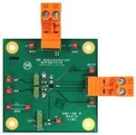
Figure 18. PCB Layout example
ORDERING INFORMATION
Package
Shipping†
WLCSP9
(Pb−Free)
3000 / Tape & Reel
WLCSP9
(Backside Laminate Coating)
(Pb−Free)
3000 / Tape & Reel
NCP2823BFCT1G
WLCSP9
(Pb−Free)
3000 / Tape & Reel
NCP2823BFCT2G
WLCSP9
(Pb−Free)
3000 / Tape & Reel
Device
NCP2823AFCT2G
NCP2823AFCCT2G
†For information on tape and reel specifications, including part orientation and tape sizes, please refer to our Tape and Reel Packaging
Specifications Brochure, BRD8011/D.
Demo Board Available:
NCP2823AGEVB/D and NCP2823BGEVB/D evaluation board configure the device in typical application.
http://onsemi.com
10
�MECHANICAL CASE OUTLINE
PACKAGE DIMENSIONS
9 PIN FLIP−CHIP 1.45x1.45x0.596
CASE 499AL
ISSUE A
DATE 21 JUN 2022
GENERIC
MARKING DIAGRAM*
A3
A1
XXXX
AYWW
C1
XXXX
A
Y
WW
G or G
= Specific Device Code
= Assembly Location
= Year
= Work Week
= Pb−Free Package
*This information is generic. Please refer to
device data sheet for actual part marking.
Pb−Free indicator, “G” or microdot “G”, may
or may not be present. Some products may
not follow the Generic Marking.
DOCUMENT NUMBER:
DESCRIPTION:
98AON19548D
Electronic versions are uncontrolled except when accessed directly from the Document Repository.
Printed versions are uncontrolled except when stamped “CONTROLLED COPY” in red.
9 PIN FLIP−CHIP 1.45x1.45x0.596
PAGE 1 OF 1
onsemi and
are trademarks of Semiconductor Components Industries, LLC dba onsemi or its subsidiaries in the United States and/or other countries. onsemi reserves
the right to make changes without further notice to any products herein. onsemi makes no warranty, representation or guarantee regarding the suitability of its products for any particular
purpose, nor does onsemi assume any liability arising out of the application or use of any product or circuit, and specifically disclaims any and all liability, including without limitation
special, consequential or incidental damages. onsemi does not convey any license under its patent rights nor the rights of others.
© Semiconductor Components Industries, LLC, 2019
www.onsemi.com
�onsemi,
, and other names, marks, and brands are registered and/or common law trademarks of Semiconductor Components Industries, LLC dba “onsemi” or its affiliates
and/or subsidiaries in the United States and/or other countries. onsemi owns the rights to a number of patents, trademarks, copyrights, trade secrets, and other intellectual property.
A listing of onsemi’s product/patent coverage may be accessed at www.onsemi.com/site/pdf/Patent−Marking.pdf. onsemi reserves the right to make changes at any time to any
products or information herein, without notice. The information herein is provided “as−is” and onsemi makes no warranty, representation or guarantee regarding the accuracy of the
information, product features, availability, functionality, or suitability of its products for any particular purpose, nor does onsemi assume any liability arising out of the application or use
of any product or circuit, and specifically disclaims any and all liability, including without limitation special, consequential or incidental damages. Buyer is responsible for its products
and applications using onsemi products, including compliance with all laws, regulations and safety requirements or standards, regardless of any support or applications information
provided by onsemi. “Typical” parameters which may be provided in onsemi data sheets and/or specifications can and do vary in different applications and actual performance may
vary over time. All operating parameters, including “Typicals” must be validated for each customer application by customer’s technical experts. onsemi does not convey any license
under any of its intellectual property rights nor the rights of others. onsemi products are not designed, intended, or authorized for use as a critical component in life support systems
or any FDA Class 3 medical devices or medical devices with a same or similar classification in a foreign jurisdiction or any devices intended for implantation in the human body. Should
Buyer purchase or use onsemi products for any such unintended or unauthorized application, Buyer shall indemnify and hold onsemi and its officers, employees, subsidiaries, affiliates,
and distributors harmless against all claims, costs, damages, and expenses, and reasonable attorney fees arising out of, directly or indirectly, any claim of personal injury or death
associated with such unintended or unauthorized use, even if such claim alleges that onsemi was negligent regarding the design or manufacture of the part. onsemi is an Equal
Opportunity/Affirmative Action Employer. This literature is subject to all applicable copyright laws and is not for resale in any manner.
PUBLICATION ORDERING INFORMATION
LITERATURE FULFILLMENT:
Email Requests to: orderlit@onsemi.com
onsemi Website: www.onsemi.com
◊
TECHNICAL SUPPORT
North American Technical Support:
Voice Mail: 1 800−282−9855 Toll Free USA/Canada
Phone: 011 421 33 790 2910
Europe, Middle East and Africa Technical Support:
Phone: 00421 33 790 2910
For additional information, please contact your local Sales Representative
�