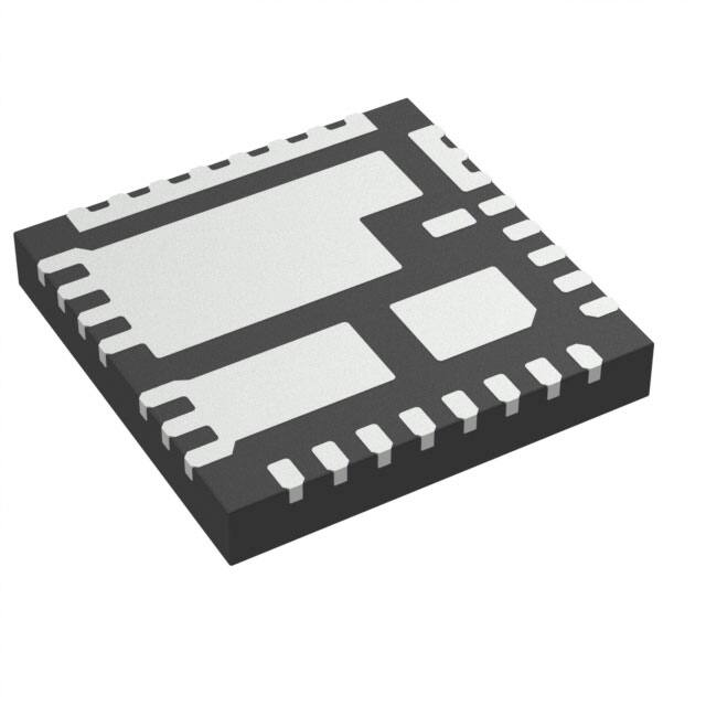
Integrated Driver and
MOSFET
NCP302155
The NCP302155 integrates a MOSFET driver, high−side MOSFET
and low−side MOSFET into a single package.
The driver and MOSFETs have been optimized for high−current
DC−DC buck power conversion applications. The NCP302155
integrated solution greatly reduces package parasitics and board space
compared to a discrete component solution.
www.onsemi.com
Features
Capable of Average Currents up to 55 A
Capable of Switching at Frequencies up to 2 MHz
Compatible with 3.3 V or 5 V PWM Input
Responds Properly to 3−level PWM Inputs
Option for Zero Cross Detection with 3−level PWM
Internal Bootstrap Diode
Undervoltage Lockout
Supports Intel® Power State 4
Thermal Warning output
Thermal Shutdown
PQFN31 5X5, 0.5P
CASE 483BR
MARKING DIAGRAM
NCP
302155
AWLYYWW
Pin1
A
WL
YY
WW
Applications
• Notebook, Tablet PC and Ultrabook
• Servers and Workstations, V−Core and Non−V−Core DC−DC
Converters
VCC
SMOD#
PWM
2
1
32
AGND
11
5V
18
19
20
21
22
DISB#
THWN
VCCD
PGND
GL
VSW
VSW
VSW
23
VSW
17
VSW
16
VSW
PGND
PGND
VSW
VOUT
VSW
CGND
VSW
VSW
SMOD#
VSW
PWM
PGND
VSW
BOOT
15
PWM from controller
SMOD from controller
DISB#
PGND
THWN
14
DRVON from controller
ZCD_EN
13
Zero Current
Detect Enable
VIN
12
PGND
VCCD VCC
33
GL
31
CGND
3
30
BOOT
4
29
nc
5
28
PHASE
6
27
10
VIN
7
26
VIN
8
25
VIN
9
•
•
VIN
PINOUT DIAGRAM
• Desktop and All−in−One Computers, V−Core and Non−V−Core
DC−DC Converters
High−Current DC−DC Point−of−Load Converters
Small Form−Factor Voltage Regulator Modules
= Assembly Location
= Wafer Lot
= Year
= Work Week
24
•
•
•
•
•
•
•
•
•
•
ORDERING INFORMATION
Figure 1. Application Schematic
Device
NCP302155MNTWG
Package
Shipping†
PQFN31
5x5
3000 / Tape &
Reel
†For information on tape and reel specifications,
including part orientation and tape sizes, please
refer to our Tape and Reel Packaging Specifications
Brochure, BRD8011/D.
© Semiconductor Components Industries, LLC, 2018
August, 2021 − Rev. 5
1
Publication Order Number:
NCP302155/D
�NCP302155
VCCD 29
VCC
5 BOOT
3
VCC
SMOD#
2
PWM
1
8−11 VIN
LEVEL
SHIFT
UVLO
16−26 VSW
7 PHASE
DEAD
TIME
CONTROL
SHUTDOWN
TEMP
WARNING SENSE
DISB# 31
LEVEL
SHIF
28 PGND
THWN 30
12−15 PGND
27 GL
AGND 32
CGND
33 GL
ZCD
CONTROL
4
Figure 2. Block Diagram
Table 1. PIN LIST AND DESCRIPTION
Pin No.
Symbol
1
PWM
2
SMOD#
3
VCC
4, 32
CGND, AGND
5
BOOT
6
nc
7
PHASE
8−11
VIN
12−15, 28
PGND
16−26
VSW
Description
PWM Control Input and Zero Current Detection Enable
Skip Mode pin. 3−state input (see Table 6):
SMOD# = High ³ State of PWM determine whether the NCP302155 performs ZCD or not.
SMOD# = Mid ³ Connects PWM to internal resistor divider placing a bias voltage on PWM pin.
Otherwise, logic is equivalent to SMOD# in the high state.
SMOD# = Low ³ Placing PWM into mid−state pulls GH and GL low without delay.
There is an internal pull−up resistor to VCC on this pin.
Control Power Supply Input
Signal Ground (pin 4 and pad 32 are internally connected)
Bootstrap Voltage
Open pin (not used)
Bootstrap Capacitor Return
Conversion Supply Power Input
Power Ground
Switch Node Output
27, 33
GL
29
VCCD
Low Side FET Gate Access (pin 27 and pad 33 are internally connected)
Driver Power Supply Input
30
THWN
Thermal warning indicator. This is an open−drain output. When the temperature at the driver die
reaches TTHWN, this pin is pulled low.
31
DISB#
Output disable pin. When this pin is pulled to a logic high level, the driver is enabled. There is an
internal pull−down resistor on this pin.
www.onsemi.com
2
�NCP302155
Table 2. ABSOLUTE MAXIMUM RATINGS (Electrical Information − all signals referenced to PGND unless noted otherwise)
Min
Max
Unit
VCC, VCCD
−0.3
6.5
V
VIN
−0.3
30
V
BOOT (DC)
−0.3
35
V
BOOT (< 20 ns)
−0.3
40
V
BOOT to PHASE (DC)
−0.3
6.5
V
VSW, PHASE (DC)
−0.3
30
V
VSW, PHASE (< 20 ns)
−5
35
V
PHASE (< 5 ns)
−15
35
V
All Other Pins
−0.3
VVCC + 0.3
V
Pin Name / Parameter
Stresses exceeding those listed in the Maximum Ratings table may damage the device. If any of these limits are exceeded, device functionality
should not be assumed, damage may occur and reliability may be affected.
Table 3. THERMAL INFORMATION
Rating
Symbol
Value
Unit
qJA
12.4
_C/W
qJ−PCB
1.8
_C/W
Operating Junction Temperature Range (Note 1)
TJ
−40 to +150
_C
Operating Ambient Temperature Range
TA
−40 to +125
_C
Maximum Storage Temperature Range
TSTG
−55 to +150
_C
10.5
W
Thermal Resistance (under On Semi SPS Thermal Board)
Maximum Power Dissipation
Moisture Sensitivity Level
MSL
1
1. The maximum package power dissipation must be observed.
2. JESD 51−5 (1S2P Direct−Attach Method) with 0 LFM
3. JESD 51−7 (1S2P Direct−Attach Method) with 0 LFM
Table 4. RECOMMENDED OPERATING CONDITIONS
Parameter
Supply Voltage Range
Conversion Voltage
Continuous Output Current
Peak Output Current
Pin Name
Conditions
Min
Typ
Max
Unit
VCC, VCCD
4.5
5.0
5.5
V
VIN
4.5
19
24
V
FSW = 1 MHz, VIN = 12 V, VOUT = 1.0 V, TA = 25_C
55
A
FSW = 300 kHz, VIN = 12 V, VOUT = 1.0 V, TA = 25_C
60
A
Duration = 5 ms, Period = 10 ms
85
A
FSW = 500 kHz, VIN = 12 V, VOUT = 1.0 V,
Duration = 10 ms, Period = 1 s, TA = 25_C
80
A
125
_C
Junction Temperature
−40
Functional operation above the stresses listed in the Recommended Operating Ranges is not implied. Extended exposure to stresses beyond
the Recommended Operating Ranges limits may affect device reliability.
www.onsemi.com
3
�NCP302155
Table 5. ELECTRICAL CHARACTERISTICS
(VVCC = VVCCD = 5.0 V, VVIN = 12 V, VDISB# = 2.0 V, CVCCD = CVCC = 0.1 mF unless specified otherwise) Min/Max values are valid for the
temperature range −40°C ≤ TJ ≤ 125°C unless noted otherwise, and are guaranteed by test, design or statistical correlation.)
Parameter
Symbol
Conditions
Min.
Typ.
Max.
Unit
1
2
mA
VCC SUPPLY CURRENT
Operating
DISB# = 5 V, PWM = 400 kHz
−
No switching
DISB# = 5 V, PWM = 0 V
−
−
2
mA
Disabled
DISB# = 0 V, SMOD# = VCC
−
0.4
1
mA
6
15
mA
2.89
−
3.37
V
150
−
−
mV
DISB# = 0 V, SMOD# = GND
UVLO Start Threshold
VUVLO
VCC rising
UVLO Hysteresis
VCCD SUPPLY CURRENT
Enabled, No switching
DISB# = 5 V, PWM = 0 V,
VPHASED = 0 V
−
175
300
mA
Disabled
DISB# = 0 V
−
0.4
1
mA
Operating
DISB# = 5 V, PWM = 400 kHz
−
−
26
mA
To Ground
−
467
−
kW
DISB# INPUT
Input Resistance
Upper Threshold
VUPPER
−
−
2.0
V
Lower Threshold
VLOWER
0.8
−
−
V
200
−
−
mV
Hysteresis
VUPPER − VLOWER
Enable Delay Time
Time from DISB# transitioning HI
to when VSW responds to PWM.
−
−
40
ms
Disable Delay Time
Time from DISB# transitioning
LOW to when both output FETs
are off.
−
21
50
ns
SMOD# INPUT
SMOD# Input Voltage High
VSMOD_HI
2.65
−
−
V
SMOD# Input Voltage Mid−state
VSMOD#_MID
1.4
−
2.0
V
SMOD# Input Voltage Low
VSMOD_LO
−
−
0.7
V
SMOD# Input Resistance
RSMOD#_UP
Pull−up resistance to VCC
−
455
−
kW
SMOD# Propagation Delay, Falling
TSMOD#_PD_F
SMOD# = Low to GL = 90%,
PWM = MID
−
34
42
ns
SMOD# Propagation Delay, Rising
TSMOD#_PD_R
SMOD# = High to GL = 10%,
PWM = MID
−
22
30
ns
PWM INPUT
Input Voltage High
VPWM_HI
2.65
−
−
V
Input Mid−state Voltage
VPWM_MID
1.4
−
2.1
V
Input Low Voltage
VPWM_LO
−
−
0.7
V
Input Resistance
RPWM_HIZ
SMOD# = VSMOD#_HI or
VSMOD#_LO
10
−
−
MW
Input Resistance
RPWM_BIAS
SMOD# = VSMOD#_MID
−
68
−
kW
PWM Input Bias Voltage
VPWM_BIAS
SMOD# = VSMOD#_MID
−
1.7
−
V
Non−overlap Delay, Leading Edge
TNOL_L
GL Falling = 1 V to GH−VSW Rising = 1 V
−
13
−
ns
Non−overlap Delay, Trailing Edge
TNOL_T
GH−VSW Falling = 1 V to
GL Rising = 1 V
−
12
−
ns
PWM Propagation Delay, Rising
TPWM,PD_R
PWM = High to GL = 90%
−
13
35
ns
www.onsemi.com
4
�NCP302155
Table 5. ELECTRICAL CHARACTERISTICS
(VVCC = VVCCD = 5.0 V, VVIN = 12 V, VDISB# = 2.0 V, CVCCD = CVCC = 0.1 mF unless specified otherwise) Min/Max values are valid for the
temperature range −40°C ≤ TJ ≤ 125°C unless noted otherwise, and are guaranteed by test, design or statistical correlation.)
Parameter
Symbol
Conditions
Min.
Typ.
Max.
Unit
PWM Propagation Delay, Falling
TPWM,PD_F
PWM = Low to SW = 90%
−
47
52
ns
Exiting PWM Mid−state Propagation
Delay, Mid−to−Low
TPWM_EXIT_L
PWM = Mid−to−Low to GL = 10%
−
14
25
ns
Exiting PWM Mid−state Propagation
Delay, Mid−to−High
TPWM_EXIT_H
PWM = Mid−to−High to SW = 10%
−
13
25
ns
ZD FUNCTION
Zero Cross Detect Threshold
VZCD
−
−6
−
mV
ZCD Blanking + Debounce Time
tBLNK
−
330
−
ns
−
150
−
_C
−
15
−
_C
−
180
−
_C
THERMAL WARNING & SHUTDOWN
Thermal Warning Temperature
TTHWN
Thermal Warning Hysteresis
TTHWN_HYS
Temperature at Driver Die
Thermal Shutdown Temperature
TTHDN
Thermal Shutdown Hysteresis
TTHDN_HYS
−
25
−
_C
THWM Open Drain Current
ITHWN
−
−
5
mA
Forward Bias Current = 2.0 mA
−
380
−
mV
Source Current = 100 mA
−
0.9
−
W
−
2
−
A
−
0.7
−
W
−
2.5
−
A
Temperature at Driver Die
BOOST STRAP DIODE
Forward Voltage
HIGH−SIDE DRIVER
Output Impedance, Sourcing
RSOURCE_GH
Output Sourcing Peak Current
ISOURCE_GH
Output Impedance, Sinking
RSINK_GH
Output Sinking Peak Current
ISINK_GH
Source Current = 100 mA
LOW−SIDE DRIVER
Output Impedance, Sourcing
RSOURCE_GL
Source Current = 100 mA
−
0.9
−
W
Output Sourcing Peak Current
ISOURCE_GL
GL = 2.5 V
−
2
−
A
Output Impedance, Sinking
RSINK_GH
Sink Current = 100 mA
−
0.4
−
W
Output Sinking Peak Current
ISINK_GL
GL = 2.5 V
−
4.5
−
A
GL Rise Time
TR_GL
GL = 10% to 90%, CLOAD = 3.0 nF
−
12
−
ns
GL Fall Time
TF_GL
GL = 90% to 10%, CLOAD = 3.0 nF
−
6
−
ns
Product parametric performance is indicated in the Electrical Characteristics for the listed test conditions, unless otherwise noted. Product
performance may not be indicated by the Electrical Characteristics if operated under different conditions.
www.onsemi.com
5
�NCP302155
Table 6. LOGIC TABLE
INPUT TRUTH TABLE
DISB#
PWM
SMOD# (Note 4)
GH (not a pin)
GL
L
X
X
L
L
H
H
X
H
L
H
L
X
L
H
H
MID
H or MID
L
ZCD (Note 5)
H
MID
L
L
L (Note 6)
4. PWM input is driven to mid−state with internal divider resistors when SMOD# is driven to mid−state and PWM input is undriven externally.
5. GL goes low following 80 ns de−bounce time, 250 ns blanking time and then SW exceeding ZCD threshold.
6. There is no delay before GL goes low.
www.onsemi.com
6
�NCP302155
TYPICAL PERFORMANCE CHARACTERISTICS
Test Conditions: VIN = 12 V, VCC = VCCD = 5 V, VOUT = 1 V, LOUT = 250 nH, TA = 25 °C and natural convection cooling, unless
otherwise noted.
Figure 3. Efficiency − 19 V Input, 1.0 V Output
Figure 4. Efficiency − 19 V Input, 1.8 V Output
Figure 5. Efficiency − 12 V Input, 1.0 V Output
Figure 6. Efficiency − 12 V Input, 1.8 V Output
Figure 7. Power Iosses vs. Output Current, 12 Vin
Figure 8. Power Iosses vs. Output Current, 19 Vin
www.onsemi.com
7
�NCP302155
TYPICAL PERFORMANCE CHARACTERISTICS
Test Conditions: VIN = 12 V, VCC = PVCC = 5 V, VOUT = 1 V, LOUT = 250 nH, TA = 25 °C and natural convection cooling, unless
otherwise noted.
Figure 9. Power Loss vs. Switching Frequency
Figure 10. Power Loss vs. Input Voltage
Figure 11. Power Loss vs. Driver Supply Voltage
Figure 12. Power Loss vs. Output Voltage
Figure 13. Driver Supply Current vs. Switching
Frequency
Figure 14. Driver Supply Current vs. Driver Supply
Voltage
www.onsemi.com
8
�NCP302155
Theory of Operation
Safety Timer and Overlap Protection Circuit
The NCP302155 is an integrated driver and MOSFET
module designed for use in a synchronous buck converter
topology. The NCP302155 supports numerous application
control definitions including ZCD (Zero Current Detect)
and alternately PWM Tristate control. A PWM input signal
is required to control the drive signals to the high−side and
low−side integrated MOSFETs.
It is important to avoid cross−conduction of the two
MOSFETS which could result in a decrease in the power
conversion efficiency or damage to the device.
The NCP302155 prevents cross−conduction by
monitoring the status of the MOSFETs and applying the
appropriate amount of non−overlap (NOL) time (the time
between the turn−off of one MOSFET and the turn−on of the
other MOSFET). When the PWM input pin is driven high,
the gate of the low−side MOSFET (LSGATE) goes low after
a propagation delay (tpdlGL). The time it takes for the
low−side MOSFET to turn off is dependent on the total
charge on the low−side MOSFET gate.
The NCP302155 monitors the gate voltage of both
MOSFETs and the switch node voltage to determine the
conduction status of the MOSFETs. Once the low−side
MOSFET is turned off an internal timer delays (tpdhGH) the
turn−on of the high−side MOSFET. When the PWM input
pin goes low, the gate of the high−side MOSFET (HSGATE)
goes low after the propagation delay (tpdlGH). The time to
turn off the high−side MOSFET (tfGH) is dependent on the
total gate charge of the high−side MOSFET. A timer is
triggered once the high−side MOSFET stops conducting, to
delay (tpdhGL) the turn−on of the low−side MOSFET.
Low−Side Driver
The
low−side
driver
drives
an
internal,
ground−referenced low−RDS(on) N−Channel MOSFET.
The voltage supply for the low−side driver is internally
connected to the VCCD and PGND pins.
High−Side Driver
The high−side driver drives an internal, floating
low−RDS(on) N−channel MOSFET. The gate voltage for the
high side driver is developed by a bootstrap circuit
referenced to Switch Node (VSW and PHASE) pins.
The bootstrap circuit is comprised of the integrated diode
and an external bootstrap capacitor and resistor. When the
NCP302155 is starting up, the VSW pin is at ground,
allowing the bootstrap capacitor to charge up to VCCD
through the bootstrap diode (See Figure 1). When the PWM
input is driven high, the high−side driver turns on the
high−side MOSFET using the stored charge of the bootstrap
capacitor. As the high−side MOSFET turns on, the voltage
at the VSW and PHASE pins rises. When the high−side
MOSFET is fully turned on, the switch node settles to VIN
and the BST pin settles to VIN + VCCD (excluding parasitic
ringing).
Zero Current Detect
The bootstrap circuit relies on an external charge storage
capacitor (CBST) and an integrated diode to provide current
to the HS Driver. A multi−layer ceramic capacitor (MLCC)
with a value greater than 100 nF should be used as the
bootstrap capacitor. An optional 1 to 4 W resistor in series
with the bootstrap capacitor decreases the VSW overshoot.
The Zero Current Detect PWM (ZCD_PWM) mode is
enabled when SMOD# is high (see tables 6 and 8).
With PWM set to > VPWM_HI, GL goes low and GH
goes high after the non−overlap delay. When PWM is driven
to < VPWM_HI and to > VPWM_LO, GL goes high after
the non−overlap delay, and stays high for the duration of the
ZCD blanking timer (TZCD_BLANK) and an 80 ns de−bounce
timer. Once this timer expires, VSW is monitored for zero
current detection, and GL is pulled low once zero current is
detected. The threshold on VSW to determine zero current
undergoes an auto−calibration cycle every time DISB# is
brought from low to high. This auto−calibration cycle
typically takes 25 ms to complete.
Power Supply Decoupling
PWM Input
Bootstrap Circuit
The PWM Input pin is a tri−state input used to control the
HS MOSFET ON/OFF state. It also determines the state of
the LS MOSFET. See Table 6 for logic operation. The PWM
in some cases must operate with frequency programming
resistances to ground. These resistances can range from
10 kW to 300 kW depending on the application. When
SMOD# is set to > VSMOD#_HI or to < VSMOD#_LO, the
input impedance to the PWM input is very high in order to
avoid interferences with controllers that must use
programming resistances on the PWM pin.
If SMOD# is set to < VSMOD#_HI and > VSMOD#_LO
(Mid−State), the PWM pin undriven default voltage is set to
Mid−State with internal divider resistances.
The NCP302155 sources relatively large currents into the
MOSFET gates. In order to maintain a constant and stable
supply voltage (VCCD) a low−ESR capacitor should be
placed near the power and ground pins. A multi−layer
ceramic capacitor (MLCC) between 1 mF and 4.7 mF is
typically used.
A separate supply pin (VCC) is used to power the analog
and digital circuits within the driver. A 1 mF ceramic
capacitor should be placed on this pin in close proximity to
the NCP302155. It is good practice to separate the VCC and
VCCD decoupling capacitors with a resistor (10 W typical)
to avoid coupling driver noise to the analog and digital
circuits that control the driver function (See Figure 1).
www.onsemi.com
9
�NCP302155
Disable Input (DISB#)
VCC Undervoltage Lockout
The DISB# pin is used to disable the GH to the High−Side
FET to prevent power transfer. The pin has a pull−down
resistance to force a disabled state when it is left
unconnected. DISB# can be driven from the output of a logic
device or set high with a pull−up resistance to VCC.
The VCC pin is monitored by an Undervoltage Lockout
Circuit (UVLO). VCC voltage above the rising threshold
enables the NCP302155.
Table 7. Table 2. UVLO/DISB# LOGIC TABLE
UVLO
L
H
H
H
DISB#
X
L
H
Open
Driver State
Disabled (GH = GL = 0)
Disabled (GH = GL = 0)
Enabled (See Table 1)
Disabled (GH = GL = 0)
Thermal Warning/Thermal Shutdown Output
enables the low side synchronous MOSFET to operate
independently of the internal ZCD function. When the
SMOD# pin is set low during the PWM cycle it disables the
low side MOSFET to allow discontinuous mode operation.
The NCP302155 has the capability of internally
connecting a resistor divider to the PWM pin. To engage this
mode, SMOD# needs to be placed into mid−state. While in
SMOD# mid−state, the IC logic is equivalent to SMOD#
being in the high state.
The THWN pin is an open drain output. When the
temperature of the driver exceeds TTHWN, the THWN pin is
pulled low indicating a thermal warning. At this point, the
part continues to function normally. When the temperature
drops TTHWN_HYS below TTHWN, the THWN pin goes high. If
the driver temperature exceeds TTHDN, the part enters
thermal shutdown and turns off both MOSFETs. Once the
temperature falls TTHDN_HYS below TTHDN, the part resumes
normal operation.
Skip Mode Input (SMOD#)
The SMOD# tri−state input pin has an internal pull−up
resistance to VCC. When driven high, the SMOD# pin
NOTE: If the Zero Current Detect circuit detects zero current after the ZCD Wait timer period, the GL is driven low by
the Zero Current Detect signal.
If the Zero Current Detect circuit detects zero current before the ZCD Wait timer period expires, the Zero Current
detect signal is ignored and the GL is driven low at the end of the ZCD Wait timer period.
NOTE: If the SMOD# input is driven low at any time after the GL has been driven high, the SMOD# Falling edge
triggers the GL to go low.
If the SMOD# input is driven low while the GH is high, the SMOD# input is ignored.
www.onsemi.com
10
�NCP302155
Inductor
Current
PWM
GH
SMOD#
triggered
GL
SMOD#
Figure 15. SMOD# Timing Diagram
NOTE: If the SMOD# input is driven low at any time after the GL has been driven high, the SMOD# Falling edge
triggers the GL to go low.
If the SMOD# input is driven low while the GH is high, the SMOD# input is ignored.
For Use with Controllers with 3−State PWM and No
Zero Current Detection Capability:
Table 8. LOGIC TABLE − 3−STATE PWM CONTROLLERS WITH NO ZCD
PWM
SMOD#
GH (not a pin)
GL
H
H
ON
OFF
M
H
OFF
ZCD
L
H
OFF
ON
and low states. To enter into DCM, PWM needs to be
switched to the mid−state.
Whenever PWM transitions to mid−state, GH turns off
and GL turns on. GL stays on for the duration of the
de−bounce timer and ZCD blanking timers. Once these
timers expire, the NCP302155 monitors the SW voltage and
turns GL off when SW exceeds the ZCD threshold voltage.
By turning off the LS FET, the body diode of the LS FET
allows any positive current to go to zero but prevents
negative current from conducting.
This section describes operation with controllers that are
capable of 3 states in their PWM output and relies on the
NCP302155 to conduct zero current detection during
discontinuous conduction mode (DCM).
The SMOD# pin needs to either be set to 5 V or left
disconnected. The NCP302155 has an internal pull−up
resistor that connects to VCC that sets SMOD# to the logic
high state if this pin is disconnected.
To operate the buck converter in continuous conduction
mode (CCM), PWM needs to switch between the logic high
www.onsemi.com
11
�NCP302155
Figure 16. Timing Diagram − 3−state PWM Controller, No ZCD
FOR USE WITH CONTROLLERS WITH 3−STATE
PWM CONTROLLERS DETECTION CAPABILITY:
Table 9. LOGIC TABLE − 3−STATE PWM CONTROLLERS WITH ZCD
PWM
SMOD#
GH (not a pin)
GL
H
L
ON
OFF
M
L
OFF
OFF
L
L
OFF
ON
This section describes operation with controllers that are
capable of 3 PWM output levels and have zero current
detection during discontinuous conduction mode (DCM).
The SMOD# pin needs to be pulled low (below
and low states. During DCM, the controller is responsible
for detecting when zero current has occurred, and then
notifying the NCP302155 to turn off the LS FET. When the
controller detects zero current, it needs to set PWM to
mid−state, which causes the NCP302155 to pull both GH
and GL to their off states without delay.
VSMOD#_LO).
To operate the buck converter in continuous conduction
mode (CCM), PWM needs to switch between the logic high
www.onsemi.com
12
�NCP302155
SMOD# 0 V
SMOD# = Low
IL 0 A
Controller detects zero current →
Sets
PWM to mid−state.
PWM
PWM in mid−state pulls GL
low.
GH
GL
Figure 17. Timing Diagram − 3−state PWM Controller, with ZCD
Figure 18. Top Copper Layer
www.onsemi.com
13
�NCP302155
Figure 19. Bottom Copper Layer
www.onsemi.com
14
�NCP302155
RECOMMENDED PCB FOOTPRINT
(Option 1)
LAND PATTERN
RECOMMENDATION
RECOMMENDED MOUNTING FOOTPRINT
For additional information on our Pb-Free strategy and soldering
details, please download the ON Semiconductor Soldering and
Mounting Techniques Reference Manual, SOLDERRM/D.
www.onsemi.com
15
�NCP302155
RECOMMENDED PCB FOOTPRINT
(Option 2)
LAND PATTERN
RECOMMENDATION
RECOMMENDED MOUNTING FOOTPRINT
For additional information on our Pb-Free strategy and soldering
details, please download the ON Semiconductor Soldering and
Mounting Techniques Reference Manual, SOLDERRM/D.
www.onsemi.com
16
�MECHANICAL CASE OUTLINE
PACKAGE DIMENSIONS
PQFN31 5X5, 0.5P
CASE 483BR
ISSUE A
DATE 24 APR 2020
SCALE 2.5:1
GENERIC
MARKING DIAGRAM*
XXXXXXXX
XXXXXXXX
AWLYYWWG
G
DOCUMENT NUMBER:
DESCRIPTION:
XXXX
A
WL
YY
WW
G
= Specific Device Code
= Assembly Location
= Wafer Lot
= Year
= Work Week
= Pb−Free Package
(Note: Microdot may be in either location)
98AON13680G
PQFN31 5X5, 0.5P
*This information is generic. Please refer to
device data sheet for actual part marking.
Pb−Free indicator, “G” or microdot “G”, may
or may not be present. Some products may
not follow the Generic Marking.
Electronic versions are uncontrolled except when accessed directly from the Document Repository.
Printed versions are uncontrolled except when stamped “CONTROLLED COPY” in red.
PAGE 1 OF 1
ON Semiconductor and
are trademarks of Semiconductor Components Industries, LLC dba ON Semiconductor or its subsidiaries in the United States and/or other countries.
ON Semiconductor reserves the right to make changes without further notice to any products herein. ON Semiconductor makes no warranty, representation or guarantee regarding
the suitability of its products for any particular purpose, nor does ON Semiconductor assume any liability arising out of the application or use of any product or circuit, and specifically
disclaims any and all liability, including without limitation special, consequential or incidental damages. ON Semiconductor does not convey any license under its patent rights nor the
rights of others.
© Semiconductor Components Industries, LLC, 2018
www.onsemi.com
�onsemi,
, and other names, marks, and brands are registered and/or common law trademarks of Semiconductor Components Industries, LLC dba “onsemi” or its affiliates
and/or subsidiaries in the United States and/or other countries. onsemi owns the rights to a number of patents, trademarks, copyrights, trade secrets, and other intellectual property.
A listing of onsemi’s product/patent coverage may be accessed at www.onsemi.com/site/pdf/Patent−Marking.pdf. onsemi reserves the right to make changes at any time to any
products or information herein, without notice. The information herein is provided “as−is” and onsemi makes no warranty, representation or guarantee regarding the accuracy of the
information, product features, availability, functionality, or suitability of its products for any particular purpose, nor does onsemi assume any liability arising out of the application or use
of any product or circuit, and specifically disclaims any and all liability, including without limitation special, consequential or incidental damages. Buyer is responsible for its products
and applications using onsemi products, including compliance with all laws, regulations and safety requirements or standards, regardless of any support or applications information
provided by onsemi. “Typical” parameters which may be provided in onsemi data sheets and/or specifications can and do vary in different applications and actual performance may
vary over time. All operating parameters, including “Typicals” must be validated for each customer application by customer’s technical experts. onsemi does not convey any license
under any of its intellectual property rights nor the rights of others. onsemi products are not designed, intended, or authorized for use as a critical component in life support systems
or any FDA Class 3 medical devices or medical devices with a same or similar classification in a foreign jurisdiction or any devices intended for implantation in the human body. Should
Buyer purchase or use onsemi products for any such unintended or unauthorized application, Buyer shall indemnify and hold onsemi and its officers, employees, subsidiaries, affiliates,
and distributors harmless against all claims, costs, damages, and expenses, and reasonable attorney fees arising out of, directly or indirectly, any claim of personal injury or death
associated with such unintended or unauthorized use, even if such claim alleges that onsemi was negligent regarding the design or manufacture of the part. onsemi is an Equal
Opportunity/Affirmative Action Employer. This literature is subject to all applicable copyright laws and is not for resale in any manner.
PUBLICATION ORDERING INFORMATION
LITERATURE FULFILLMENT:
Email Requests to: orderlit@onsemi.com
onsemi Website: www.onsemi.com
◊
TECHNICAL SUPPORT
North American Technical Support:
Voice Mail: 1 800−282−9855 Toll Free USA/Canada
Phone: 011 421 33 790 2910
Europe, Middle East and Africa Technical Support:
Phone: 00421 33 790 2910
For additional information, please contact your local Sales Representative
�