NCP30653ABCKGEVB,
NCP3065SOBCKGEVB,
NCP3065SOBSTGEVB
High Intensity LED Drivers
Using NCP3065/NCV3065
Evaluation Board User's
Manual
Introduction
http://onsemi.com
EVAL BOARD USER’S MANUAL
High brightness LEDs are a prominent source of light and
have better efficiency and reliability than conventional light
sources. Improvements in high brightness LEDs present the
potential for creative new lighting solutions that offer an
improved lighting experience while reducing energy
demand. LEDs require constant current driver solutions due
to their wide forward voltage variation and steep V/I transfer
function. For applications that are powered from low
voltage AC sources typically used in landscape lighting or
low voltage DC sources that may be used in automotive
applications, high efficiency driver that can operate over
wide range of input voltages to drive series strings of one to
several LEDs.
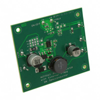
Figure 1. NCP3065 3A Buck Evaluation Board
Figure 2. NCP3065 Buck Evaluation Board
NCP3065/NCV3065 EVALUATION BOARD
NCP3065/NCV3065 can operate as a switcher or as a
controller. These options are shown bellow.
The brightness of the LEDs or light intensity is measured
in Lumens and is proportional to the forward current flowing
through the LED. The light efficiency can vary with the
current flowing through the LED string.
The NCP3065 is rated for commercial/industrial
temperature ranges and the NCV3065 is automotive
qualified.
This evaluation board user’s manual describes a DC−DC
converter circuits that can easily be configured to drive
LEDs at several different output currents and can be
configured for either AC or DC input. The
NCP3065/NCV3065 can be configured in a several driver
topologies to a drive string of LEDs: be it traditional low
power LEDs or high brightness high power LEDs such as the
Lumileds Luxeon K2 and Rebel series, the CREE
XLAMP 4550 or XR series, the OSRAM OSTAR,
TopLED and Golden Dragon. Configurations like this
are found in 12 VDC track lighting applications, automotive
applications, and low voltage AC landscaping applications
as well as track lighting such as under-cabinet lights and
desk lamps that might be powered from standard
off-the-shelf 5 VDC and 12 VDC wall adapters. The
Semiconductor Components Industries, LLC, 2012
November, 2012 − Rev. 1
Evaluation Board Design Versions
The evaluation boards are designed to display the full
functionality and flexibility of NCP3065 as a driver to drive
various LEDs at the low voltage AC and DC sources. The
components are selected for the 15 W LED driver
1
Publication Order Number:
EVBUM2155/D
�NCP30653ABCKGEVB, NCP3065SOBCKGEVB, NCP3065SOBSTGEVB
solutions. Each application is described by the schematic
and the bill of material and it has the option of LED dimming
by using an external PWM signal.
application. Based on this circuit, there are many possible
configurations with different input voltages and output
power levels that could be derived by making some minor
components changes. Table 1 shows these different circuit
Table 1. COMPONENTS CHANGES FOR DIFFERENT CONFIGURATIONS
LED Driver
VIN
ILED
VF
L
COUT
R8
Application
(V)
(mA)
(V)
(mH)
(mF)
(W)
12 VDC 1 W LED
10 − 14
350
3.6
47
150
100
0
12k
3k3
12 VDC 3 W LED
10 − 14
700 or 350
3.6 or 7.2
47
150
100
0
16k
12k
12 VDC 5 W LED
10 − 14
700 or 1,000
7.2 or 3.6
47
150
100
0
12k
12k
24 VDC 5 W LED
21 − 27
350
14
68
220
100
0
160k
39k
24 VDC 10 W LED
21 − 27
700
14
68
220
100
0
150k
100k
12 VAC 1 W LED
14 − 20
350
3.6
47
220
100
0
7k5
7k5
12 VAC 3 W LED
14 − 20
700 or 350
3.6 or 7.2
47
220
100
0
22k
22k
12 VAC 5 W LED
14 − 20
700 or 1,000
7.2 or 3.6
47
220
100
0
36k
100k/16k
12 VAC 5 W
14 − 20
350
14
47
220
100
0
NU
NU
12 VAC 15 W
21 − 27
1,000
14
47
100
82k
BUCK
COMPONENT SELECTION
Inductor
ripple current specification to allow higher peak to peak
values. This is achieved by configuring the NCP3065 in a
continuous conduction buck configuration with low peak to
peak ripple thus eliminating the need for an output filter
capacitor. The important design parameter is to keep the
peak current below the maximum current rating of the LED.
Using 15% peak-to-peak ripple results in a good
compromise between achieving max average output current
without exceeding the maximum limit. This saves space and
reduces part count for applications that require a compact
footprint. For the common LED currents such as the
350 mA, 700 mA, 1,000 mA we setup inductor ripple
current to the 52.5 mA, 105 mA, 150 mA. With respect
these requirements we are able to select inductor value
(Equation 1).
When selecting an inductor there is a trade off between
inductor size and peak current. In normal applications the
ripple current can range from 15% to 100%. The trade off
being that with small ripple current the inductance value
increases. The advantage is that you can maximize the
current out of the switching regulator.
With Output Capacitor Operation
A traditional buck topology includes an inductor followed
by an output capacitor which filters the ripple. The capacitor
is placed in parallel with the LED or array of LEDs to lower
LED ripple current. With this approach the output
inductance can be reduced which makes the inductance
smaller and less expensive. Alternatively, the circuit could
be run at lower frequency with the same inductor value
which improves the efficiency and expands the output
voltage range. Equation 2 is used to calculate the capacitor
size based on the amount of LED ripple.
L+
V IN * V OUT
DI MAX
T ON
(eq. 1)
Output Capacitor
No Output Capacitor Operation
When you choose output capacitor we have to think about
its value, ESR and ripple current.
A constant current buck regulator such as the NCP3065
focuses on the control of the current through the load, not the
voltage across it. The switching frequency of the NCP3065
is in the range of 100 kHz − 300 kHz which is much higher
than the human eye can detect. This allows us to relax the
C OUT +
http://onsemi.com
2
V IN * (1 * D) * D
DI
+
DV * 8 * f
8 * L * f 2 * DV OUT
(eq. 2)
�NCP30653ABCKGEVB, NCP3065SOBCKGEVB, NCP3065SOBSTGEVB
Current Feedback Loop
the NCP3065 with dimming you can see in Figures 17
and 18 and dimming linearity in the Figure 19. As you can
see in these figures there aren’t any delays in the rise or fall
edges, which give us the required dimming linearity.
To drive LEDs in a constant current mode, the feedback
for the regulator is taken by sensing the voltage drop across
the sensing resistor R12, see Figures 3 or 9. The RC circuit
(R10 & C5) between the sense resistor and the feedback pin
improves converter transient response. The low feedback
reference voltage of 235 mV allows the use of low power
and lower cost sense resistor. Equation 3 calculates the sense
resistor value.
I OUT +
LED Current
(mA)
V REF
R sense
+
0.235 V
R sense
[A ]
NCP3065
+VIN
(eq. 3)
350
680
1/4W
700
330
1/4W
1000
220
1/4W
Comp
GND
IPK
0R10
VCC
C2
GND
COMP
J5
R11
ON/OFF 1k2
Q2
BC817−LT1G
R9
10k
Vout
NCP3065
+
J3
Sensing Resistor Value
(mW)
NC
R1
J2
R10
1k
0805
R12
Rsense 1%
Figure 4. NCP3065 Dimming Solution A
I = 350 mA
700 mA, 1000 mA
NCP3065
Rsense
J2
+VIN
+
NC
R1
R9
0R10
10k
VCC
C2
J3
GND
Figure 3. NCP3065 Current Feedback
COMP
J5
Dimming Possibility
R11
Q2
BC817−LT1G
ON/OFF 1k2
The emitted LED light is proportional to average output
(LED) current. The NCP3065 is capable of analog and
digital PWM dimming. For the dimming we have three
possibilities how to create it. We basically use a PWM signal
with variable duty cycle for the managing output current
value. The COMP or IPK pin of the NCP3065 is used to
provide dimming capability. In digital input mode the PWM
input signal inhibits switching of the regulator and reducing
the average current through the LEDs. In analog input mode
a PWM input signal is RC filtered and the resulting voltage
is summed with the feedback voltage thus reduces the
average current through the LEDs Figure 6. The component
value of the RC filter are dependent on the PWM frequency.
Due to this, the frequency has to be higher. Figure 19
illustrates the linearity of the digital dimming function with
a 200 Hz digital PWM. The dimming frequency range for
digital input mode is basically from 200 Hz to 1 kHz. For
frequencies below 200 Hz the human eye will see the flicker.
The low dimming frequencies are EMI convenient and an
impact to it is small.
The Figure 4 shows us an example of solution A, which
uses the COMP pin to perform the dimming function and
Figure 5 show us an example of solution B. The behavior of
IPK
R10
1k
0805
R12
Rsense 1%
Figure 5. NCP3065 Dimming Solution B
NCP3065
R1
J2
+VIN
0R10
+
IPK
VCC
C2
J3
NC
GND
COMP
J5
R11
ON/OFF
R19
1k
C9
R10
1k
0805
J5
LED
R12
Rsense 1%
Figure 6. NCP3065 Dimming Solution C
http://onsemi.com
3
�NCP30653ABCKGEVB, NCP3065SOBCKGEVB, NCP3065SOBSTGEVB
BOARD LAYOUT
The layout of the evaluation board and schematic is shown
below in Figure 7 and Figure7.
Figure 7. Evaluation Board Layout Top (Not in Scale)
Figure 8. Evaluation Board Silk Screen Top
http://onsemi.com
4
�5
http://onsemi.com
R11
Figure 9. NCP3065 3A Buck Evaluation Board Schematic
R11
ON/OFF 1k2
0805
J6
ON/OFF 1k2
0805
J6
+VAUX
J4
GND
J3
+VIN
J2 0R04
R1
R3 R4
R5
R6
R7
220 mF/50 V
0.1mF
Q1
BC807−LT1G
C2
+
C4
+
C7
C8
IPK
NC
SWC
SWE
1k
C5
6k8
R13
NU
1k
0805
100pF
1.8nF
C3
10k
0805
CT
R8
MMSD4148T1G
D2
R10
R14
NU
NCP3065
SOIC8
VCC TCAP
COMP COMP
GND
VCC
IPK
NC
U1
R15
R9
Q2
BC817−LT1G
1mF/50V 0.1mF
1206 12061206 1206 1206 1206
R2
6 1R0 1%R
Q5
MMBT3904LT1G
Q4
MTB30P06VT4G
R16
0R15 1%
0.1mF
1206
C1
R12
0R15 1%
D1
MBRS540LT3G
DO5040H−223MLB
L1
+
GND
J7
−LED
J5
C6
220 mF/50 V
+LED
J1
NCP30653ABCKGEVB, NCP3065SOBCKGEVB, NCP3065SOBSTGEVB
�6
http://onsemi.com
Figure 10. NCP3065 Buck Evaluation Board Schematic
R11
R11
ON/OFF 1k2
J6
ON/OFF 1k2
J6
+VAUX
J4
GND
J3
+VIN
J2
R3 R4
R5
R6
R7
220mF/50V
0.1mF
Q1
IPK
NC
SWC
SWE
1k
C5
R13
NU
1k
0805
100pF
1.8nF
C3
15k
10k
CT
R8
MMSD4148
D2
R10
R14
NU
NCP3065
SOIC8
VCC TCAP
COMP COMP
GND
VCC
IPK
NC
U1
R9
Q2
BC817−LT1G
C2
+
C4
1206 12061206 1206 1206 1206
R2
BC807−LGT1G
0R10
R1
6x 1R0 $1%R
R15
Q5
MMBT3904LT1G
Q4
NTF2955T1G
C1
R12
Rsense $1%
MBRS140LT3G 0.1mF
1206
D1
L1
GND
J7
−LED
J5
+LED
C6
NU
+
J1
NCP30653ABCKGEVB, NCP3065SOBCKGEVB, NCP3065SOBSTGEVB
�NCP30653ABCKGEVB, NCP3065SOBCKGEVB, NCP3065SOBSTGEVB
Table 2. BILL OF MATERIAL FOR THE NCP3065 3A BUCK EVALUATION BOARD*
Designator
Qty.
Description
Value
Tolerance
Footprint
Manufacturer
Manufacturer
Part Number
Substitution
Allowed
U1
1
DC-DC Controller
NCP3065
−
SOIC8
ON Semiconductor
NCP3065DR2G
No
C1, C4
2
Ceramic Capacitor
100 nF
10%
1206
Kemet
C1206F104K1RAC
Yes
C2, C6
2
Electrolytic Capacitor
220 mF/50 V
10%
G, 1010.2
Panasonic
EEEVFK1H221P
Yes
C3
1
Ceramic Capacitor
1.8 nF
10%
0805
AVX
08055F182K4Z2A
Yes
C5
1
Ceramic Capacitor
100 pF
5%
0805
AVX
08051A101JAT2A
Yes
D1
1
Schottky Rectifier
5 A, 40 V
−
SMC
ON Semiconductor
MBRS540LT3G
No
D2
1
Switching Diode
MMSD4148
−
SOD123
ON Semiconductor
MMSD4148T1G
No
L1
1
Surface Mount Power
Inductor
22 mH
20%
−
Coilcraft
DO5040H−223MLB
Yes
Q4
1
Power MOSFET,
P-channel
MTB30P06V
−
D2PAK
ON Semiconductor
MTB30P06VT4G
No
Q5
1
General Purpose
Transistor
MMBT3904
−
SOT23
ON Semiconductor
MMBT3904LT1G
No
R1
1
Resistor
40 mW, 0.5 W
1%
2010
Vishay/Dale
WSL−2010.04 1% EB E3
Yes
R8
1
Resistor
12 kW
1%
0805
Phycomp
232273461202
Yes
R9
1
Resistor
10 kW
1%
0805
Phycomp
232273461003
Yes
R10, R15
2
Resistor
1 kW
1%
0805
Phycomp
232273461002
Yes
R11
1
Resistor
1.2 kW
1%
0805
Phycomp
232273461202
Yes
R12, R16
2
Resistor
150 mW
1%
2010
Vishay/Dale
WSL−2010.15 1% EB E3
Yes
VIN, GND,
ON/OFF,
VAUX,
LED+,
LED−
7
Test Post
−
−
−
Vector Electronics
K24C/M
Yes
Q1
1
Transistor PNP
BC807
−
SOT23
ON Semiconductor
BC807−40LT1G
Yes
Q2
1
Transistor NPN
BC817
−
SOT23
ON Semiconductor
BC817−40LT1G
Yes
Manufacturer
Part Number
Substitution
Allowed
*All devices are Pb-free.
Table 3. BILL OF MATERIAL FOR THE NCP3065 BUCK EVALUATION BOARD*
Designator
Qty.
Description
Value
U1
1
DC−DC Controller
NCP3065
C2
1
Capacitor
220 uF/50 V
C3
1
Ceramic Capacitor
1.8 nF
C5
1
Ceramic Capacitor
100 pF
C6
1
Electorlytic Capacitor
D1
1
D2
1
L1
Tolerance
Footprint
Manufacturer
−
SOIC8
ON Semiconductor
NCP3065DR2G
No
20%
G, 1010.2
Panasonic
EEEVFK1H221P
Yes
10%
0805
AVX
08055F182K4Z2A
Yes
5%
0805
AVX
08051A101JAT2A
Yes
100 mF, 50 V
20%
F, 810.2
Panasonic
EEEVFK1H101P
Yes
Schottky Rectifier
1 A, 40 V
−
SMB
ON Semiconductor
MBRS140LT3G
No
Switching Diode
MMSD4148
−
SOD123
ON Semiconductor
MMSD4148T1G
No
1
Surface Mount Power
Inductor
47 mF
20%
−
Coilcraft
DO3316P−473MLD
Yes
Q4
1
Power MOSFET,
P-channel
NTF2955
−
SOT223
ON Semiconductor
NTF2955T1G
No
Q5
1
General Purpose
Transistor
MMBT3904
−
SOT23
ON Semiconductor
MMBT3904LT1G
No
R1
1
Resistor
100 mW, 0.5 W
1%
2010
VISHAY DALE
WSL−2010.1 1% EB E3
Yes
R8
1
Resistor
12 kW
1%
0805
PHYCOMP
232273461202
Yes
R9
1
Resistor
10 kW
1%
0805
PHYCOMP
232273461003
Yes
R10, R15
2
Resistor
1 kW
1%
0805
PHYCOMP
232273461002
Yes
R11
1
Resistor
1.2 kW
1%
0805
PHYCOMP
232273461202
Yes
R12
1
Resistor
680 mW
1%
1206
PHYCOMP
235051916807
Yes
*All devices are Pb-free.
http://onsemi.com
7
�CON3
J2
D3
D5
8
http://onsemi.com
1k2
0805
R3
SWC
SWE
C5
R2
1k
0805
100pF
1.8nF
C2
10k
0805
CT
R5
NCP3065
SOIC8
COMP VCC TCAP
COMPGND
IPK
NC
U1
Q1
BC817−LT1G
R4
VCC
MBRS2040LT3 MBRS2040LT3
D4
+
100nF C3
220mF/35V
MBRS2040LT3 MBRS2040LT3 C4
D2
VCC
0.15R/0.5W
R1
R6
0.68W
1206
J4
LED
C1
1mF
1206
R7
0.68W
1206
R8
0.68W
1206
Jumper1 Jumper2
J3
MBRS2040LT3
D1
L1
OUTPUT
J1
NCP30653ABCKGEVB, NCP3065SOBCKGEVB, NCP3065SOBSTGEVB
Figure 11. Schematic NCP3065 as Switcher in the AC Input LED Driver Application
�NCP30653ABCKGEVB, NCP3065SOBCKGEVB, NCP3065SOBSTGEVB
Table 4. 12 VDC INPUT 1 W LED DRIVER WITHOUT OUTPUT CAPACITOR BILL OF MATERIALS
Qty
Reference
Part Description
Mfg P/N
2
C1, C4
100 nF, Ceramic Capacitor
−
1
C2
220 mF/50 V, Electrolytic Capacitor
EEEVFK1H221P
1
C3
1.8 nF, Ceramic Capacitor
−
1
C5
100 pF, Ceramic Capacitor
−
1
D1
1 A, 40 V Schottky Rectifier
MBRS140LT3G
1
D2
Switching Diode
MMSD4148T1G
1
L1
Surface Mount Power Inductor
1
Q4
1
Q5
1
R1
1
R8
1
2
1
1
1
U1
Mfg
Package
Mtg
−
1206
SMD
Panasonic
G, 1010.2
SMD
−
0805
SMD
−
0805
SMD
ON Semiconductor
SMB
SMD
ON Semiconductor
SOD123
SMD
DO3340P−154MLD
Coilcraft
−
SMD
Power MOSFET, P-channel
NTF2955T1G
ON Semiconductor
SOT223
SMD
General Purpose Transistor
MMBT3904LT1G
ON Semiconductor
SOT23
SMD
100 mW, 0.5 W
−
−
2010
SMD
3k3, Resistor
−
−
0805
SMD
R9
10 kW, Resistor
−
−
0805
SMD
R10, R15
1 kW, Resistor
−
−
0805
SMD
R11
1.2 kW, Resistor
−
−
0805
SMD
R12
680 mW, 1%
−
−
1206
SMD
DC−DC Controller
NCP3065
ON Semiconductor
SOIC8
SMD
Package
Mtg
Table 5. 12 VDC INPUT 1 W LED DRIVER WITH OUTPUT CAPACITOR BILL OF MATERIALS
Qty
Reference
Part Description
Mfg P/N
2
C1, C4
100 nF, Ceramic Capacitor
−
−
1206
SMD
1
C2
220 mF/50 V, Electrolytic Capacitor
EEEVFK1H221P
Panasonic
G, 1010.2
SMD
1
C3
1.8 nF, Ceramic Capacitor
−
−
0805
SMD
1
C5
100 pF, Ceramic Capacitor
−
−
0805
SMD
1
C6
100 mF/50 V, Electrolytic Capacitor
EEEVFK1H101P
Panasonic
F, 810.2
SMD
1
D1
1 A, 40 V Schottky Rectifier
MBRS140LT3G
ON Semiconductor
SMB
SMD
1
D2
Switching Diode
MMSD4148T1G
ON Semiconductor
SOD123
SMD
1
L1
Surface Mount Power Inductor
DO3316P−473MLD
Coilcraft
−
SMD
1
Q4
Power MOSFET, P-channel
NTF2955T1G
ON Semiconductor
SOT223
SMD
1
Q5
General Purpose Transistor
MMBT3904LT1G
ON Semiconductor
SOT23
SMD
1
R1
100 mW, 0.5 W
−
−
2010
SMD
1
R8
12k, Resistor
−
−
0805
SMD
1
R9
10 kW, Resistor
−
−
0805
SMD
2
R10, R15
1 kW, Resistor
−
−
0805
SMD
1
R11
1.2 kW Resistor
−
−
0805
SMD
1
R12
680 mW, 1%
−
−
1206
SMD
1
U1
DC−DC Controller
NCP3065
ON Semiconductor
SOIC8
SMD
Table 6. 12 VDC INPUT 1 W LED DRIVERS TEST RESULTS
Test
Result
Efficiency
With Output Cap
Without Output Cap
74%
72%
Line regulation
3%
Output Current Ripple
With Output Cap
Without Output Cap
< 50 mA
< 100 mA
http://onsemi.com
9
Mfg
�NCP30653ABCKGEVB, NCP3065SOBCKGEVB, NCP3065SOBSTGEVB
Table 7. 12 VDC INPUT 3 W LED DRIVER WITHOUT OUTPUT CAPACITOR BILL OF MATERIALS
Qty
Reference
Part Description
Mfg P/N
2
C1, C4
100 nF, Ceramic Capacitor
−
1
C2
220 mF/50 V, Electrolytic Capacitor
EEEVFK1H221P
1
C3
1.8 nF, Ceramic Capacitor
−
1
C5
100 pF, Ceramic Capacitor
−
1
D1
2 A, 40 V Schottky Rectifier
MBRS240LT3G
1
D2
Switching Diode
MMSD4148T1G
1
L1
Surface Mount Power Inductor
1
Q4
1
Q5
1
R1
1
R8
1
2
1
1
1
U1
Mfg
Package
Mtg
−
1206
SMD
Panasonic
G, 1010.2
SMD
−
0805
SMD
−
0805
SMD
ON Semiconductor
SMB
SMD
ON Semiconductor
SOD123
SMD
DO3340P−154MLD
Coilcraft
−
SMD
Power MOSFET, P-channel
NTF2955T1G
ON Semiconductor
SOT223
SMD
General Purpose Transistor
MMBT3904LT1G
ON Semiconductor
SOT23
SMD
100 mW, 0.5 W
−
−
2010
SMD
12k, Resistor
−
−
0805
SMD
R9
10 kW, Resistor
−
−
0805
SMD
R10, R15
1 kW, Resistor
−
−
0805
SMD
R11
1.2 kW, Resistor
−
−
0805
SMD
R12
330 mW, 1%
−
−
1206
SMD
DC−DC Controller
NCP3065
ON Semiconductor
SOIC8
SMD
Package
Mtg
Table 8. 12 VDC INPUT 3 W LED DRIVER WITH OUTPUT CAPACITOR BILL OF MATERIALS
Qty
Reference
Part Description
Mfg P/N
2
C1, C4
100 nF, Ceramic Capacitor
−
−
1206
SMD
1
C2
220 mF/50 V, Electrolytic Capacitor
EEEVFK1H221P
Panasonic
G, 1010.2
SMD
1
C3
1.8 nF, Ceramic Capacitor,
−
−
0805
SMD
1
C5
100 pF, Ceramic Capacitor,
−
−
0805
SMD
1
C6
100 mF/50 V, Electrolytic Capacitor
EEEVFK1H101P
Panasonic
F, 8x10.2
SMD
1
D1
2 A, 40 V Schottky Rectifier
MBRS240LT3G
ON Semiconductor
SMB
SMD
1
D2
Switching Diode
MMSD4148T1G
ON Semiconductor
SOD123
SMD
1
L1
Surface Mount Power Inductor
DO3316P−473MLD
Coilcraft
−
SMD
1
Q4
Power MOSFET, P-channel
NTF2955T1G
ON Semiconductor
SOT223
SMD
1
Q5
General Purpose Transistor
MMBT3904LT1G
ON Semiconductor
SOT23
SMD
1
R1
100 mW, 0.5 W
−
−
2010
SMD
1
R8
16k, Resistor
−
−
0805
SMD
1
R9
10 kW, Resistor
−
−
0805
SMD
2
R10, R15
1 kW, Resistor
−
−
0805
SMD
1
R11
1.2 kW, Resistor
−
−
0805
SMD
1
R12
330 mW, 1%
−
−
1206
SMD
1
U1
DC−DC Controller
NCP3065
ON Semiconductor
SOIC8
SMD
Table 9. 12 VDC INPUT 3 W LED DRIVERS TEST RESULTS
Test
Result
Efficiency
With Output Cap
Without Output Cap
76%
76%
Line regulation
5%
Output Current Ripple
With Output Cap
Without Output Cap
< 50 mA
< 90 mA
http://onsemi.com
10
Mfg
�NCP30653ABCKGEVB, NCP3065SOBCKGEVB, NCP3065SOBSTGEVB
Table 10. 12 VDC INPUT 5 W LED DRIVER WITHOUT OUTPUT CAPACITOR BILL OF MATERIALS
Qty
Reference
Part Description
Mfg P/N
2
C1, C4
100 nF, Ceramic Capacitor
−
1
C2
220 mF/50 V, Electrolytic Capacitor
EEEVFK1H221P
1
C3
1.8 nF, Ceramic Capacitor
−
1
C5
100 pF, Ceramic Capacitor
−
1
D1
2 A, 40 V Schottky Rectifier
MBRS240LT3G
1
D2
Switching Diode
MMSD4148T1G
1
L1
Surface Mount Power Inductor
1
Q4
1
Q5
1
R1
1
R8
1
2
1
1
1
U1
Mfg
Package
Mtg
−
1206
SMD
Panasonic
G, 1010.2
SMD
−
0805
SMD
−
0805
SMD
ON Semiconductor
SMB
SMD
ON Semiconductor
SOD123
SMD
DO3340P−154MLD
Coilcraft
−
SMD
Power MOSFET, P-channel
NTF2955T1G
ON Semiconductor
SOT223
SMD
General Purpose Transistor
MMBT3904LT1G
ON Semiconductor
SOT23
SMD
100 mW, 0.5 W
−
−
2010
SMD
12k, Resistor
−
−
0805
SMD
R9
10 kW, Resistor
−
−
0805
SMD
R10, R15
1 kW, Resistor
−
−
0805
SMD
R11
1.2 kW, Resistor
−
−
0805
SMD
R12
220 mW, 1%
−
−
1206
SMD
DC−DC Controller
NCP3065
ON Semiconductor
SOIC8
SMD
Package
Mtg
Table 11. 12 VDC INPUT 5 W LED DRIVER WITH OUTPUT CAPACITOR BILL OF MATERIALS
Qty
Reference
Part Description
Mfg P/N
2
C1, C4
100 nF, Ceramic Capacitor
−
−
1206
SMD
1
C2
220 mF/50 V, Electrolytic Capacitor
EEEVFK1H221P
Panasonic
G, 1010.2
SMD
1
C3
1.8n F, Ceramic Capacitor,
−
−
0805
SMD
1
C5
100 pF, Ceramic Capacitor,
−
−
0805
SMD
1
C6
100 mF/50 V, Electrolytic Capacitor
EEEVFK1H101P
Panasonic
F, 810.2
SMD
1
D1
2 A, 40 V Schottky Rectifier
MBRS240LT3G
ON Semiconductor
SMB
SMD
1
D2
Switching Diode
MMSD4148T1G
ON Semiconductor
SOD123
SMD
1
L1
Surface Mount Power Inductor
DO3316P−473MLD
Coilcraft
−
SMD
1
Q4
Power MOSFET, P Channel
NTF2955T1G
ON Semiconductor
SOT223
SMD
1
Q5
General Purpose Transistor
MMBT3904LT1G
ON Semiconductor
SOT23
SMD
1
R1
100 mW, 0.5 W
−
−
2010
SMD
1
R8
15k, resistor
−
−
0805
SMD
1
R9
10 kW, resistor
−
−
0805
SMD
2
R10, R15
1 kW, resistor
−
−
0805
SMD
1
R11
1.2 kW, resistor
−
−
0805
SMD
1
R12
220 mW, 1%
−
−
1206
SMD
1
U1
DC−DC controller
NCP3065
ON Semiconductor
SOIC8
SMD
Table 12. 12 VDC INPUT 5 W LED DRIVERS TEST RESULTS
Test
Result
Efficiency
75%
Line regulation
4%
Output Current Ripple
With Output Cap
Without Output Cap
< 50 mA
< 110 mA
http://onsemi.com
11
Mfg
�400
800
390
780
380
760
370
740
360
720
IOUT (mA)
IOUT (mA)
NCP30653ABCKGEVB, NCP3065SOBCKGEVB, NCP3065SOBSTGEVB
350
340
700
680
330
660
320
640
310
620
300
600
9
10
11
12
13
14
15
14
15
16
17
VIN (V)
Figure 12. Current Regulation, 12 VDC Input
1 W LED Driver
20
21
95
1100
90
EFFICIENCY (%)
1050
IOUT (mA)
19
Figure 13. Current Regulation, 12 VAC Input
3 W LED Driver
1150
1000
950
85
80
75
900
850
10
18
VIN (V)
11
12
VIN (V)
13
14
70
14
Figure 14. Current Regulation, 12 VDC Input
5 W LED Driver
15
16
17
VIN (V)
18
19
Figure 15. 12 VAC Input 5 W LED Driver
Efficiency
http://onsemi.com
12
20
�NCP30653ABCKGEVB, NCP3065SOBCKGEVB, NCP3065SOBSTGEVB
Figure 16. 12 VDC, IOUT = 350 mA Input Inductor Ripple Without Output Capacitor,
C1 Inductor Input, C4 Inductor Current
Table 13. BUCK EFFICIENCY RESULTS FOR DIFFERENT RIPPLE WITH NO OUTPUT CAPACITOR
Efficiency
1 LED, Vf = 3.6 V
2 LEDs, Vf = 3.6 V
4 LED, Vf = 14.4 V
IOUT = 350 mA
> 74%
> 83%
−
IOUT = 700 mA
> 76%
> 83%
−
IOUT = 1,000 mA
> 75%
−
−
IOUT = 350 mA
> 70%
> 80%
> 87%
IOUT = 700 mA
> 72%
> 82%
−
IOUT = 1,000 mA
> 70%
−
−
IOUT = 350 mA
−
−
> 82%
IOUT = 700 mA
−
−
> 86%
IOUT = 1,000 mA
−
−
> 87%
VIN = 12 VDC
VIN = 12 VAC
VIN = 24 VDC
http://onsemi.com
13
�NCP30653ABCKGEVB, NCP3065SOBCKGEVB, NCP3065SOBSTGEVB
Figure 17. NCP3065 Behavior with Dimming,
Frequency is 200 Hz, Duty Cycle 50%
Figure 18. NCP3065 Dimming Behavior,
Frequency 1 kHz, Duty Cycle 50%
800
24 VIN,
VF 3.6 V
700
ILED (mA)
600
500
400
12 VIN,
VF 3.6 V
300
200
24 VIN,
VF 7.2 V
100
0
0
10
20
30
40
50
60
70
80
90
100
DUTY CYCLE (%)
Figure 19. Output Current Dependency on the Dimming Duty Cycle
Pulse Feedback Design
circuit will reduce this overshoot. This will result in a
stabilized switching frequency and reduce the overshoot and
output ripple. The pulse feedback circuit is implemented by
adding an external resistor R8 between the CT pin and
inductor input as shown in the buck schematic Figure 9.
The resistor value is dependent on the input/output
conditions and switching frequency. The typical range is 3k
to 200k. Table 1 contains a list of typical applications and the
recommended value for the pulse feedback resistor. Using
an adjustable resistor in place of R8 when evaluating an
application will allow the designer to optimize the value and
make a final selection.
The NCP3065 is a burst-mode architecture product which
is similar but not exactly the same as a hysteretic
architecture. The output switching frequency is dependent
on the input and output conditions. The NCP3065 oscillator
generates a constant frequency that is set by an external
capacitor. This output signal is then gated by the peak
current comparator and the oscillator. When the output
current is above the threshold voltage the switch turns off.
When the output current is below the threshold voltage the
switch is turned on and gated with the oscillator. A
simplified schematic is shown in Figure 20. This may cause
possible overshoots on the output. Using the pulse feedback
http://onsemi.com
14
�NCP30653ABCKGEVB, NCP3065SOBCKGEVB, NCP3065SOBSTGEVB
Oscillator
Output from Peak
Current Comparator
LED
Vref
+
−
VSENSE
Figure 20. Burst-Mode Architecture
Figures 21 and 22 show the effect of the pulse feedback
resistor on the switching waveforms and load current ripple.
This results in a fixed frequency switching with constant
duty cycle, which is only dependent upon the input and
output voltage ratio. When the ratio (VOUT/VIN) is near 1
(high duty cycle) over the entire input voltage range, the
pulse feedback is not needed.
Figure 21. Switching Waveform Without Pulse
Figure 22. Switching Waveform With Pulse Feedback
Feedback
BOOST CONVERTER EVALUATION BOARD
Boost Converter Topology
The Boost converter schematic is illustrated in Figure 24.
When the low side power switch is turned on, current drawn
from the input begins to flow through the inductor and the
current Iton rises up. When the low side switch is turned off,
the current Itoff circulates through diode D1 to the output
capacitor and load. At the same time the inductor voltage is
added with the input power supply voltage and as long as this
is higher than the output voltage, the current continues to
flow through the diode. Provided that the current through the
inductor is always positive, the converter is operating in
continuous conduction mode (CCM). On the next switching
cycle, the process is repeated.
Figure 23. NCP3065 Boost Evaluation Board
http://onsemi.com
15
�16
http://onsemi.com
Figure 24. NCP3065 Boost Evaluation Board Schematic
R10
ON/OFF 1k2
J7
+VAUX
J6
GND
J4
+VIN
J2
0R15
R1
Q1
NU
R11
Q2
BC817−40LT1G
100 mH
330 mF/25 V
R6
0.1mF
R5
C5
R3 R4
C3
+
R2
6x 1R0 $1%
R7
SWC
SWE
1k0
R8
NCP3065
VCC TCAP
COMP GND
IPK
NC
U1
L1
R9
Rsense
MM3Z36VT1G
D2
2.2nF
C4
D1
MBRS140LT3G
0.1mF
C2
C1
100mF/
50V
+
−LED
J5
GND
J3
+VOUT
J1
NCP30653ABCKGEVB, NCP3065SOBCKGEVB, NCP3065SOBSTGEVB
�NCP30653ABCKGEVB, NCP3065SOBCKGEVB, NCP3065SOBSTGEVB
When the pin voltage is higher than 0.235 V the switch
transistor is off. You could connect an external PWM signal
to pin ON/OFF and a power source to pin +VAUX to realize
the PWM dimming function. When the dimming signal
exceeds the turn on threshold of the external PNP or NPN
transistor, the comp pin will be pulled up. A TTL level input
can also be used for dimming control. The range of the
dimming frequency is from 100 Hz to 1 kHz, but it is
recommended to use frequency around 200 Hz as this is
safely above the frequency where the human eye can detect
the pulsed behavior, in addition this value is convenient to
minimize EMI. There are two options to determine the
dimming polarity. The first one uses the NPN switching
transistor and the second uses a PNP switching transistor.
The switch on/off level is dependent upon the chosen
dimming topology. The external voltage source (VAUX)
should have a voltage ranging from +5 VDC to +VIN.
Figure 19 illustrates average LEDs current dependency on
the dimming input signal duty cycle.
For cycle by cycle switch current limiting a second
comparator is used which has a nominal 200 mV threshold.
The value of resistor R1 determines the current limit value
and is configured according to the following equation.
When operating in CCM the output voltage is equal to
V OUT + V IN @
1
1*D
(eq. 4)
The duty cycle is defined as
D+
t ON
t ON ) t OFF
+
t ON
T
(eq. 5)
The input ripple current is defined as
DI + V IN
D
f*L
(eq. 6)
The load voltage must always be higher than the input
voltage. This voltage is defined as
V load + V sense ) n * V f
(eq. 7)
where Vf = LED forward voltage, Vsense is the converter
reference voltage, and n = number of LED’s in cluster.
Since the converter needs to regulate current independent
of load voltage variation, a sense resistor is placed across the
feedback voltage. This drop is calculated as
V sense + I load ) n * R sense
(eq. 8)
The Vsense corresponds to the internal voltage reference or
feedback comparator threshold.
I pk(SW) +
Simple Boost 350 mA LED Driver
I OUT +
R sense
(eq. 10)
The maximum output voltage is clamped with an external
zener diode, D2 with a value of 36 V which protects the
NCP3065 output from an open LED fault.
The evaluation board has a few options to configure it to
your needs. You can use one 150 mW (R1) or a combination
of parallel resistors such as six 1 W resistors (R2 − R7) for
current sense.
To evaluate the functionality of the board, high power
LEDs with a typical Vf = 3.42 V @ 350 mA were connected
in several serial combinations (4, 6, 8 LED’s string) and
4 chip and 6 chip LEDs with Vf = 14 V respectively
Vf = 20.8 V @ 700 mA.
The NCP3065 boost converter is configured as a LED
driver is shown in Figure 24. It is well suited to automotive
or industrial applications where limited board space and a
high voltage and high ambient temperature range might be
found. The NCP3065 also incorporates safety features such
as peak switch current and thermal shutdown protection.
The schematic has an external high side current sense
resistor that is used to detect if the peak current is exceeded.
In the constant current configuration, protection is also
required in the event of an open LED fault since current will
continue to charge the output capacitor causing the output
voltage to rise. An external zener diode is used to clamp the
output voltage in this fault mode. Although the NCP3065 is
designed to operate up to 40 V additional input transient
protections might be required in certain automotive
applications due to inductive load dump.
The main operational frequency is determined by the
external capacitor C4. The ton time is controlled by the
internal feedback comparator, peak current comparator and
main oscillator. The output current is configured by an
internal feedback comparator with negative feedback input.
The positive input is connected to an internal voltage
reference of 0.235 V with 10% precision over temperature.
The nominal LED current is setup by a feedback resistor.
This current is defined as:
0.235
0.2
+ 1.33 A
0.15
Number of LEDs
String Forward Voltage at 255C
Min
Typ
Max
4
11.16
13.68
15.96
6
16.74
20.52
23.94
8
22.32
27.36
31.92
The efficiency was calculated by measuring the input
voltage and input current and LED current and LED voltage
drop. The output current is dependent on the peak current,
inductor value, input voltage and voltage drop value and of
course on the switching frequency.
I OUT + (D * D 2) *
(eq. 9)
There are two approaches to implement LED dimming.
Both use the negative comparator input as a shutdown input.
D+
http://onsemi.com
17
ǒ
I pk(SW)
D
*
Ǔ
V IN * V SWCE
2*L*f
V OUT ) V F * V IN
V OUT ) V F * V SWCE
[*]
[A] (eq. 11)
(eq. 12)
�NCP30653ABCKGEVB, NCP3065SOBCKGEVB, NCP3065SOBSTGEVB
Where:
VOUT
VIN
VF
VSWCE
Ipk(SW)
D
L
f
the regulated current to drop, Region2 is where the current
is flat and represents normal operation, Region 3 occurs
when VIN is greater than VOUT and there is no longer
constant current regulation. Region 3 and 1 are included
here for illustrative purposes as this is not a normal mode of
operation.
Figure 11 illustrates the additional circuitry required to
support 12 VAC input signal which includes the addition of
a bridge rectifier and input filter capacitor. The rectified dc
voltage is
Output Voltage
Input Voltage
Schottky Diode Forward Voltage
Switch Voltage Drop
Peak Switch Current
Duty Cycle
Inductor Value
Switching Frequency
Line regulation curve in Figure 26 illustrates three distinct
regions; in the first region, the peak current to the switch is
exceeded tripping the overcurrent protection and causing
V INDC + Ǹ2 * V AC [ 17 V DC
95
(eq. 13)
400
390
380
Boost 6LED 350 mA
370
85
ILOAD (mA)
EFFICIENCY (%)
90 Boost 4LED 350 mA
80
Boost 6LED 350 mA
Boost 4LED 350 mA
360
350
340
330
320
75
310
70
6
8
10
14
12
16
18
20
300
22
6
8
10
12
14
16
18
20
22
VIN (V)
VIN (V)
Figure 25. Boost Converter Efficiency for 4 or
6 LEDs and Output Current 350 mA
Figure 26. Line Regulation for 4 or 6 LEDs and
Output Current 350 mA
Table 14. BILL OF MATERIAL FOR THE NCP3065 BOOST EVALUATION BOARD*
Designator
Qty.
Description
Value
U1
1
DC-DC Controller
NCP3065
C1
1
Electrolytic
Capacitor
100 mF/50 V
C2, C5
2
Ceramic Capacitor
100 nF
C3
1
Electrolytic
Capacitor
C4
1
D1
1
D2
Tolerance
Manufacturer
Part Number
Substitution
Allowed
Footprint
Manufacturer
−
SOIC8
ON Semiconductor
NCP3065DR2G
No
20%
F, 810.2
Panasonic
EEEVFK1H101P
Yes
10%
1206
Kemet
C1206F104K1RAC
Yes
220 mF/50 V
20%
G, 1010.2
Panasonic
EEEVFK1H221P
Yes
Ceramic Capacitor
2.2 nF
10%
0805
AVX
08055F222KAT2A
Yes
Schottky Rectifier
1 A, 40 V
−
SMB
ON Semiconductor
MBRS140LT3G
No
1
Zener Diode
36 V
−
SOD123
ON Semiconductor
MM3Z36VT1G
No
L1
1
Surface Mount
Power Inductor
100 mH
20%
−
Coilcraft
DO3340P−104MLD
Yes
Q2
1
General Purpose
Transistor
BC817
−
SOT23
ON Semiconductor
BC817−40LT1G
No
R1
1
Resistor
150 mW, 0.5 W
1%
2010
VISHAY DALE
WSL−2010.15 1% EB E3
Yes
R8
1
Resistor
1 kW
1%
0805
PHYCOMP
232273461002
Yes
R9
1
Resistor
680 mW
1%
1206
PHYCOMP
235051916807
Yes
R10
1
Resistor
1.2 kW
1%
0805
PHYCOMP
232273461202
Yes
*All devices are Pb-free.
http://onsemi.com
18
�NCP30653ABCKGEVB, NCP3065SOBCKGEVB, NCP3065SOBSTGEVB
Conclusion
configured for a variety of constant current buck and boost
LED driver applications. In addition there is an EXCEL tool
at the ON Semiconductor website for calculating inductor
and other passive components if the design requirements
differ from the specific application voltages and currents
illustrated in these example.
LEDs are replacing traditional incandescent and halogen
lighting sources in architectural, industrial, residential and
the transportation lighting. The key challenge in powering
LED’s is providing a constant current source. The
evaluation board for the NCP3065/NCV3065 can be easily
TEST PROCEDURE FOR THE NCP3065 3A BUCK EVALUATION BOARD
+
−
A
REGULATED DC
SUPPLY
V
ELECTRONIC
LOAD
V
−
A
+
Figure 27. Test Setup for the NCP3065 3A Buck Evaluation Board
Required Equipment
Test Procedure
1. Connect the test setup as shown in Figure 27.
2. Apply VOUT = 3.6 V load.
3. Apply an input voltage, VCC = 12 V.
4. Check that IOUT is 3,000 mA.
5. Power down the VCC.
6. Power down the load.
7. End of test.
DC Voltage Supply, Up to 35 V, 4 A
Voltage Meter
Current Meter
Electronic Load
TEST PROCEDURE FOR THE NCP3065 BUCK EVALUATION BOARD
+
REGULATED DC
SUPPLY
−
A
V
ELECTRONIC
LOAD
V
−
A
+
Figure 28. Test Setup for the NCP3065 Buck Evaluation Board
Required Equipment
Test Procedure
1. Connect the test setup as shown in Figure 28.
2. Apply VOUT = 3.6 V load.
3. Apply an input voltage, VCC = 12 V.
4. Check that IOUT is 350 mA.
5. Power down the VCC.
6. Power down the load.
7. End of test.
DC Voltage Supply, Up to 35 V, 3 A
Voltage Meter
Current Meter
Electronic Load
http://onsemi.com
19
�NCP30653ABCKGEVB, NCP3065SOBCKGEVB, NCP3065SOBSTGEVB
TEST PROCEDURE FOR THE NCP3065 BOOST EVALUATION BOARD
+
A
−
REGULATED DC
SUPPLY
V
ELECTRONIC
LOAD
V
−
A
+
Figure 29. Test Setup for the NCP3065 Boost Evaluation Board
Required Equipment
Test Procedure
1. Connect the test setup as shown in Figure 29.
2. Apply VOUT = 20 V load.
3. Apply an input voltage, VCC = 12 V.
4. Check that IOUT is 350 mA.
5. Power down the VCC.
6. Power down the load.
7. End of test.
DC Voltage Supply, Up to 35 V, 3 A
Voltage Meter
Current Meter
Electronic Load
LUXEON is a registered trademark of Philips Lumileds Lighting Company and Royal Philips Electronics of the Netherlands.
OSTAR, TopLED, and Golden DRAGON LED are registered trademarks of OSRAM Opto Semiconductors, Inc.
XLamp is a registered trademark of Cree, Inc
ON Semiconductor and
are registered trademarks of Semiconductor Components Industries, LLC (SCILLC). SCILLC owns the rights to a number of patents, trademarks,
copyrights, trade secrets, and other intellectual property. A listing of SCILLC’s product/patent coverage may be accessed at www.onsemi.com/site/pdf/Patent−Marking.pdf. SCILLC
reserves the right to make changes without further notice to any products herein. SCILLC makes no warranty, representation or guarantee regarding the suitability of its products for any
particular purpose, nor does SCILLC assume any liability arising out of the application or use of any product or circuit, and specifically disclaims any and all liability, including without
limitation special, consequential or incidental damages. “Typical” parameters which may be provided in SCILLC data sheets and/or specifications can and do vary in different applications
and actual performance may vary over time. All operating parameters, including “Typicals” must be validated for each customer application by customer’s technical experts. SCILLC
does not convey any license under its patent rights nor the rights of others. SCILLC products are not designed, intended, or authorized for use as components in systems intended for
surgical implant into the body, or other applications intended to support or sustain life, or for any other application in which the failure of the SCILLC product could create a situation where
personal injury or death may occur. Should Buyer purchase or use SCILLC products for any such unintended or unauthorized application, Buyer shall indemnify and hold SCILLC and
its officers, employees, subsidiaries, affiliates, and distributors harmless against all claims, costs, damages, and expenses, and reasonable attorney fees arising out of, directly or indirectly,
any claim of personal injury or death associated with such unintended or unauthorized use, even if such claim alleges that SCILLC was negligent regarding the design or manufacture
of the part. SCILLC is an Equal Opportunity/Affirmative Action Employer. This literature is subject to all applicable copyright laws and is not for resale in any manner.
PUBLICATION ORDERING INFORMATION
LITERATURE FULFILLMENT:
Literature Distribution Center for ON Semiconductor
P.O. Box 5163, Denver, Colorado 80217 USA
Phone: 303−675−2175 or 800−344−3860 Toll Free USA/Canada
Fax: 303−675−2176 or 800−344−3867 Toll Free USA/Canada
Email: orderlit@onsemi.com
N. American Technical Support: 800−282−9855 Toll Free
USA/Canada
Europe, Middle East and Africa Technical Support:
Phone: 421 33 790 2910
Japan Customer Focus Center
Phone: 81−3−5817−1050
http://onsemi.com
20
ON Semiconductor Website: www.onsemi.com
Order Literature: http://www.onsemi.com/orderlit
For additional information, please contact your local
Sales Representative
EVBUM2155/D
�