NCP330
Soft-Start Controlled Load
Switch
The NCP330 is a low Ron N−channel MOSFET controlled by a
soft−start sequence of 2 ms for mobile applications.
The very low RDS(on) allows system supplying or battery charging
up to DC 3A.The device is enable automatically if a Power Supply is
connected on Vin pin (active High) and maintained off if no Vin
(internal pull down).
Due to a current consumption optimization, leakage current is
drastically decreased from the battery connected to the device,
allowing long battery life.
Features
•
•
•
•
•
•
•
•
•
•
•
•
1.8 V − 5.5 V Operating Range
30 mW N−MOSFET
DC Current Up to 3 A
Peak Current Up to 5 A
Built−in Soft−Start 2 ms
Reverse Voltage Protection
Active High with Integrated Bridge
Compliance to IEC61000−4−2 (Level 4)
8.0 kV (Contact)
15 kV (Air)
ESD Ratings: Machine Model = B
Human Body Model = 3
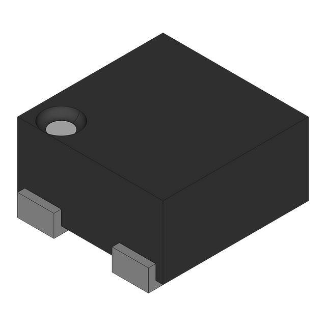
mDFN4 1.2 x 1.6 mm
NCV Prefix for Automotive and Other Applications Requiring
Unique Site and Control Change Requirements; AEC−Q100
Qualified and PPAP Capable
This is a Pb−Free Device
www.onsemi.com
MARKING
DIAGRAM
1
3A M
UDFN4
CASE 517CE
3A
M
= Specific Device Code
= Date Code
PINOUT DIAGRAM
IN
OUT
PAD1
GND
EN
(Top View)
Typical Applications
•
•
•
•
•
Mobile Phones
Tablets
Digital Cameras
GPS
Computers
Vbat
1 mF
ORDERING INFORMATION
See detailed ordering and shipping information on page 8 of
this data sheet.
IN
OUT
NCP330
EN
1 mF
GND
EN
USB
Port
VBUS
D+
D−
GND
4
IN
CMIC OUT
SBC Charger
SYSTEM
Supply
HS
Monitoring USB
Signal
Routing
Accessory
Detection and ID
I@C
Figure 1. Typical Application Circuit
© Semiconductor Components Industries, LLC, 2015
April, 2015 − Rev. 2
1
Publication Order Number:
NCP330/D
�NCP330
PIN FUNCTION DESCRIPTION
Pin Name
Pin
Number
Type
Description
IN
1
POWER
Power−switch input voltage; connect a 1 mF or greater ceramic capacitor from IN to GND as
close as possible to the IC.
GND
2
POWER
Ground connection;
EN
3
INPUT
OUT
4
OUTPUT
Power−switch output; connect a 1 mF ceramic capacitor from OUT to GND as close as possible to the IC is recommended.
POWER
Exposed pad can be connected to GND plane for dissipation purpose or any other thermal
plane.
PAD1
Enable input, logic high turns on power switch.
BLOCK DIAGRAM
IN: Pin1
OUT: Pin 4
1 mF
Gate driver and soft
start control
Battery
VREF
Charge
Pump
EN: 3
EN block
2
Figure 2. Block Diagram
www.onsemi.com
2
�NCP330
MAXIMUM RATINGS
Rating
Symbol
Value
Unit
VEN , VIN , VOUT
−0.3 to + 7.0
V
From IN to OUT Pins: Input/Output
VIN , VOUT
−7.0 to + 7.0
V
ESD Withstand Voltage (IEC 61000−4−2) (Note 1)
(IN and OUT when bypassed with 1.0 mF capacitor minimum)
ESD IEC
15 Air, 8 contact
kV
Human Body Model (HBM) ESD Rating are (Notes 2 and 3)
ESD HBM
4000
V
Machine Model (MM) ESD Rating are (Notes 2 and 3)
ESD MM
200
V
LU
100
TJ
−40 to + 125
°C
Storage Temperature Range
TSTG
−40 to + 150
°C
Moisture Sensitivity (Note 5)
MSL
Level 1
IN, OUT, EN, Pins:
Latch−up protection (Note 4)
− Pins IN, OUT, EN
mA
Maximum Junction Temperature Range
Stresses exceeding those listed in the Maximum Ratings table may damage the device. If any of these limits are exceeded, device functionality
should not be assumed, damage may occur and reliability may be affected.
1. Guaranteed by design.
2. According to JEDEC standard JESD22−A108.
3. This device series contains ESD protection and passes the following tests:
Human Body Model (HBM) ±2.0 kV per JEDEC standard: JESD22−A114 for all pins.
Machine Model (MM) ±200 V per JEDEC standard: JESD22−A115 for all pins.
4. Latch up Current Maximum Rating: ±100 mA per JEDEC standard: JESD78 class II.
5. Moisture Sensitivity Level (MSL): 1 per IPC/JEDEC standard: J−STD−020.
RECOMMENDED OPERATING CONDITIONS
Symbol
Parameter
VIN
Operational Power Supply
VEN
Enable Voltage
Conditions
Min
Typ
Max
Unit
1.8
5.5
V
0
5.5
TA
Ambient Temperature Range
− 40
25
+ 85
°C
TJ
Junction Temperature Range
− 40
25
+ 125
°C
CIN
Decoupling input capacitor
COUT
Decoupling output capacitor
RqJA
Thermal Resistance Junction to Air
IOUT
Maximum DC current
I peak
PD
Maximum Peak current
Power Dissipation Rating (Note 7)
USB port per Hub
UDFN−4 package (Note 6)
1
mF
1
mF
°C/W
170
UDFN−4 package
3
1 ms at 217 Hz (GSM calibration)
5
TA ≤ 25°C
UDFN−4 package
0.58
TA = 85°C
UDFN−4 package
0.225
A
A
W
Functional operation above the stresses listed in the Recommended Operating Ranges is not implied. Extended exposure to stresses beyond
the Recommended Operating Ranges limits may affect device reliability.
6. The RqJA is dependent of the PCB heat dissipation.
7. The maximum power dissipation (PD) is given by the following formula:
PD +
www.onsemi.com
3
T JMAX * T A
R qJA
�NCP330
ELECTRICAL CHARACTERISTICS Min & Max Limits apply for TA between −40°C to +85°C and TJ up to + 125 °C for VIN between
1.8 V to 5.5 V (Unless otherwise noted). Typical values are referenced to TA = + 25 °C and VIN = 5 V.
Symbol
Parameter
Conditions
Min
Typ
Max
Unit
POWER SWITCH
Static drain−source on−state
resistance
VIN = 3 V,
VIN = 5 V
TR
Output rise time
VIN = 5 V
CLOAD = 1 mF,
RLOAD = 125 W (Note 8)
TF
Output fall time
VIN = 5 V
CLOAD = 100 mF,
RLOAD = 40 W (Note 8)
Ton
Gate turn on
VIN = 5 V
From Vin applied to VOUT =
10% of fully on
VIN = 3 V
From Vin applied to VOUT =
10% of fully on (Note 9)
RDS(on)
TJ = 25°C
26
−40°C < TJ < 125°C
mW
50
0.5
2
4
4
0.5
2
ms
ms
4
ms
3
ENABLE INPUT EN
VIH
High−level input voltage
VIL
Low−level input voltage
Rpd
En pull−down resistor
Rpu
En pull−up resistor
1.15
V
0.85
V
1
MW
1.5
MW
REVERSE−LEAKAGE PROTECTION
IREV
Reverse−current protection
VIN = 0 V, Vout = 4.2 V (part disable), TJ = 25°C
0.15
1
mA
No load
100
200
mA
QUIESCENT CURRENT
Iq
Current consumption
Product parametric performance is indicated in the Electrical Characteristics for the listed test conditions, unless otherwise noted. Product
performance may not be indicated by the Electrical Characteristics if operated under different conditions.
8. Parameters are guaranteed for CLOAD and RLOAD connected to the OUT pin with respect to the ground.
9. Guaranteed by characterization.
www.onsemi.com
4
�NCP330
TYPICAL CHARACTERISTICS
0.35
TA = 85°C
120
IREV, REVERSE CURRENT (mA)
Iq, SUPPLY CURRENT (mA)
140
TA = 25°C
100
TA = −40°C
80
60
40
20
0
0.30
0.25
TA = 85°C
0.20
0.15
TA = −40°C
0.10
0.05
TA = 25°C
0
1.5
2.0
2.5
3.0
3.5
4.0
4.5
5.0
1.5
5.5
2.0
2.5
3.0
3.5
4.0
4.5
5.0
5.5
VIN, INPUT VOLTAGE (V)
VOUT, OUTPUT VOLTAGE (V)
Figure 3. Supply Current vs. Voltage
Figure 4. Reverse Current vs. Output Voltage
50
50
45
45
40
40
IOUT = 2 A
RDS(on) (mW)
RDS(on) (mW)
IOUT = 3 A
IOUT = 3 A
35
IOUT = 2 A
30
IOUT = 1 A
IOUT = 0.5 A
25
IOUT = 1 A
30
25
20
20
1.8
3.0
4.2
5.4
1.8
3.0
4.2
5.4
VIN, INPUT VOLTAGE (V)
VIN, INPUT VOLTAGE (V)
Figure 5. RDS(on) vs. VIN Voltage at 255C
Figure 6. RDS(on) vs. VIN Voltage at 855C
50
50
45
45
40
40
RDS(on) (mW)
RDS(on) (mW)
IOUT = 0.5 A
35
35
30
IOUT = 2 A
VIN = 1.8 V
35
VIN = 3.0 V
30
VIN = 5.5 V
IOUT = 3 A
25
VIN = 5.0 V
25
IOUT = 1 A
20
1.8
3.0
IOUT = 0.5 A
4.2
20
5.4
0
0.5
1.0
1.5
2.0
2.5
3.0
VIN, INPUT VOLTAGE (V)
IOUT, OUTPUT CURRENT (A)
Figure 7. RDS(on) vs. VIN Voltage at −405C
Figure 8. RDS(on) vs. IOUT at 255C
www.onsemi.com
5
3.5
�NCP330
TYPICAL CHARACTERISTICS
50
TJ, JUNCTION TEMPERATURE (°C)
90
RDS(on) (mW)
45
40
35
30
25
20
80
70
60
VIN = 3.0 V
50
VIN = 5.5 V
40
VIN = 5.0 V
30
20
10
0
0
0.5
1.0
2.0
1.5
2.5
3.0
3.5
0
0.5
1.0
1.5
2.0
2.5
IOUT, OUTPUT CURRENT (A)
IOUT, OUTPUT CURRENT (A)
Figure 9. RDS(on) vs. IOUT at 855C
Figure 10. Junction Temperature vs. IOUT
1.02
EN PIN THRESHOLD (V)
1.01
VIH vs. VIN
1.00
VIL vs. VIN
0.99
0.98
0.97
0.96
0.95
0.94
0
1
2
3
4
5
6
VIN, INPUT VOLTAGE (V)
Figure 11. Logic Threshold vs. VIN
Figure 12. TON Time on 75 mA Load
Figure 13. TOFF Time on 75 mA Load
Figure 14. TON Time on 800 mA Load
www.onsemi.com
6
3.0
�NCP330
TYPICAL CHARACTERISTICS
Figure 15. TOFF Time on 800 mA Load
Figure 16. TON Time on 2 A Load
Figure 17. TOFF Time on 2.3 A Load
www.onsemi.com
7
�NCP330
FUNCTIONAL DESCRIPTION
Overview
Blocking Control
The NCP330 is a high side N−channel MOSFET power
distribution switch designed to connect external voltage
directly to the system. The high side MOSFET is
automatically turned on if the Vin voltage is applied thanks
to internal pull up connected between Vin and EN pin. The
turned off is obtained by Vin removal. Due to the soft start
circuitry, NCP330 is able to limit large voltage surges.
The blocking control circuitry switches the bulk of the
power NMOS. When the part is off (No VIN or EN tied to
GND externally) , the body diode limits the leakage current
IREV from OUT to IN. In this mode, anode of the body diode
is connected to IN pin and cathode is connected to OUT pin.
In operating condition, anode of the body diode is connected
to OUT pin and cathode is connected to IN pin preventing
the discharge of the power supply.
Enable input
Enable pin is an active high. The part is off when Vin is not
present, limiting current consumption from battery to OUT
pin.
In the other side, the part is automatically turned on when
VIN is applied.
Cin Capacitor
A IN capacitor, 1 mF, at least, capacitor must be placed as
close as possible the part to be Compliant with
IEC61000−4−2 (Level 4).
Cout Capacitor
Depending on the sinking current during system start up
and system turn off, a capacitor must be placed on the output.
A 1 mF is strongly recommended but can be decreased down
to 100 nF if the above two sequences are well controlled and
parasitic inductance connected on the Vout line is negligible.
APPLICATION INFORMATION
Power Dissipation
PCB Recommendations
The device’s junction temperature depends on different
contributor factor such as board layout, ambient
temperature, device environment, etc... Yet, the main
contributor in term of junction temperature is the power
dissipation of the power MOSFET. Assuming this, the
power dissipation and the junction temperature in normal
mode can be calculated with the following equations:
The NCP330 integrates an up to 3 A rated NMOS FET,
and the PCB design rules must be respected to properly
evacuate the heat out of the silicon. The mDFN4 PAD1 must
be connected to ground plane to increase the heat transfer if
necessary. By increasing PCB area, the RqJA of the package
can be decreased, allowing higher power dissipation.
P D + R DS(on)
ǒIOUTǓ
2
PD
= Power dissipation (W)
RDS(on)
IOUT
= Power MOSFET on resistance (W)
= Output current (A)
TJ + PD
R qJA ) T A
TJ
= Junction temperature (°C
RqJA
TA
= Package thermal resistance (°C/W)
= Ambient temperature (°C)
ORDERING INFORMATION
Marking
Package
Shipping†
NCP330MUTBG
3A
3V
UDFN4
(Pb−Free)
3000 / Tape & Reel
NCV330MUTBG*
Device
†For information on tape and reel specifications, including part orientation and tape sizes, please refer to our Tape and Reel Packaging
Specifications Brochure, BRD8011/D.
*NCV Prefix for Automotive and Other Applications Requiring Unique Site and Control Change Requirements; AEC−Q100 Qualified and PPAP
Capable.
www.onsemi.com
8
�MECHANICAL CASE OUTLINE
PACKAGE DIMENSIONS
UDFN4 1.2x1.6, 0.5P
CASE 517CE
ISSUE B
1
SCALE 4:1
L
L
A
B
D
L1
ÉÉ
ÉÉ
PIN ONE
REFERENCE
2X
DETAIL A
ALTERNATE TERMINAL
CONSTRUCTIONS
E
0.05 C
2X
ÉÉ
ÉÉ
0.05 C
TOP VIEW
EXPOSED Cu
(A3)
DETAIL B
A
0.05 C
MOLD CMPD
DETAIL B
ALTERNATE
CONSTRUCTION
0.05 C
SIDE VIEW
A1 C
SEATING
PLANE
D2
DETAIL A
1
b
0.05
4X
2
M
NOTES:
1. DIMENSIONING AND TOLERANCING PER
ASME Y14.5M, 1994.
2. CONTROLLING DIMENSION: MILLIMETERS.
3. DIMENSION b APPLIES TO PLATED TERMINAL
AND IS MEASURED BETWEEN 0.15 AND
0.20 mm FROM THE TERMINAL TIPS.
4. PACKAGE DIMENSIONS EXCLUSIVE OF
BURRS AND MOLD FLASH.
DIM
A
A1
A3
b
D
D2
E
E2
e
L
L1
MILLIMETERS
MIN
NOM MAX
0.45
0.50
0.55
0.05
0.00
−−−
0.13 REF
0.35
0.25
0.30
1.20 BSC
0.96
0.76
0.86
1.60 BSC
0.60
0.40
0.50
0.50 BSC
0.40
0.20
0.30
−−−
−−−
0.15
GENERIC
MARKING DIAGRAM*
XX M
NOTE 3
E2
e
C A B
DATE 03 APR 2012
4
3
4X
e/2
L
BOTTOM VIEW
RECOMMENDED
MOUNTING FOOTPRINT*
0.86
XX = Specific Device Code
M = Date Code
*This information is generic. Please refer to
device data sheet for actual part marking.
Pb−Free indicator, “G” or microdot “ G”,
may or may not be present.
4X
0.25
PACKAGE
OUTLINE
1.90
0.50
1
0.50
PITCH
4X
0.45
DIMENSIONS: MILLIMETERS
*For additional information on our Pb−Free strategy and soldering
details, please download the ON Semiconductor Soldering and
Mounting Techniques Reference Manual, SOLDERRM/D.
DOCUMENT NUMBER:
DESCRIPTION:
98AON66552E
UDFN4, 1.2X1.6, 0.5P
Electronic versions are uncontrolled except when accessed directly from the Document Repository.
Printed versions are uncontrolled except when stamped “CONTROLLED COPY” in red.
PAGE 1 OF 1
ON Semiconductor and
are trademarks of Semiconductor Components Industries, LLC dba ON Semiconductor or its subsidiaries in the United States and/or other countries.
ON Semiconductor reserves the right to make changes without further notice to any products herein. ON Semiconductor makes no warranty, representation or guarantee regarding
the suitability of its products for any particular purpose, nor does ON Semiconductor assume any liability arising out of the application or use of any product or circuit, and specifically
disclaims any and all liability, including without limitation special, consequential or incidental damages. ON Semiconductor does not convey any license under its patent rights nor the
rights of others.
© Semiconductor Components Industries, LLC, 2019
www.onsemi.com
�onsemi,
, and other names, marks, and brands are registered and/or common law trademarks of Semiconductor Components Industries, LLC dba “onsemi” or its affiliates
and/or subsidiaries in the United States and/or other countries. onsemi owns the rights to a number of patents, trademarks, copyrights, trade secrets, and other intellectual property.
A listing of onsemi’s product/patent coverage may be accessed at www.onsemi.com/site/pdf/Patent−Marking.pdf. onsemi reserves the right to make changes at any time to any
products or information herein, without notice. The information herein is provided “as−is” and onsemi makes no warranty, representation or guarantee regarding the accuracy of the
information, product features, availability, functionality, or suitability of its products for any particular purpose, nor does onsemi assume any liability arising out of the application or use
of any product or circuit, and specifically disclaims any and all liability, including without limitation special, consequential or incidental damages. Buyer is responsible for its products
and applications using onsemi products, including compliance with all laws, regulations and safety requirements or standards, regardless of any support or applications information
provided by onsemi. “Typical” parameters which may be provided in onsemi data sheets and/or specifications can and do vary in different applications and actual performance may
vary over time. All operating parameters, including “Typicals” must be validated for each customer application by customer’s technical experts. onsemi does not convey any license
under any of its intellectual property rights nor the rights of others. onsemi products are not designed, intended, or authorized for use as a critical component in life support systems
or any FDA Class 3 medical devices or medical devices with a same or similar classification in a foreign jurisdiction or any devices intended for implantation in the human body. Should
Buyer purchase or use onsemi products for any such unintended or unauthorized application, Buyer shall indemnify and hold onsemi and its officers, employees, subsidiaries, affiliates,
and distributors harmless against all claims, costs, damages, and expenses, and reasonable attorney fees arising out of, directly or indirectly, any claim of personal injury or death
associated with such unintended or unauthorized use, even if such claim alleges that onsemi was negligent regarding the design or manufacture of the part. onsemi is an Equal
Opportunity/Affirmative Action Employer. This literature is subject to all applicable copyright laws and is not for resale in any manner.
PUBLICATION ORDERING INFORMATION
LITERATURE FULFILLMENT:
Email Requests to: orderlit@onsemi.com
onsemi Website: www.onsemi.com
◊
TECHNICAL SUPPORT
North American Technical Support:
Voice Mail: 1 800−282−9855 Toll Free USA/Canada
Phone: 011 421 33 790 2910
Europe, Middle East and Africa Technical Support:
Phone: 00421 33 790 2910
For additional information, please contact your local Sales Representative
�


 工商网监
湘ICP备2023018690号
工商网监
湘ICP备2023018690号
