NCP370GEVB
NCP370 Over Voltage
Protection Controller with
Reverse Charge Control
Evaluation Board User's
Manual
http://onsemi.com
EVAL BOARD USER’S MANUAL
Description
The NCP370 is an overvoltage, overcurrent and reverse control
device. Two main modes are available by setting logic pins.
First mode is Direct Mode from Wall Adapter to the system. In this
mode the system is both positive and negative overvoltage protected
up to +28 V and down to −28 V. The wall adapter is disconnected from
the system if the input voltage exceeds the overvoltage (OVLO) or
undervoltage (UVLO) thresholds. At powerup, the Vout turns on
30 ms after the Vin exceeds the undervoltage threshold.
The second mode, called the Reverse Mode, allows an external
accessory to be powered by the system battery or a boost converter.
Here, the external accessory would be connected to the device input
(bottom connector of system) and the device battery would be at the
device output. In this case, overcurrent protection is activated to
prevent accessory faults and battery discharge. Thanks to the NCP370
using an internal NMOS, the system cost and the PCB area of the
application board are minimized. The NCP370 provides a negative
going flag (FLAG(BAR)) output which alerts the system that a fault
has occurred. In addition, the device has ESD protected input (15 kV
Air) when bypassed with a 1.0 mF or larger capacitor.
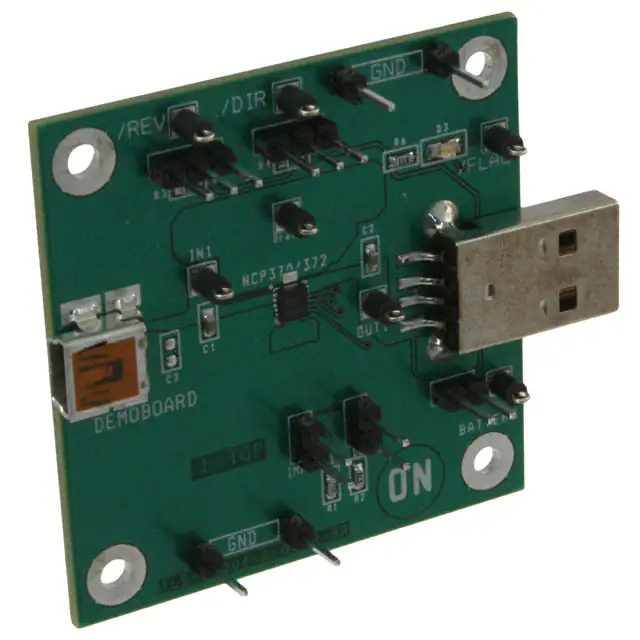
Figure 1. NCP370GEVB Board Picture
© Semiconductor Components Industries, LLC, 2011
August, 2011 − Rev. 3
1
Publication Order Number:
EVBUM2015/D
�NCP370GEVB
Figure 2. NCP370GEVB Board Schematic
http://onsemi.com
2
�NCP370GEVB
Table 1. BILL OF MATERIALS
Quantity
Designation
Manufacturer
1
NCP370 LLGA3x3
ON Semiconductor
2
C1 (Cin), C2 (Cout)
Murata –
GRM188R61E105KA12D
1
C3 (ID): not mounted
13
Test points:IN1, OUT1, BATTERY, FLAG, DRAIN, REV, DIR
1
J13 (USB IN)
1
Digi key
Specifications
Over voltage protection
490-3897-1-ND
1 mF 25V X5R CMS0805
5001K-ND
Hole diameter: 1.3mm
Molex
WM17116CT-ND
5 pins USB miniB
J12. (USB OUT)
Molex
WM17118-ND
4 pins USB A
1
FLAG
rohm
511-1287-ND
Green LED 0805
1
R6
susumu
Rr08p(value)dct-nd
1 kW. CMS0603 0.5%
2
R3, R4
susumu
Rr08p(value)dct-nd
100 kW. CMS0603 0.5%
Not
mounted
R5,R7,R8,R9 (USB data)
1
R1
susumu
Rr08p(value)bct-nd
69.8k W. CMS0603 0.5%
1
R2
susumu
Rr08p(value)bct-nd
16.9k W. CMS0603 0.5%
4
GND jumper: J7, J10
WM8083-ND
Jumper Ground 1mm pitch
10.16 mm
1x3
REV
WM8083-ND
SMB R 114 665
PCB Plated Gold
1x3
DIR
WM8083-ND
SMB R 114 665
PCB Plated Gold
1x2
Imax
WM8083-ND
SMB R 114 665
PCB Plated Gold
1x2
I2
WM8083-ND
SMB R 114 665
PCB Plated Gold
1x2
Battery
WM8083-ND
SMB R 114 665
PCB Plated Gold
http://onsemi.com
3
�NCP370GEVB
PCB
Figure 3. NCP370GEVB Board Layout (Top View)
Figure 4. NCP370GEVB Board Layout (Bottom View)
http://onsemi.com
4
�NCP370GEVB
CONNECTING PROCESS
1. Place /REV strap and /DIR strap on left side (“1” logic) (connected to Vbat, through pull up resistor)
2. Let Battery strap opened.
3. Connect a Battery or power supply (4.2 V) on Battery test point (min 2 A capability).
http://onsemi.com
5
�NCP370GEVB
4. Connect strap on lim.
ILIM PIN (7)
SW2 (2)
SW1 (IMAX)
R1 = 70k
R2 = 14k
http://onsemi.com
6
�NCP370GEVB
5. Select I limit threshold with pull down resistors connected on pin 7:
SW1
SW2
IOCP
0
0
500 mA
0
1
1A
1
0
1.5 A
1
1
1.5 A
R1 = 70K
R2 = 14K
Disable Mode:
6. Connect 10 V capability Vin Supply on IN1 test point.
a.) Set power supply to 5 V ⇒ Check Vout = 0 V and LED = off
http://onsemi.com
7
�NCP370GEVB
Direct Mode:
7. Switch /DIR from left to right, 1 logic level to 0 logic level
8. Check Vout = 5 V and Flag LED is still off
9. Set Vin = 7 V
10. Check Flag LED = on, and Vout is 0 V.
11. Switch /REV from left to right, 1 logic level to 0 logic level
12. Check Flag LED = off, and Vout = Vin = 7 V.
Disconnect Vin Supply.
http://onsemi.com
8
�NCP370GEVB
Reverse Mode:
13. Connect Set /DIR = 1, /REV = 1
Disconnect Vin Power Supply from IN test points.
Connect accessory on IN1 or IN2 test points.
Put strap to connect Battery to Vout
14. Set /DIR = 1, /REV = 0: Vout = Vin
If I accessory < I limit then Vin = Vout − Rdson x I
If I accessory > I limit then Vin = 0 (Current regulation)
Power off.
15. Set /DIR = 1, /REV = 1
16. Disconnect accessory
17. Disconnect Battery
http://onsemi.com
9
�onsemi,
, and other names, marks, and brands are registered and/or common law trademarks of Semiconductor Components Industries, LLC dba “onsemi” or its affiliates
and/or subsidiaries in the United States and/or other countries. onsemi owns the rights to a number of patents, trademarks, copyrights, trade secrets, and other intellectual property. A
listing of onsemi’s product/patent coverage may be accessed at www.onsemi.com/site/pdf/Patent−Marking.pdf. onsemi is an Equal Opportunity/Affirmative Action Employer. This
literature is subject to all applicable copyright laws and is not for resale in any manner.
The evaluation board/kit (research and development board/kit) (hereinafter the “board”) is not a finished product and is not available for sale to consumers. The board is only intended
for research, development, demonstration and evaluation purposes and will only be used in laboratory/development areas by persons with an engineering/technical training and familiar
with the risks associated with handling electrical/mechanical components, systems and subsystems. This person assumes full responsibility/liability for proper and safe handling. Any
other use, resale or redistribution for any other purpose is strictly prohibited.
THE BOARD IS PROVIDED BY ONSEMI TO YOU “AS IS” AND WITHOUT ANY REPRESENTATIONS OR WARRANTIES WHATSOEVER. WITHOUT LIMITING THE FOREGOING,
ONSEMI (AND ITS LICENSORS/SUPPLIERS) HEREBY DISCLAIMS ANY AND ALL REPRESENTATIONS AND WARRANTIES IN RELATION TO THE BOARD, ANY
MODIFICATIONS, OR THIS AGREEMENT, WHETHER EXPRESS, IMPLIED, STATUTORY OR OTHERWISE, INCLUDING WITHOUT LIMITATION ANY AND ALL
REPRESENTATIONS AND WARRANTIES OF MERCHANTABILITY, FITNESS FOR A PARTICULAR PURPOSE, TITLE, NON−INFRINGEMENT, AND THOSE ARISING FROM A
COURSE OF DEALING, TRADE USAGE, TRADE CUSTOM OR TRADE PRACTICE.
onsemi reserves the right to make changes without further notice to any board.
You are responsible for determining whether the board will be suitable for your intended use or application or will achieve your intended results. Prior to using or distributing any systems
that have been evaluated, designed or tested using the board, you agree to test and validate your design to confirm the functionality for your application. Any technical, applications or
design information or advice, quality characterization, reliability data or other services provided by onsemi shall not constitute any representation or warranty by onsemi, and no additional
obligations or liabilities shall arise from onsemi having provided such information or services.
onsemi products including the boards are not designed, intended, or authorized for use in life support systems, or any FDA Class 3 medical devices or medical devices with a similar
or equivalent classification in a foreign jurisdiction, or any devices intended for implantation in the human body. You agree to indemnify, defend and hold harmless onsemi, its directors,
officers, employees, representatives, agents, subsidiaries, affiliates, distributors, and assigns, against any and all liabilities, losses, costs, damages, judgments, and expenses, arising
out of any claim, demand, investigation, lawsuit, regulatory action or cause of action arising out of or associated with any unauthorized use, even if such claim alleges that onsemi was
negligent regarding the design or manufacture of any products and/or the board.
This evaluation board/kit does not fall within the scope of the European Union directives regarding electromagnetic compatibility, restricted substances (RoHS), recycling (WEEE), FCC,
CE or UL, and may not meet the technical requirements of these or other related directives.
FCC WARNING – This evaluation board/kit is intended for use for engineering development, demonstration, or evaluation purposes only and is not considered by onsemi to be a finished
end product fit for general consumer use. It may generate, use, or radiate radio frequency energy and has not been tested for compliance with the limits of computing devices pursuant
to part 15 of FCC rules, which are designed to provide reasonable protection against radio frequency interference. Operation of this equipment may cause interference with radio
communications, in which case the user shall be responsible, at its expense, to take whatever measures may be required to correct this interference.
onsemi does not convey any license under its patent rights nor the rights of others.
LIMITATIONS OF LIABILITY: onsemi shall not be liable for any special, consequential, incidental, indirect or punitive damages, including, but not limited to the costs of requalification,
delay, loss of profits or goodwill, arising out of or in connection with the board, even if onsemi is advised of the possibility of such damages. In no event shall onsemi’s aggregate liability
from any obligation arising out of or in connection with the board, under any theory of liability, exceed the purchase price paid for the board, if any.
The board is provided to you subject to the license and other terms per onsemi’s standard terms and conditions of sale. For more information and documentation, please visit
www.onsemi.com.
PUBLICATION ORDERING INFORMATION
LITERATURE FULFILLMENT:
Email Requests to: orderlit@onsemi.com
onsemi Website: www.onsemi.com
◊
TECHNICAL SUPPORT
North American Technical Support:
Voice Mail: 1 800−282−9855 Toll Free USA/Canada
Phone: 011 421 33 790 2910
www.onsemi.com
1
Europe, Middle East and Africa Technical Support:
Phone: 00421 33 790 2910
For additional information, please contact your local Sales Representative
�