ON Semiconductor
Is Now
To learn more about onsemi™, please visit our website at
www.onsemi.com
onsemi and and other names, marks, and brands are registered and/or common law trademarks of Semiconductor Components Industries, LLC dba “onsemi” or its affiliates and/or
subsidiaries in the United States and/or other countries. onsemi owns the rights to a number of patents, trademarks, copyrights, trade secrets, and other intellectual property. A listing of onsemi
product/patent coverage may be accessed at www.onsemi.com/site/pdf/Patent-Marking.pdf. onsemi reserves the right to make changes at any time to any products or information herein, without
notice. The information herein is provided “as-is” and onsemi makes no warranty, representation or guarantee regarding the accuracy of the information, product features, availability, functionality,
or suitability of its products for any particular purpose, nor does onsemi assume any liability arising out of the application or use of any product or circuit, and specifically disclaims any and all
liability, including without limitation special, consequential or incidental damages. Buyer is responsible for its products and applications using onsemi products, including compliance with all laws,
regulations and safety requirements or standards, regardless of any support or applications information provided by onsemi. “Typical” parameters which may be provided in onsemi data sheets and/
or specifications can and do vary in different applications and actual performance may vary over time. All operating parameters, including “Typicals” must be validated for each customer application
by customer’s technical experts. onsemi does not convey any license under any of its intellectual property rights nor the rights of others. onsemi products are not designed, intended, or authorized
for use as a critical component in life support systems or any FDA Class 3 medical devices or medical devices with a same or similar classification in a foreign jurisdiction or any devices intended for
implantation in the human body. Should Buyer purchase or use onsemi products for any such unintended or unauthorized application, Buyer shall indemnify and hold onsemi and its officers, employees,
subsidiaries, affiliates, and distributors harmless against all claims, costs, damages, and expenses, and reasonable attorney fees arising out of, directly or indirectly, any claim of personal injury or death
associated with such unintended or unauthorized use, even if such claim alleges that onsemi was negligent regarding the design or manufacture of the part. onsemi is an Equal Opportunity/Affirmative
Action Employer. This literature is subject to all applicable copyright laws and is not for resale in any manner. Other names and brands may be claimed as the property of others.
�NCP4561
Ultra Low−Noise Low
Dropout Voltage Regulator
with 1.0 V ON/OFF Control
The NCP4561 is a Low DropOut (LDO) regulator featuring
excellent noise performances. Thanks to its innovative concept, the
circuit reaches an incredible 40 mVRMS noise level without an
external bypass capacitor. Housed in a small SOT−23 5 leads−like
package, it represents the ideal designer’s choice when space and
noise are at premium.
The absence of external bandgap capacitor unleashes the response
time to a wake−up signal and makes it stay within 40 ms (in repetitive
mode), pushing the NCP4561 as a natural candidate in portable
applications.
The NCP4561 also hosts a novel architecture which prevents
excessive undershoots when the regulator is the seat of fast transient
bursts, as in any bursting systems.
Finally, with a static line regulation better than −75 dB, it naturally
shields the downstream electronics against choppy lines.
Features
• Ultra Low−Noise: 150 nV/√Hz @ 100 Hz, 40 mVRMS 100 Hz −
•
•
•
•
•
•
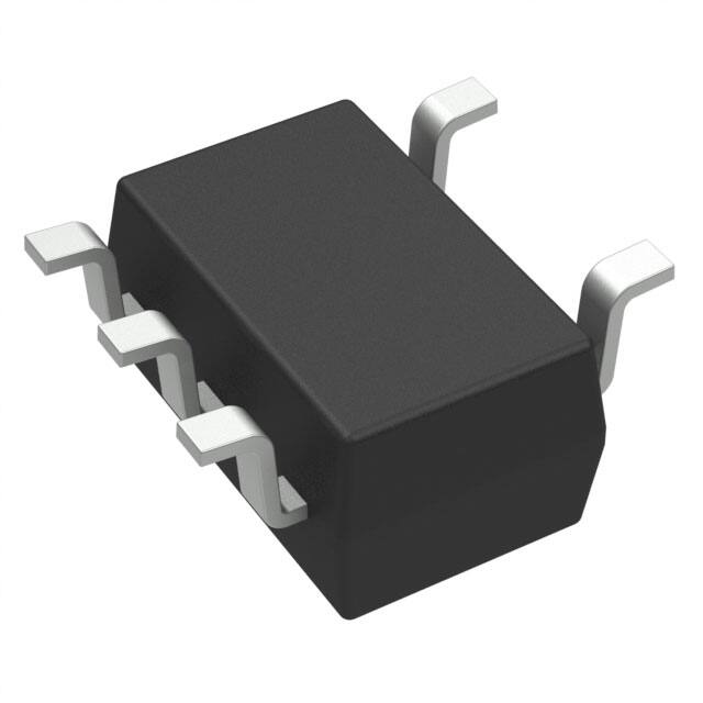
5
1
TSOP−5
SN SUFFIX
CASE 483
PIN CONNECTIONS AND
MARKING DIAGRAM
ON/OFF
1
GND
2
NC
3
5
Vin
4
Vout
P28YW
•
100 kHz Typical, Iout = 60 mA, Co = 1.0 mF
Fast Response Time from OFF to ON: 40 ms Typical at a 200 Hz
Repetition Rate
Ready for 1.0 V Platforms: ON with a 900 mV High Level
Nominal Output Current of 80 mA with a 100 mA Peak Capability
Typical Dropout of 90 mV @ 30 mA, 160 mV @ 80 mA
Ripple Rejection: 70 dB @ 1.0 kHz
1.5% Output Precision @ 25°C
Thermal Shutdown
http://onsemi.com
(Top View)
P28 = Device Code
Y
= Year
W = Work Week
Applications
• Noise Sensitive Circuits: VCOs RF Stages, etc.
• Bursting Systems (TDMA Phones)
• All Battery Operated Devices
ON/
OFF
1
NC
3
GND
2
On/Off
Band Gap
Reference
Thermal
Shutdown
*Current Limit
*Antisaturation Protection
*Load Transient Improvement
ORDERING INFORMATION
5
Vin
4
Vout
Device
Voltage
Output*
Shipping
NCP4561SN28T1
2.8 V
3000/Tape & Reel
* Contact your ON Semiconductor sales
representative for other output voltage values.
Figure 1. Simplified Block Diagram
© Semiconductor Components Industries, LLC, 2006
September, 2006 − Rev. 3
1
Publication Order Number:
NCP4561/D
�NCP4561
PIN FUNCTION DESCRIPTIONS
Pin #
Pin Name
Function
1
ON/OFF
Shuts or
wakes−up the IC
Description
2
GND
The IC’s ground
3
NC
None
It makes no arm to connect the pin to a known potential, like in a pin−to−pin
replacement case.
4
Vout
Delivers the
output voltage
This pin requires a 1.0 mF output capacitor to be stable.
5
Vin
Powers the IC
A positive voltage up to 12 V can be applied upon this pin.
A 900 mV level on this pin is sufficient to start the IC. A 150 mV shuts it down.
MAXIMUM RATINGS
Value
Rating
Pin #
Symbol
Min
Max
Unit
5
Vin
−
12
V
Power Supply Voltage
ESD Capability, HBM Model
All Pins
−
1.0
kV
ESD Capability, Machine Model
All Pins
−
200
V
W
Maximum Power Dissipation
NW Suffix, Plastic Package
Thermal Resistance Junction−to−Air
PD
−
RqJ−A
−
Internally
Limited
210
Operating Ambient Temperature
Maximum Junction Temperature (Note 1)
Maximum Operating Junction Temperature (Note 2)
TA
TJmax
TJ
−
−
−
−40 to +85
150
125
°C
Tstg
−
−60 to +150
°C
Storage Temperature Range
°C/W
ELECTRICAL CHARACTERISTICS
(For Typical Values TA = 25°C, for Min/Max values TA = −40°C to +85°C, Max TJ = 125°C unless otherwise noted)
Pin #
Symbol
Min
Typ
Max
Unit
Input Voltage Range
1
VON/OFF
0
−
Vin
V
ON/OFF Input Resistance
1
RON/OFF
−
250
−
kW
ON/OFF Control Voltages (Note 3)
Logic Zero, OFF State, IO = 50 mA
Logic One, ON State, IO = 50 mA
1
VON/OFF
−
900
−
−
150
−
Characteristics
Logic Control Specifications
mV
Currents Parameters
Current Consumption in OFF State
OFF Mode Current: Vin = Vout + 1.0 V, IO = 0, VOFF = 150 mV
IQOFF
−
0.1
2.0
mA
Current Consumption in ON State
ON Mode Current: Vin = Vout + 1.0 V, IO = 0, VON = 3.5 V
IQON
−
180
−
mA
Current Consumption in ON State, ON Mode
Saturation Current: Vin = Vout − 0.5 V, No Output Load
IQSAT
−
800
−
mA
Current Limit Vin = Voutnom + 1.0 V,
Output is brought to Voutnom − 0.3 V
IMAX
100
180
−
mA
1. Internally Limited by Shutdown.
2. Specifications are guaranteed below this value.
3. Voltage Slope should be Greater than 2.0 mV/ms.
http://onsemi.com
2
�NCP4561
ELECTRICAL CHARACTERISTICS (continued)
(For Typical Values TA = 25°C, for Min/Max values TA = −40°C to +85°C, Max TJ = 125°C unless otherwise noted)
Pin #
Symbol
Min
Typ
Max
Unit
Vout + 1.0 V < Vin < 6.0 V, TA = 25°C, 1.0 mA < Iout < 80 mA
4
Vout
2.758
2.8
2.842
V
Vout + 1.0 V < Vin < 6.0 V, TA = −40°C to +85°C, 1.0 mA < Iout < 80 mA
4
Vout
2.716
2.8
2.884
V
4/5
Regline
−
−
20
mV
4
Regload
−
−
40
mV
4
4
4
Vin−Vout
Vin−Vout
Vin−Vout
−
−
−
90
140
160
150
200
250
4/5
Ripple
−
−70
−
dB
−
150
−
nV/
√Hz
Characteristics
Output Voltages
Line and Load Regulation, Dropout Voltages
Line Regulation
Vout + 1.0 V < Vin < 12 V, Iout = 80 mA
Load Regulation
Vin = Vout + 1.0 V, Cout = 1.0 mF, Iout = 1.0 to 80 mA
Dropout Voltage (Note 4)
Iout = 30 mA
Iout = 60 mA
Iout = 80 mA
mV
Dynamic Parameters
Ripple Rejection
Vin = Vout + 1.0 V + 1.0 kHz 100 mVpp Sinusoidal Signal
Output Noise Density @ 1.0 kHz
4
RMS Output Noise Voltage
Cout = 1.0 mF, Iout = 50 mA, F = 100 Hz to 1.0 MHz
4
Noise
−
35
−
mV
Output Rise Time
Cout = 1.0 mF, Iout = 50 mA, 10% of Rising ON Signal to 90% of
Nominal Vout
4
trise
−
40
−
ms
−
−
125
°C
Thermal Shutdown
Thermal Shutdown
4. Vout is brought to Vout − 100 mV.
http://onsemi.com
3
�NCP4561
DEFINITIONS
Load Regulation
Line Regulation
The change in output voltage for a change in output
current at a constant chip temperature.
The change in output voltage for a change in input voltage.
The measurement is made under conditions of low
dissipation or by using pulse technique such that the average
chip temperature is not significantly affected. One usually
distinguishes static line regulation or DC line regulation (a
DC step in the input voltage generates a corresponding step
in the output voltage) from ripple rejection or audio
susceptibility where the input is combined with a frequency
generator to sweep from a few hertz up to a defined
boundary while the output amplitude is monitored.
Dropout Voltage
The input/output differential at which the regulator output
no longer maintains regulation against further reductions in
input voltage. Measured when the output drops 100 mV
below its nominal value (which is measured at 1.0 V
differential value). The dropout level is affected by the chip
temperature, load current and minimum input supply
requirements.
Thermal Protection
Output Noise Voltage
This is the integrated value of the output noise over a
specified frequency range. Input voltage and output current
are kept constant during the measurement. Results are
expressed in mVRMS.
Internal thermal shutdown circuitry is provided to protect
the integrated circuit in the event that the maximum junction
temperature is exceeded. When activated at typically 125°C,
the regulator turns off. This feature is provided to prevent
catastrophic failures from accidental overheating.
Maximum Power Dissipation
Maximum Package Power Dissipation
The maximum total dissipation for which the regulator
will operate within its specs.
The maximum power package power dissipation is the
power dissipation level at which the junction temperature
reaches its maximum operating value, i.e. 125°C.
Depending on the ambient temperature, it is possible to
calculate the maximum power dissipation and thus the
maximum available output current.
Quiescent Current
The quiescent current is the current which flows through
the ground when the LDO operates without a load on its
output: internal IC operation, bias, etc. When the LDO
becomes loaded, this term is called the Ground current. It is
actually the difference between the input current (measured
through the LDO input pin) and the output current.
http://onsemi.com
4
�NCP4561
TYPICAL CHARACTERISTICS
6.000
210
5.000
4.500
4.000
−40°C
QUIESCENT CURRENT (mA)
GROUND CURRENT (mA)
5.500
25°C
3.500
3.000
2.500
85°C
2.000
1.500
1.000
0.500
0.000
0
20
40
80
60
100
200
195
190
185
−60
−40
−20
0
20
40
60
80
100
OUTPUT CURRENT (mA)
AMBIENT TEMPERATURE (°C)
Figure 2. Ground Current vs. Output Current
Figure 3. Quiescent Current vs. Temperature
2.810
200
2.805
150
OUTPUT VOLTAGE (V)
85°C
DROPOUT (mV)
205
25°C
100
−40°C
50
85°C
2.800
2.795
25°C
2.790
2.785
2.780
−40°C
2.775
2.770
2.765
2.760
00
−20
40
60
80
2.755
100
0
20
40
60
80
OUTPUT CURRENT (mA)
OUTPUT CURRENT (mA)
Figure 4. Dropout vs. Output Current
Figure 5. Output Voltage vs. Output Current
100
OUTPUT NOISE SPECTRAL DENSITY
180
1000
140
NOISE (nV/sqrt Hz)
DROPOUT VOLTAGE (mV)
Vin = Vout + 1
Cout = 1 mF
IO = 10 & 50 mA
80 mA
160
120
60 mA
100
80
30 mA
60
40
100
10
RMS Noise
10 Hz to 100 kHz: 36 mV
10 Hz to 1 MHz: 47 mV
20
0
−60
−40
−20
0
20
40
60
80
1
0.01
100
0.1
1
10
100
1000
FREQUENCY (kHz)
TEMPERATURE (°C)
Figure 6. Dropout Voltage vs. Temperature
Figure 7. Typical Noise Density Performance
http://onsemi.com
5
�NCP4561
POWER SUPPLY REJECTION RATIO
Mag (dB)
Vin = Vout + 1
Cout = 1 mF
Iload = 10 mA
−7.50
−15.00
PSSR (dB)
−22.50
−30.00
−37.50
−45.00
−52.50
−60.00
−67.50
10
100
1k
10 k
100 k
1M
FREQUENCY (Hz)
Figure 8. Typical Ripple Rejection Performance
(Iload = 10 mA)
POWER SUPPLY REJECTION RATIO
Mag (dB)
Vin = Vout + 1
Cout = 1 mF
Iload = 60 mA
−7.50
−15.00
PSSR (dB)
−22.50
−30.00
−37.50
−45.00
−52.50
−60.00
−67.50
10
100
1k
10 k
100 k
1M
FREQUENCY (Hz)
Figure 9. Typical Ripple Rejection Performance
(Iload = 60 mA)
http://onsemi.com
6
�NCP4561
APPLICATION HINTS
Input Decoupling
Protections
As with any regulator, it is necessary to reduce the
dynamic impedance of the supply rail that feeds the
component. A 1.0 mF capacitor either ceramic or tantalum is
recommended and should be connected close to the
NCP4561 package. Higher values will correspondingly
improve the overall line transient response.
The NCP4561 hosts several protections, giving natural
ruggedness and reliability to the products implementing the
component. The output current is internally limited to a
maximum value of 180 mA typical while temperature
shutdown occurs if the die heats up beyond 125°C. These
values let you assess the maximum differential voltage the
device can sustain at a given output current before its
protections come into play.
The maximum dissipation the package can handle is given
by:
Output Decoupling
Thanks to a novel concept, the NCP4561 is a stable
component and does not require any specific Equivalent
Series Resistance (ESR) neither a minimum output current.
Capacitors exhibiting ESRs ranging from a few mW up to
3.0 W can thus safely be used. The minimum decoupling
value is 1.0 mF and can be augmented to fulfill stringent load
transient requirements. The regulator accepts ceramic chip
capacitors as well as tantalum devices.
T
*T
A
P max + Jmax
R
qJA
If TJmax is limited to 125°C, then the NCP4561 can
dissipate up to 470 mW @ 25°C. The power dissipated by
the NCP4561 can be calculated from the following formula:
ǒ
Noise Decoupling
Ptot + V
Unlike other LDOs, the NCP4561 is a true low−noise
regulator. Without the need of an external bypass capacitor,
it typically reaches the incredible level of 40 mVRMS overall
noise between 100 Hz and 100 kHz. To give maximum
insight on noise specifications, ON Semiconductor includes
spectral density graphics. The classical bypass capacitor
impacts the start−up phase of standard LDOs. However,
thanks to its low−noise architecture, the NCP4561 operates
without a bypass element and thus offers a typical 40 ms
start−up phase.
in
I
Ǔ
(I ) ) ǒV * V outǓ
gnd out
in
I out
or
Vin max +
Ptot ) V out
I
gnd
I out
) I out
If a 80 mA output current is needed, the ground current is
extracted from the data−sheet curves: 4.0 mA @ 80 mA. For
a NCP4561SN28T1 (2.8 V) delivering 80 mA and operating
at 25°C, the maximum input voltage will then be 8.3 V.
http://onsemi.com
7
�NCP4561
Typical Applications
The following figure portrays the typical application of the NCP4561.
Dropout
Charge
SW*
4
Output
5
Input
C3
1.0 mF
3
2
+
1
NCP4561
+
R1
100 k
On/Off
C2
1.0 mF
*Enables the IC When Closed
Figure 10. A Typical Application Schematic
PCB Layout Considerations
inductances/capacitances are minimized. This layout is the
basis for the NCP4561 performance evaluation board. The
BNC connectors give the user an easy and quick evaluation
mean.
As for any low noise designs, particular care has to be
taken when tackling Printed Circuit Board (PCB) layout.
The figure below gives an example of a layout where stray
ON SEMICONDUCTOR
NCP4561 EVALUATION BOARD
DROPOUT
+
IN
_
+
OUT
_
ON Semiconductor
NCP4561 EVALUATION BOARD
OUT
OFF
ON
IN
ON/OFF
Figure 11. PCB Layout
http://onsemi.com
8
�NCP4561
Understanding the Load Transient Improvement
During this decreasing phase, the LDO stops the PNP bias
and one can consider the LDO asleep. If by misfortune a
current shot appears, the reaction time is incredibly
lengthened and a strong undershoot takes place. This
reaction is clearly not acceptable for line sensitive devices,
such as VCOs or other Radio−Frequency parts. This
problem is dramatically exacerbated when the output
current drops to zero rather than a few mA. In this later case,
the internal feedback network is the only discharge path,
accordingly lengthening the output voltage decay period.
The NCP4561 cures this problem by implementing a
clever design where the LDO detects the presence of the
overshoot and forces the system to go back to steady−state
as soon as possible, ready for the next shot, which positively
improves the response time and decreases the negative peak
voltage.
The NCP4561 features a novel architecture which allows
the user to easily implement the regulator in burst systems
where the time between two current shots is kept very small.
The quality of the transient response time is related to
many parameters, among which the closed−loop bandwidth
with the corresponding phase margin plays an important
role. However, other characteristics also come into play like
the series pass transistor saturation. When a current
perturbation suddenly appears on the output, e.g. a load
increase, the error amplifier reacts and actively biases the
PNP transistor. During this reaction time, the LDO is in
open−loop and the output impedance is rather high. As a
result, the voltage brutally drops until the error amplifier
effectively closes the loop and corrects the output error.
When the load disappears, the opposite phenomenon takes
place with a positive overshoot. The problem appears when
this overshoot decays down to the LDO steady−state value.
NCP4561 has a fast start−up phase
unacceptable level. NCP4561 offers the best of both worlds
since it no longer includes a bypass capacitor and starts in
less than 40 ms typically (Repetitive at 200 Hz). It also
ensures a low−noise level of 40 mVRMS 100 Hz−100 kHz.
The following picture details the typical NCP4561 startup
phase.
Thanks to the lack of bypass capacitor the NCP4561 is
able to supply its downstream circuitry as soon as the OFF
to ON signal appears. In a standard LDO, the charging time
of the external bypass capacitor hampers the response time.
A simple solution consists in suppressing this bypass
element but, unfortunately, the noise rises to an
Tek Run: 5.00 MS/s
Sample
Vout
500 mV/div
C4 High
2.78 V
C4 Mean
2.426 V
ON/OFF Pin Voltage
1 V/div
Ch3 1.00 V
Ch4 500 mV
M 10.0 ms Ch3
1.82 V
(Conditions: Vin = 3.8 V, Iload = 10 mA, Cout = 1 mF)
Figure 12. Start−Up Waveform
http://onsemi.com
9
�NCP4561
TYPICAL TRANSIENT RESPONSES
Tek Run: 1.00 MS/s
Sample
Vout
200 mV/div
C4 Max
2.800 V
C4 Mean
2.7840 V
C4 Min
2.720 V
Iload
20 mA/div
Ch2 20.0 mVW M 50.0 ms Ch2
Ch4 200 mV
38.4 mV
(Conditions: Vin = 3.8 V, Cout = 1 mF)
Figure 13. Load Current is Pulsed from 0 to 40 mA
Sample
Tek Run: 1.00 MS/s
Vout 200 mV/div
C4 Max
2.844 V
C4 Mean
2.7852 V
C4 Min
2.708 V
Iload
20 mA/div
Ch1 20.0 mVW
Ch4 200 mV
M 50.0 ms Ch1
78.8 mV
(Conditions: Vin = 3.8 V, Cout = 1 mF)
Figure 14. Load Current is Pulsed from 0 to 80 mA
http://onsemi.com
10
�NCP4561
TYPICAL TRANSIENT RESPONSES
Tek Run: 1.00 MS/s
Sample
Vout
200 mV/div
C4 Max
2.824 V
C4 Mean
2.7848 V
C4 Mean
2.776 V
Iload
20 mA/div
Ch2 20.0 mVW M 50.0 ms Ch2
Ch4 200 mV
38.4 mV
(Conditions: Vin = 3.8 V, Cout = 1 mF)
Figure 15. Load Current is Switched from 40 to 0 mA
Tek Stop: 1.00 MS/s
1930 Acgs
Vout 200 mV/div
C4 Max
2.844 V
C4 Mean
2.7848 V
C4 Min
2.708 V
Iload
20 mA/div
Ch1 20.0 mVW
Ch4 200 mV
M 50.0 ms Ch1
0V
(Conditions: Vin = 3.8 V, Cout = 1 mF)
Figure 16. Load Current is Switched from 80 to 0 mA
http://onsemi.com
11
�NCP4561
MINIMUM RECOMMENDED FOOTPRINT FOR SURFACE MOUNTED APPLICATIONS
Surface mount board layout is a critical portion of the
total design. The footprint for the semiconductor packages
must be the correct size to insure proper solder connection
interface between the board and the package. With the
correct pad geometry, the packages will self align when
subjected to a solder reflow process.
0.094
2.4
0.037
0.95
0.074
1.9
0.037
0.95
0.028
0.7
0.039
1.0
inches
mm
TSOP−5
(TSOP−5 is footprint compatible with SOT23−5)
ORDERING INFORMATION
Device
NCP4561SN28T1
Voltage Output*
Package
Shipping
2.8 V
TSOP−5
3000 Units /Tape & Reel
*Contact your ON Semiconductor sales representative for other output voltage values.
http://onsemi.com
12
�NCP4561
PACKAGE DIMENSIONS
TSOP−5
SN SUFFIX
PLASTIC PACKAGE
CASE 483−01
ISSUE B
NOTES:
1. DIMENSIONING AND TOLERANCING PER ANSI
Y14.5M, 1982.
2. CONTROLLING DIMENSION: MILLIMETER.
3. MAXIMUM LEAD THICKNESS INCLUDES LEAD
FINISH THICKNESS. MINIMUM LEAD THICKNESS
IS THE MINIMUM THICKNESS OF BASE
MATERIAL.
D
S
5
4
1
2
L
A
3
B
G
J
C
0.05 (0.002)
H
M
K
DIM
A
B
C
D
G
H
J
K
L
M
S
MILLIMETERS
MIN
MAX
2.90
3.10
1.30
1.70
0.90
1.10
0.25
0.50
0.85
1.05
0.013
0.100
0.10
0.26
0.20
0.60
1.25
1.55
0_
10 _
2.50
3.00
INCHES
MIN
MAX
0.1142 0.1220
0.0512 0.0669
0.0354 0.0433
0.0098 0.0197
0.0335 0.0413
0.0005 0.0040
0.0040 0.0102
0.0079 0.0236
0.0493 0.0610
0_
10 _
0.0985 0.1181
ON Semiconductor and
are registered trademarks of Semiconductor Components Industries, LLC (SCILLC). SCILLC reserves the right to make changes without further notice
to any products herein. SCILLC makes no warranty, representation or guarantee regarding the suitability of its products for any particular purpose, nor does SCILLC assume any liability
arising out of the application or use of any product or circuit, and specifically disclaims any and all liability, including without limitation special, consequential or incidental damages.
“Typical” parameters which may be provided in SCILLC data sheets and/or specifications can and do vary in different applications and actual performance may vary over time. All
operating parameters, including “Typicals” must be validated for each customer application by customer’s technical experts. SCILLC does not convey any license under its patent rights
nor the rights of others. SCILLC products are not designed, intended, or authorized for use as components in systems intended for surgical implant into the body, or other applications
intended to support or sustain life, or for any other application in which the failure of the SCILLC product could create a situation where personal injury or death may occur. Should
Buyer purchase or use SCILLC products for any such unintended or unauthorized application, Buyer shall indemnify and hold SCILLC and its officers, employees, subsidiaries, affiliates,
and distributors harmless against all claims, costs, damages, and expenses, and reasonable attorney fees arising out of, directly or indirectly, any claim of personal injury or death
associated with such unintended or unauthorized use, even if such claim alleges that SCILLC was negligent regarding the design or manufacture of the part. SCILLC is an Equal
Opportunity/Affirmative Action Employer. This literature is subject to all applicable copyright laws and is not for resale in any manner.
PUBLICATION ORDERING INFORMATION
LITERATURE FULFILLMENT:
Literature Distribution Center for ON Semiconductor
P.O. Box 5163, Denver, Colorado 80217 USA
Phone: 303−675−2175 or 800−344−3860 Toll Free USA/Canada
Fax: 303−675−2176 or 800−344−3867 Toll Free USA/Canada
Email: orderlit@onsemi.com
N. American Technical Support: 800−282−9855 Toll Free
USA/Canada
Europe, Middle East and Africa Technical Support:
Phone: 421 33 790 2910
Japan Customer Focus Center
Phone: 81−3−5773−3850
http://onsemi.com
13
ON Semiconductor Website: www.onsemi.com
Order Literature: http://www.onsemi.com/orderlit
For additional information, please contact your local
Sales Representative
NCP4561/D
�