ON Semiconductor
Is Now
To learn more about onsemi™, please visit our website at
www.onsemi.com
onsemi and and other names, marks, and brands are registered and/or common law trademarks of Semiconductor Components Industries, LLC dba “onsemi” or its affiliates and/or
subsidiaries in the United States and/or other countries. onsemi owns the rights to a number of patents, trademarks, copyrights, trade secrets, and other intellectual property. A listing of onsemi
product/patent coverage may be accessed at www.onsemi.com/site/pdf/Patent-Marking.pdf. onsemi reserves the right to make changes at any time to any products or information herein, without
notice. The information herein is provided “as-is” and onsemi makes no warranty, representation or guarantee regarding the accuracy of the information, product features, availability, functionality,
or suitability of its products for any particular purpose, nor does onsemi assume any liability arising out of the application or use of any product or circuit, and specifically disclaims any and all
liability, including without limitation special, consequential or incidental damages. Buyer is responsible for its products and applications using onsemi products, including compliance with all laws,
regulations and safety requirements or standards, regardless of any support or applications information provided by onsemi. “Typical” parameters which may be provided in onsemi data sheets and/
or specifications can and do vary in different applications and actual performance may vary over time. All operating parameters, including “Typicals” must be validated for each customer application
by customer’s technical experts. onsemi does not convey any license under any of its intellectual property rights nor the rights of others. onsemi products are not designed, intended, or authorized
for use as a critical component in life support systems or any FDA Class 3 medical devices or medical devices with a same or similar classification in a foreign jurisdiction or any devices intended for
implantation in the human body. Should Buyer purchase or use onsemi products for any such unintended or unauthorized application, Buyer shall indemnify and hold onsemi and its officers, employees,
subsidiaries, affiliates, and distributors harmless against all claims, costs, damages, and expenses, and reasonable attorney fees arising out of, directly or indirectly, any claim of personal injury or death
associated with such unintended or unauthorized use, even if such claim alleges that onsemi was negligent regarding the design or manufacture of the part. onsemi is an Equal Opportunity/Affirmative
Action Employer. This literature is subject to all applicable copyright laws and is not for resale in any manner. Other names and brands may be claimed as the property of others.
�NCP4623
150 mA, Wide Input Voltage
Range, Low Dropout
Regulator
The NCP4623 is a CMOS Linear Voltage Regulator designed for
wide input voltage range. The maximum operating input voltage is up
to 24 V with a minimum voltage starting from 2 V. The Chip Enable
(CE) pin allows the device to lower standby current to 0.1 mA typ. The
NCP4623 features many protections for any current or thermal
sensitive devices with current fold−back protection, thermal shutdown
protection, and peak and short current protection. This device is
available in adjustable and fixed voltage output in 0.1 V steps. They
are available in very thin XDFN6 1.6x1.6x0.4 mm in size and the very
popular SOT23−5 and SOT89−5 packages. Please contact your local
sales office for additional output voltage options.
www.onsemi.com
MARKING
DIAGRAMS
1
1
Features
• Maximum Operating Input Voltage: 24 V
• Output Voltage Range: 2.5 V to 12.0 V (available in 0.1 V steps)
•
•
•
•
•
•
•
•
XXX
XMM
XDFN6
CASE 711AC
2.5 V to 24.0 V (adjustable version)
Output Voltage Accuracy: ±2.0%
Supply Current: 5 mA
Stable with Ceramic Capacitors: 1 mF or more
Current Fold Back Protection
Peak and Short Current Protection
Thermal Shutdown Protection
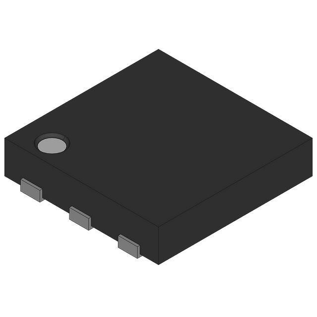
Available in XDFN6 1.6 x 1.6 mm, SOT23−5, SOT89−5 Packages
These are Pb−Free Devices
XXX
XZZ
SOT−89 5
CASE 528AB
XXXM
SOT−23−5
CASE 1212
1
XXX, XXXX = Specific Device Code
M, MM
= Date Code
ZZ
= Lot Code
Typical Applications
•
•
•
•
Battery−powered Equipment
Networking and Communication Equipment
Cameras, DVRs, STB and Camcorders
Home Appliances
NCP4623x
VIN
VIN
C1
100n
VOUT
VOUT
C2
100n
CE
GND
NCP4623xADJ
VIN
C1
100n
ORDERING INFORMATION
See detailed ordering and shipping information in the package
dimensions section on page 17 of this data sheet.
VIN
VOUT
CE
ADJ
VOUT
R1
GND
C2
100n
R2
Figure 1. Typical Application Schematics
© Semiconductor Components Industries, LLC, 2016
January, 2016 − Rev. 4
1
Publication Order Number:
NCP4623/D
�NCP4623
Thermal
Protection
Thermal
Protection
VIN
VIN
VOUT
VOUT
ADJ
Vref
Vref
Short
Protection
CE
Peak Current
Protection
CE
Short
Protection
Peak Current
Protection
GND
GND
NCP4623Hxxxxx
NCP4623HxxADJ
Figure 2. Simplified Schematic Block Diagram
PIN FUNCTION DESCRIPTION
Pin No.
XDFN
(Note 1)
Pin No.
SOT89−5
Pin No.
SOT23
Pin Name
3
1
1
VOUT
Output pin
6
2
2
GND
Ground
4
3
5
CE
Chip enable pin (Active “H”)
1
5
3
VIN
Input pin
5
4
4
NC/ADJ
2
−
−
NC
Description
No connection (non ADJ versions) / Reference Voltage of Adjustable
Output Pin (ADJ versions)
No connection
1. Tab is connected to GND. Tab should be connected to GND, but leaving it unconnected is also acceptable
www.onsemi.com
2
�NCP4623
ABSOLUTE MAXIMUM RATINGS
Rating
Symbol
Value
Unit
VIN
26.0
V
Output Voltage
VOUT
−0.3 to VIN + 0.3
V
Chip Enable Input
VCE
−0.3 to VIN + 0.3
V
Reference Input Voltage
VADJ
−0.3 to VIN + 0.3
V
Output Current
IOUT
250
mA
Input Voltage (Note 2)
Power Dissipation XDFN6−1616
640
Power Dissipation SOT89−5
900
PD
Power Dissipation SOT23−5
mW
420
Junction Temperature
TJ
−40 to 150
°C
Operation Temperature
TA
−40 to 85
°C
TSTG
−55 to 125
°C
ESD Capability, Human Body Model (Note 3)
ESDHBM
2000
V
ESD Capability, Machine Model (Note 3)
ESDMM
200
V
Storage Temperature
Stresses exceeding those listed in the Maximum Ratings table may damage the device. If any of these limits are exceeded, device functionality
should not be assumed, damage may occur and reliability may be affected.
2. Refer to ELECTRICAL CHARACTERISTIS and APPLICATION INFORMATION for Safe Operating Area.
3. This device series incorporates ESD protection and is tested by the following methods:
ESD Human Body Model tested per AEC−Q100−002 (EIA/JESD22−A114)
ESD Machine Model tested per AEC−Q100−003 (EIA/JESD22−A115)
Latchup Current Maximum Rating tested per JEDEC standard: JESD78.
Latchup Current Maximum Rating tested per JEDEC standard: JESD78.
THERMAL CHARACTERISTICS
Rating
Symbol
Value
Unit
Thermal Characteristics, XDFN6
Thermal Resistance, Junction−to−Air
RqJA
156
°C/W
Thermal Characteristics, SOT23−5
Thermal Resistance, Junction−to−Air
RqJA
238
°C/W
Thermal Characteristics, SOT89−5
Thermal Resistance, Junction−to−Air
RqJA
111
°C/W
ELECTRICAL CHARACTERISTICS NCP4623Hxxxx, CIN = COUT = 0.1 mF, TA = +25°C
Parameter
Test Conditions
Operating Input Voltage
Symbol
Min
VIN
Typ
Max
Unit
2
24
V
x0.98
x1.02
V
Output Voltage
VIN = VOUT(NOM) + 2.0 V, IOUT = 20 mA
VOUT
Output Voltage Temp. Coefficient
VIN = VOUT(NOM) + 2.0 V, IOUT = 20 mA,
−40°C ≤ TA ≤ 105ºC
DVOUT/DTA
±100
VOUT(NOM) + 1 V ≤ VIN ≤ 24 V, IOUT = 20 mA
LineReg
0.05
0.20
LoadReg
20
50
Line Regulation
Load Regulation
VIN = VOUT(NOM) +
2.0 V, IOUT = 1 mA to
40 mA
IOUT = 20 mA
Dropout Voltage
Output Current
VIN = VOUT(NOM) +
2.0 V
2.5 V ≤ VOUT ≤ 3.0 V
ppm/°C
3.1 V ≤ VOUT ≤ 5.0 V
30
75
5.1 V ≤ VOUT ≤ 12.0 V
40
115
0.20
0.40
7.1 V ≤ VOUT ≤ 10.0 V
0.25
0.50
10.1 V ≤ VOUT ≤ 12.0 V
0.30
0.55
2.5 V ≤ VOUT ≤ 7.0 V
2.5 V ≤ VOUT ≤ 2.9 V
3.0 V ≤ VOUT ≤ 12.0 V
www.onsemi.com
3
VDO
IOUT
140
150
%/V
mV
V
mA
�NCP4623
ELECTRICAL CHARACTERISTICS NCP4623Hxxxx, CIN = COUT = 0.1 mF, TA = +25°C
Parameter
Test Conditions
Symbol
Min
Typ
Max
Unit
Short Current Limit
VOUT = 0 V
ISC
45
Quiescent Current
VIN = VOUT(NOM) + 2.0 V, VCE = VIN
IQ
5
10
mA
Standby Current
VIN = 24 V, VCE = 0 V
ISTB
0.1
1.0
mA
CE Pin Threshold Voltage
CE Input Voltage “H”
VCEH
2.1
VIN
V
CE Input Voltage “L”
VCEL
0
0.3
Power Supply Rejection Ratio
VOUT = 3.3V V, VIN = 5.3 V, DVIN = 0.2 Vpk−pk,
IOUT = 30 mA, f = 1 kHz
PSRR
35
dB
Output Noise Voltage
f = 10 Hz to 100 kHz, VOUT = 3.3 V, VIN = 5.3 V,
IOUT = 30 mA
VN
90
mVrms
Thermal Shutdown Temperature
TSD
150
°C
Thermal Shutdown Release
Temperature
TSR
125
°C
mA
ELECTRICAL CHARACTERISTICS NCP4623HxxxADJ, VADJ = VOUT, CIN = COUT = 0.1 mF, TA = +25°C
Parameter
Test Conditions
Operating Input Voltage
Symbol
Min
VIN
2
2.45
Typ
2.50
Max
Unit
24
V
2.55
V
Output Voltage
VIN = VOUT(NOM) + 2.0 V, IOUT = 20 mA
VOUT
Output Voltage Temp. Coefficient
VIN = VOUT(NOM) + 2.0 V, IOUT = 20 mA,
−40°C ≤ TA ≤ 105ºC
DVOUT/DTA
±100
Line Regulation
VOUT(NOM) + 1 V ≤ VIN ≤ 24 V, IOUT = 20 mA
LineReg
0.05
0.20
%/V
Load Regulation
VIN = VOUT(NOM) + 2.0 V, IOUT = 1 mA to 40 mA
LoadReg
20
50
mV
Dropout Voltage
IOUT = 20 mA
VDO
0.20
0.40
V
Output Current
VIN = VOUT(NOM) + 2.0 V
IOUT
Short Current Limit
VOUT = 0 V
ISC
3 Quiescent Current
ppm/°C
140
mA
45
mA
VIN = VOUT(NOM) + 2.0 V, VCE = VIN
IQ
5
10
mA
Standby Current
VIN = 24 V, VCE = 0 V
ISTB
0.1
1.0
mA
CE Pin Threshold Voltage
CE Input Voltage “H”
VCEH
2.1
VIN
V
CE Input Voltage “L”
VCEL
0
0.3
VIN = 4.5 V, VOUT = 2.5 V, DVIN = 0.2 Vpk−pk,
IOUT = 30 mA, f = 1 kHz
PSRR
40
dB
f = 10 Hz to 100 kHz, VOUT = 2.5 V, VIN = 4.5 V,
IOUT = 30 mA
VN
80
mVrms
Thermal Shutdown Temperature
TSD
150
°C
Thermal Shutdown Release
Temperature
TSR
125
°C
Power Supply Rejection Ratio
Output Noise Voltage
www.onsemi.com
4
�NCP4623
TYPICAL CHARACTERISTICS
3.5
3.0
VOUT, OUTPUT VOLTAGE (V)
VOUT, OUTPUT VOLTAGE (V)
3.5
7.0 V
VIN = 4.3 V
2.5
2.0
6.0 V
1.5
5.0 V
1.0
0.5
0.0
2.5
2.0
TJ = −40°C
1.5
25°C
1.0
105°C
0.5
0.0
0
50
100
150
200
250
300
0
50
100
150
200
250
IOUT, OUTPUT CURRENT (mA)
IOUT, OUTPUT CURRENT (mA)
Figure 3. Output Voltage vs. Output Current
3.3 V Version (TJ = 255C)
Figure 4. Output Voltage vs. Output Current
3.3 V Version VIN = 5.3 V
6.0
300
6.0
VOUT, OUTPUT VOLTAGE (V)
VOUT, OUTPUT VOLTAGE (V)
3.0
5.0
4.0
3.0
VIN = 6.5 V
2.0
8.0 V
1.0
7.0 V
5.0
25°C
4.0
TJ = −40°C
3.0
2.0
1.0
105°C
6.0 V
0.0
0.0
0
50
100
150
200
250
300
0
150
200
250
Figure 5. Output Voltage vs. Output Current
5.0 V Version (TJ = 255C)
Figure 6. Output Voltage vs. Output Current
5.0 V Version VIN = 7.0 V
300
14.0
12.0
12.0
VOUT, OUTPUT VOLTAGE (V)
VOUT, OUTPUT VOLTAGE (V)
100
IOUT, OUTPUT CURRENT (mA)
14.0
15 V
VIN = 13 V
10.0
8.0
10.0
13.5 V
6.0
14 V
4.0
2.0
0.0
50
IOUT, OUTPUT CURRENT (mA)
0
50
100
150
200
250
IOUT, OUTPUT CURRENT (mA)
6.0
25°C
4.0
2.0
0.0
300
TJ = −40°C
8.0
105°C
0
50
100
150
200
250
IOUT, OUTPUT CURRENT (mA)
Figure 7. Output Voltage vs. Output Current
12.0 V Version (TJ = 255C)
Figure 8. Output Voltage vs. Output Current
12.0 V Version VIN = 14.0 V
www.onsemi.com
5
300
�NCP4623
TYPICAL CHARACTERISTICS
2.0
1.5
VDO, DROPOUT VOLTAGE (V)
VDO, DROPOUT VOLTAGE (V)
2.0
105°C
25°C
1.0
TJ = −40°C
0.5
1.5
105°C
1.0
25°C
TJ = −40°C
0.5
0.0
0.0
0
30
60
90
120
150
0
30
IOUT, OUTPUT CURRENT (mA)
Figure 9. Dropout Voltage vs. Output Current
3.3 V Version
90
120
150
Figure 10. Dropout Voltage vs. Output Current
5.0 V Version
3.35
2.0
3.34
VOUT, OUTPUT VOLTAGE (V)
VDO, DROPOUT VOLTAGE (V)
60
IOUT, OUTPUT CURRENT (mA)
1.5
1.0
25°C
105°C
0.5
TJ = −40°C
3.33
3.32
3.31
3.30
3.29
3.28
3.27
3.26
3.25
0.0
0
30
60
90
120
IOUT, OUTPUT CURRENT (mA)
−40
150
0
20
40
60
80
100
TJ, JUNCTION TEMPERATURE (°C)
Figure 11. Dropout Voltage vs. Output Current
12.0 V Version
Figure 12. Output Voltage vs. Temperature,
3.3 V Version, VIN = 5.3 V, IOUT = 20 mA
12.05
5.04
12.04
VOUT, OUTPUT VOLTAGE (V)
VOUT, OUTPUT VOLTAGE (V)
5.05
5.03
12.03
5.02
12.02
5.01
12.01
5.00
12.00
4.99
11.99
4.98
11.98
4.97
11.97
4.96
4.95
−40
−20
11.96
11.95
−20
0
20
40
60
80
100
−40
−20
0
20
40
60
80
TJ, JUNCTION TEMPERATURE (°C)
TJ, JUNCTION TEMPERATURE (°C)
Figure 13. Output Voltage vs. Temperature,
5.0 V Version, VIN = 7.0 V, IOUT = 20 mA
Figure 14. Output Voltage vs. Temperature,
12.0 V Version, VIN = 14.0 V, IOUT = 20 mA
www.onsemi.com
6
100
�NCP4623
8
8
7
7
6
6
5
5
IGND (mA)
IGND (mA)
TYPICAL CHARACTERISTICS
4
3
3
2
2
1
1
0
0
0
5
10
15
20
25
0
5
20
25
VIN, INPUT VOLTAGE (V)
Figure 16. Supply Current vs. Input Voltage,
5.0 V Version
8
7
7
6
6
5
5
4
3
4
3
2
2
1
1
0
−40
0
0
5
10
15
20
25
VIN, INPUT VOLTAGE (V)
7
7
6
6
5
5
IGND (mA)
8
4
3
1
1
40
60
40
60
80
100
3
2
20
20
4
2
0
0
Figure 18. Supply Current vs. Temperature, 3.3 V
Version, VIN = 5.3 V
8
−20
−20
TJ, JUNCTION TEMPERATURE (°C)
Figure 17. Supply Current vs. Input Voltage,
12.0 V Version
IGND (mA)
15
VIN, INPUT VOLTAGE (V)
8
0
−40
10
Figure 15. Supply Current vs. Input Voltage,
3.3 V Version
IGND (mA)
IGND (mA)
4
80
0
−40
100
−20
0
20
40
60
80
100
TJ, JUNCTION TEMPERATURE (°C)
TJ, JUNCTION TEMPERATURE (°C)
Figure 19. Supply Current vs. Temperature,
5.0 V Version, VIN = 7.0 V
Figure 20. Supply Current vs. Temperature,
12.0 V Version, VIN = 14.0 V
www.onsemi.com
7
�NCP4623
TYPICAL CHARACTERISTICS
6.0
2.5
IOUT = 40 mA
2.0
1.5
20 mA
1.0
1 mA
0.5
0.0
VOUT, OUTPUT VOLTAGE (V)
VOUT, OUTPUT VOLTAGE (V)
3.0
0
5
10
15
20
4.0
3.0
IOUT = 40 mA
2.0
20 mA
1.0
0.0
25
10
15
20
VIN, INPUT VOLTAGE (V)
Figure 22. Output Voltage vs. Input Voltage,
5.0 V Version
70
12.0
60
10.0
50
8.0
6.0
IOUT = 40 mA
4.0
5
40
IOUT = 1 mA
30
10
10
30 mA
15
20
0
0.1
25
150 mA
1
10
100
VIN, INPUT VOLTAGE (V)
FREQUENCY (kHz)
Figure 23. Output Voltage vs. Input Voltage,
12.0 V Version
Figure 24. PSRR, 3.3 V Version, VIN = 6.3 V
70
60
60
50
50
PSRR (dB)
70
IOUT = 1 mA
40
30 mA
30
25
20
20 mA
1 mA
0
5
VIN, INPUT VOLTAGE (V)
14.0
2.0
0
Figure 21. Output Voltage vs. Input Voltage,
3.3 V Version
0.0
VOUT, OUTPUT VOLTAGE (V)
5.0
1 mA
PSRR (dB)
VOUT, OUTPUT VOLTAGE (V)
3.5
1000
IOUT = 1 mA
40
30 mA
30
20
20
150 mA
10
10
150 mA
0
0.1
1
10
100
VIN, INPUT VOLTAGE (V)
1000
0
0.1
Figure 25. PSRR, 5.0 V Version, VIN = 8.0 V
1
10
FREQUENCY (kHz)
100
1000
Figure 26. PSRR, 12.0 V Version, VIN = 15.0 V
www.onsemi.com
8
�NCP4623
TYPICAL CHARACTERISTICS
7.0
16
6.0
14
12
VN (mVrms/√Hz)
4.0
3.0
2.0
10
8.0
6.0
4.0
1.0
2.0
0.1
1
10
100
0
0.01
1000
0.1
1
10
100
1000
FREQUENCY (kHz)
FREQUENCY (kHz)
Figure 27. Output Voltage Noise, 3.3 V Version,
VIN = 5.3 V, IOUT = 30 mA
Figure 28. Output Voltage Noise, 5.0 V Version,
VIN = 7.0 V, IOUT = 30 mA
45
6.0
40
5.5
35
5.0
4.5
VOUT (V)
30
25
20
15
3.1
2.9
2.7
2.5
10
2.3
5.0
2.1
0
0.01
1.9
0.1
1
10
100
0
1000
0.1
0.2
0.3
0.4
0.5
0.6
0.7
0.8
0.9
FREQUENCY (kHz)
t (ms)
Figure 29. Output Voltage Noise, 12.0 V Version,
VIN = 14.0 V, IOUT = 30 mA
Figure 30. Line Transients, 2.5 V Version,
tR = tF = 5 ms, IOUT = 30 mA
6.8
6.3
5.8
5.3
3.9
VIN (V)
VOUT (V)
VN (mVrms/√Hz)
0
0.01
VIN (V)
VN (mVrms/√Hz)
5.0
3.7
3.5
3.3
3.1
2.9
2.7
0
0.1
0.2
0.3
0.4
0.5
0.6
0.7
0.8
0.9
t (ms)
Figure 31. Line Transients, 3.3 V Version,
tR = tF = 5 ms, IOUT = 30 mA
www.onsemi.com
9
1.0
1.0
�NCP4623
TYPICAL CHARACTERISTICS
8.5
8.0
7.5
5.6
VIN (V)
VOUT (V)
7.0
5.4
5.2
5.0
4.8
4.6
4.4
0
0.1
0.2
0.3
0.4
0.5
0.6
0.7
0.8
0.9
1.0
t (ms)
Figure 32. Line Transients, 5.0 V Version,
tR = tF = 5 ms, IOUT = 30 mA
15.5
15.0
14.5
VIN (V)
VOUT (V)
14.0
12.6
12.4
12.2
12.0
11.8
11.6
11.4
0
0.1
0.2
0.3
0.4
0.5
0.6
0.7
0.8
0.9
1.0
t (ms)
Figure 33. Line Transients, 12.0 V Version,
tR = tF = 5 ms, IOUT = 30 mA
45
30
15
IOUT (mA)
VOUT (V)
0
3.1
2.9
2.7
2.5
2.3
2.1
1.9
0
0.4
0.8
1.2
1.6
2.0 2.4
t (ms)
2.8
3.2 3.6
Load Transients, 2.5 V Version, IOUT = 1 30 mA, tR = tF = 50 ms, VIN = 4.5 V
www.onsemi.com
10
4.0
�NCP4623
TYPICAL CHARACTERISTICS
45
30
15
3.9
IOUT (mA)
VOUT (V)
0
3.7
3.5
3.3
3.1
2.9
2.7
0
0.4
0.8
1.2
1.6
2.0
2.4
2.8
3.2
3.6
4.0
t (ms)
Figure 34 - Load Transients, 3.3 V Version,
IOUT = 1 - 30 mA, tR = tF = 50 ms, VIN = 5.3 V
45
30
15
IOUT (mA)
VOUT (V)
0
5.6
5.4
5.2
5.0
4.8
4.6
4.4
0
0.4
0.8
1.2
1.6
2.0 2.4
t (ms)
2.8
3.2
3.6
4.0
Figure 35. Load Transients, 5.0 V Version,
IOUT = 1 − 30 mA, tR = tF = 50 ms, VIN = 7.0 V
45
30
15
12.6
IOUT (mA)
VOUT (V)
0
12.4
12.2
12.0
11.8
11.6
11.4
0
0.4
0.8
1.2
1.6
2.0 2.4
t (ms)
2.8
3.2
3.6
Figure 36. Load Transients, 12.0 V Version,
IOUT = 1 − 30 mA, tR = tF = 50 ms, VIN = 14.0 V
www.onsemi.com
11
4.0
�NCP4623
TYPICAL CHARACTERISTICS
150
100
50
4.0
IOUT (mA)
VOUT (V)
0
3.5
3.0
2.5
2.0
1.5
1.0
0
0.4
0.8
1.2
1.6
2.0 2.4
t (ms)
2.8
3.2
3.6
4.0
Figure 37. Load Transients, 2.5 V Version,
IOUT = 1 − 100 mA, tR = tF = 50 ms, VIN = 4.5 V
150
100
50
4.8
IOUT (mA)
VOUT (V)
0
4.3
3.8
3.3
2.8
2.3
1.8
0
0.4
0.8
1.2
1.6
2.0 2.4
t (ms)
2.8
3.2
3.6
4.0
Figure 38. Load Transients, 3.3 V Version,
IOUT = 1 − 100 mA, tR = tF = 50 ms, VIN = 5.3 V
150
100
50
6.5
IOUT (mA)
VOUT (V)
0
6.0
5.5
5.0
4.5
4.0
3.5
0
0.4
0.8
1.2
1.6
2.0
2.4
2.8
3.2
3.6
t (ms)
Figure 39. Load Transients, 5.0 V Version,
IOUT = 1 − 100 mA, tR = tF = 50 ms, VIN = 7.0 V
www.onsemi.com
12
4.0
�NCP4623
TYPICAL CHARACTERISTICS
150
100
50
13.5
IOUT (mA)
VOUT (V)
0
13.0
12.5
12.0
11.5
11.0
10.5
0
0.4
0.8
1.2
1.6
2.0
2.4
2.8
3.2
3.6
4.0
t (ms)
Figure 40. Load Transients, 12.0 V Version,
IOUT = 1 − 100 mA, tR = tF = 50 ms, VIN = 14.0 V
6.75
Chip Enable
4.50
2.25
IOUT = 1 mA
VCE (V)
VOUT (V)
0
2.5
2.0
IOUT = 150 mA
1.5
1.0
0.5
IOUT = 30 mA
0
−0.5
0
0.1
0.2
0.3
0.4
0.5
0.6
0.7
0.8
0.9
1.0
t (ms)
Figure 41. Start−up, 2.5 V Version, VIN = 4.5 V
7.95
Chip Enable
5.30
2.65
VCE (V)
VOUT (V)
0
IOUT = 1 mA
4.0
3.0
2.0
IOUT = 150 mA
1.0
0
−1.0
IOUT = 30 mA
0
0.1
0.2
0.3
0.4
0.5
0.6
0.7
0.8
0.9
t (ms)
Figure 42. Start−up, 3.3 V Version, VIN = 5.3 V
www.onsemi.com
13
1.0
�NCP4623
TYPICAL CHARACTERISTICS
10.50
Chip Enable
7.00
3.50
5.0
VCE (V)
VOUT (V)
0
IOUT = 1 mA
4.0
3.0
IOUT = 150 mA
2.0
1.0
IOUT = 30 mA
0
−1.0
0
0.1
0.2
0.3
0.4
0.5
0.6
0.7
0.8
0.9
1.0
t (ms)
Figure 43. Start−up, 5.0 V Version, VIN = 7.0 V
21
Chip Enable
14
7
12.0
VCE (V)
VOUT (V)
0
IOUT = 1 mA
9.0
6.0
IOUT = 30 mA
3.0
IOUT = 150 mA
0
−3.0
0
0.1
0.2
0.3
0.4
0.5
0.6
0.7
0.8
0.9
1.0
t (ms)
Figure 45. Start−up, 12.0 V Version, VIN = 14.0 V
6.75
4.50
2.25
0
2.5
VCE (V)
VOUT (V)
Chip Enable
IOUT = 1 mA
2.0
1.5
1.0
IOUT = 30 mA
0.5
0
−0.5
IOUT = 150 mA
0
0.1
0.2
0.3
0.4
0.5
0.6
0.7
0.8
0.9
1.0
t (ms)
Figure 44. Shutdown, 2.5 V Version, VIN = 4.5 V
www.onsemi.com
14
�NCP4623
TYPICAL CHARACTERISTICS
7.95
5.30
2.65
Chip Enable
VCE (V)
VOUT (V)
0
4.0
IOUT = 1 mA
3.0
2.0
IOUT = 30 mA
1.0
0
IOUT = 150 mA
−1.0
0
0.1
0.2
0.3
0.4
0.5
0.6
0.7
0.8
0.9
1.0
t (ms)
Figure 46. Shutdown, 3.3 V Version, VIN = 5.3 V
10.5
7.0
3.5
0
5.0
4.0
VCE (V)
VOUT (V)
Chip Enable
IOUT = 1 mA
3.0
2.0
IOUT = 30 mA
1.0
0
IOUT = 150 mA
−1.0
0
0.1
0.2
0.3
0.4
0.5
0.6
0.7
0.8
0.9
1.0
t (ms)
Figure 47. Shutdown, 5.0 V Version, VIN = 7.0 V
21
14
7
0
VCE (V)
VOUT (V)
Chip Enable
IOUT = 1 mA
12.0
9.0
6.0
IOUT = 30 mA
3.0
0
−3.0
IOUT = 150 mA
0
0.1
0.2
0.3
0.4
0.5
0.6
0.7
0.8
0.9
t (ms)
Figure 48. Shutdown, 12.0 V Version,
VIN = 14.0 V
www.onsemi.com
15
1.0
�NCP4623
APPLICATION INFORMATION
of voltage divider low enough to achieve cross current
around 2 mA to eliminate error. Output voltage can be
computed from the equation:
A typical application circuits for NCP4623 series is
shown in Figure 49.
VIN
NCP4623x
VIN
C1
100n
VIN
C1
100n
ǒ
VOUT
V OUT + 2.5 1 )
VOUT
C2
100n
CE
GND
NCP4623xADJ
VIN
VOUT
CE
ADJ
GND
(eq. 1)
Enable Operation
The enable pin CE may be used for turning the regulator
on and off. The IC is switched on when a high level voltage
is applied to the CE pin. Do not leave the CE pin
unconnected or between VCEH and VCEL voltage levels as
this may leave the output voltage unstable or cause indefinite
and unexpected currents flows internally.
VOUT
R1
Ǔ
R1
) R1 @ I ADJ
R2
C2
100n
Current Limit
R2
This regulator includes a fold−back type current limit
circuit. This type of protection doesn’t limit output current
up to specified current capability in normal operation, but
when an over current occurs, output voltage and current
decrease until the over current condition ends. Typical
characteristics of this protection type can be observed in the
Output Voltage vs. Output Current graphs shown in the
typical characteristics section of this datasheet.
Figure 49. Typical Application Schematics
Input Decoupling Capacitor (C1)
A 0.1 mF ceramic input decoupling capacitor should be
connected as close as possible to the input and ground pin of
the NCP4623. Higher values and lower ESR improves line
transient response.
Thermal
As power across the IC increase, it might become
necessary to provide some thermal relief. The maximum
power dissipation supported by the device is dependent
upon board design and layout. Mounting pad configuration
on the PCB, the board material, and also the ambient
temperature affect the rate of temperature increase for the
part. When the device has good thermal conductivity
through the PCB the junction temperature will be relatively
low in high power dissipation applications.
The IC includes internal thermal shutdown circuit that
stops operation of regulator, if junction temperature is
higher than 150°C. After that, when junction temperature
decreases below 125°C, the operation of voltage regulator
will resume. During high power dissipation condition, the
regulator shuts down and resumes repeatedly protecting
itself from overheating.
Output Decoupling Capacitor (C2)
Recommended values of the ceramic output decoupling
capacitor is in the range from 0.1 mF to 2.2 mF. Stable
operation of the regulator should be achieved within this
range. If a tantalum capacitor is used, and its ESR is high,
loop oscillation may result. The capacitors should be
connected as close as possible to the output and ground pins.
Larger values and lower ESR improves dynamic
parameters.
Output Voltage Setting (ADJ version)
The output voltage of the adjustable regulator may be set
for any output voltage from its voltage reference (2.5 V) up
to VIN voltage by an external voltage divider connected
between VOUT and GND pins with its center connected to
the ADJ pin. The voltage divider is loaded by current into
ADJ pin that is typically around 200 nA. This current may
cause an error in VOUT, therefore it is good to choose values
PCB layout
Make the VIN and GND line as large as practical. If their
impedance is high, noise pickup or unstable operation may
result. Connect capacitors C1 and C2 as close as possible to
the IC, and make wiring as short as possible.
www.onsemi.com
16
�NCP4623
ORDERING INFORMATION
Nominal Output
Voltage
Description
Marking
NCP4623HSNADJT1G
Adjustable
Enable high
J24
NCP4623HSN050T1G
5.0 V
Enable high
J50
NCP4623HSN100T1G
10.0 V
Enable high
J00
NCP4623HSN120T1G
12.0 V
Enable high
J20
NCP4623HMXADJTCG
Adjustable
Enable high
BQ24
NCP4623HMX025TCG
2.5 V
Enable high
BQ25
NCP4623HMX033TCG
3.3 V
Enable high
BQ33
NCP4623HMX045TCG
4.5 V
Enable high
BQ45
NCP4623HMX048TCG
4.8 V
Enable high
BQ48
NCP4623HMX050TCG
5.0 V
Enable high
BQ50
NCP4623HMX080TCG
8.0 V
Enable high
BQ80
Device
Package
Shipping†
SOT23−5
(Pb−Free)
3000 / Tape & Reel
XDFN1616−6
(Pb−Free)
5000 / Tape & Reel
†For information on tape and reel specifications, including part orientation and tape sizes, please refer to our Tape and Reel Packaging
Specifications Brochure, BRD8011/D.
*To order other package and voltage variants, please contact your ON Semiconductor sales representative.
www.onsemi.com
17
�NCP4623
PACKAGE DIMENSIONS
XDFN6 1.6x1.6, 0.5P
CASE 711AC
ISSUE O
NOTES:
1. DIMENSIONING AND TOLERANCING PER
ASME Y14.5M, 1994.
2. CONTROLLING DIMENSION: MILLIMETERS.
3. COPLANARITY APPLIES TO THE EXPOSED
PAD AS WELL AS THE TERMINALS.
A
B
D
2X
0.05 C
PIN ONE
REFERENCE
2X
ÉÉÉ
ÉÉÉ
E
DIM
A
A1
b
D
D2
E
E2
E3
e
L
L1
0.05 C
TOP VIEW
A
0.05 C
A1
MILLIMETERS
MIN
MAX
−−−
0.40
0.00
0.05
0.15
0.25
1.60 BSC
1.25
1.35
1.60 BSC
0.65
0.75
0.15 REF
0.50 BSC
0.15
0.25
0.05 BSC
0.05 C
NOTE 3
0.05
M
D2
1
2X
RECOMMENDED
MOUNTING FOOTPRINT*
C A B
1.70
L
3
L1
3X
SEATING
PLANE
C
SIDE VIEW
E2
6X
0.05
E3
6
4
e
6X
M
PACKAGE
OUTLINE
b
0.05
M
0.77 1.79
0.38
C A B
C A B
1
0.50
PITCH
BOTTOM VIEW
6X
0.36
DIMENSIONS: MILLIMETERS
*For additional information on our Pb−Free strategy and soldering
details, please download the ON Semiconductor Soldering and
Mounting Techniques Reference Manual, SOLDERRM/D.
www.onsemi.com
18
�NCP4623
PACKAGE DIMENSIONS
SOT−89, 5 LEAD
CASE 528AB
ISSUE O
D
E
NOTES:
1. DIMENSIONING AND TOLERANCING PER ASME
Y14.5M, 1994.
2. CONTROLLING DIMENSION: MILLIMETERS.
3. LEAD THICKNESS INCLUDES LEAD FINISH.
4. DIMENSIONS D AND E DO NOT INCLUDE MOLD
FLASH, PROTRUSIONS, OR GATE BURRS.
5. DIMENSIONS L, L2, L3, L4, L5, AND H ARE MEASURED AT DATUM PLANE C.
H
DIM
A
b
b1
c
D
D2
E
e
H
L
L2
L3
L4
L5
1
TOP VIEW
c
A
0.10 C
C
SIDE VIEW
e
b1
L
1
e
b
2
RECOMMENDED
MOUNTING FOOTPRINT*
L2
4X
3
0.57
1.75
L5
5
MILLIMETERS
MIN
MAX
1.40
1.60
0.32
0.52
0.37
0.57
0.30
0.50
4.40
4.60
1.40
1.80
2.40
2.60
1.40
1.60
4.25
4.45
1.10
1.50
0.80
1.20
0.95
1.35
0.65
1.05
0.20
0.60
2.79
1.50
0.45
4
4.65
L3
L4
D2
BOTTOM VIEW
1.30
1.65
1
2X
0.62
2X
1.50
DIMENSIONS: MILLIMETERS
*For additional information on our Pb−Free strategy and soldering
details, please download the ON Semiconductor Soldering and
Mounting Techniques Reference Manual, SOLDERRM/D.
www.onsemi.com
19
�NCP4623
PACKAGE DIMENSIONS
SOT−23 5−LEAD
CASE 1212
ISSUE A
NOTES:
1. DIMENSIONING AND TOLERANCING PER
ASME Y14.5M, 1994.
2. CONTROLLING DIMENSIONS: MILLIMETERS.
3. DATUM C IS THE SEATING PLANE.
A
A
5
A2
0.05 S
B
D
A1
4
E
1
L1
2
L
3
5X
e
E1
b
0.10
C
M
C B
S
A
S
C
RECOMMENDED
SOLDERING FOOTPRINT*
3.30
DIM
A
A1
A2
b
c
D
E
E1
e
L
L1
MILLIMETERS
MIN
MAX
--1.45
0.00
0.10
1.00
1.30
0.30
0.50
0.10
0.25
2.70
3.10
2.50
3.10
1.50
1.80
0.95 BSC
0.20
--0.45
0.75
5X
0.85
5X
0.95
PITCH
0.56
DIMENSIONS: MILLIMETERS
*For additional information on our Pb−Free strategy and soldering
details, please download the ON Semiconductor Soldering and
Mounting Techniques Reference Manual, SOLDERRM/D.
ON Semiconductor and the
are registered trademarks of Semiconductor Components Industries, LLC (SCILLC) or its subsidiaries in the United States and/or other countries.
SCILLC owns the rights to a number of patents, trademarks, copyrights, trade secrets, and other intellectual property. A listing of SCILLC’s product/patent coverage may be accessed
at www.onsemi.com/site/pdf/Patent−Marking.pdf. SCILLC reserves the right to make changes without further notice to any products herein. SCILLC makes no warranty, representation
or guarantee regarding the suitability of its products for any particular purpose, nor does SCILLC assume any liability arising out of the application or use of any product or circuit, and
specifically disclaims any and all liability, including without limitation special, consequential or incidental damages. “Typical” parameters which may be provided in SCILLC data sheets
and/or specifications can and do vary in different applications and actual performance may vary over time. All operating parameters, including “Typicals” must be validated for each
customer application by customer’s technical experts. SCILLC does not convey any license under its patent rights nor the rights of others. SCILLC products are not designed, intended,
or authorized for use as components in systems intended for surgical implant into the body, or other applications intended to support or sustain life, or for any other application in which
the failure of the SCILLC product could create a situation where personal injury or death may occur. Should Buyer purchase or use SCILLC products for any such unintended or
unauthorized application, Buyer shall indemnify and hold SCILLC and its officers, employees, subsidiaries, affiliates, and distributors harmless against all claims, costs, damages, and
expenses, and reasonable attorney fees arising out of, directly or indirectly, any claim of personal injury or death associated with such unintended or unauthorized use, even if such claim
alleges that SCILLC was negligent regarding the design or manufacture of the part. SCILLC is an Equal Opportunity/Affirmative Action Employer. This literature is subject to all applicable
copyright laws and is not for resale in any manner.
PUBLICATION ORDERING INFORMATION
LITERATURE FULFILLMENT:
Literature Distribution Center for ON Semiconductor
19521 E. 32nd Pkwy, Aurora, Colorado 80011 USA
Phone: 303−675−2175 or 800−344−3860 Toll Free USA/Canada
Fax: 303−675−2176 or 800−344−3867 Toll Free USA/Canada
Email: orderlit@onsemi.com
N. American Technical Support: 800−282−9855 Toll Free
USA/Canada
Europe, Middle East and Africa Technical Support:
Phone: 421 33 790 2910
Japan Customer Focus Center
Phone: 81−3−5817−1050
www.onsemi.com
20
ON Semiconductor Website: www.onsemi.com
Order Literature: http://www.onsemi.com/orderlit
For additional information, please contact your local
Sales Representative
NCP4623/D
�