NCP508
Very Low Noise, Fast Turn
On, 50 mA Low Dropout
Voltage Regulator
Very Low Noise at 39 mVrms without a Bypass Capacitor
High Ripple Rejection of 70 dB at 1 kHz
Low Dropout Voltage of 140 mV (typ) at 30 mA
Tight Load Regulation, typically 6 mV for DIout = 50 mA
Fast Enable Turn−On time of 20 msec
Logic Level Enable
ESR can vary from a few mW to 3 W
These are Pb−Free Devices
C1
1m
ON
5
3
5
SC70−5/SC−88A/SOT−353
SQ SUFFIX
CASE 419A
xxx MG
G
1
1
X MG
G
PIN CONNECTIONS
Vout
C2
1m
2
3
X
= Specific Device Code
M = Date Code
G
= Pb−Free Package
(Note: Microdot may be in either location)
• RF Subsystems in Handsets
• Noise Sensitive Circuits; VCOs, PLL
1
12
MARKING
DIAGRAM
WDFN6
MN SUFFIX
CASE 511BJ
Typical Applications
Battery or
Unregulated
Voltage
4
5
XXX
= Specific Device Code
M
= Date Code*
G
= Pb−Free Package
(Note: Microdot may be in either location)
*Date Code orientation and/or position may
vary depending upon manufacturing location.
Features
•
•
•
•
•
•
•
•
http://onsemi.com
M
The NCP508 is a 50 mA low noise voltage regulator, designed to
exhibit fast turn on time and high ripple rejection. Each device
contains a voltage reference unit, an error amplifier, a PMOS power
transistor, resistors for setting output voltage, current limit, and
temperature limit protection circuits.
The NCP508 has been designed for use with ceramic capacitors.
The device is housed in SC−88A and WDFN6 1.5x1.5 packages.
Standard voltage versions are 1.5, 1.8, 2.5, 2.8, 3.0, and 3.3. Other
voltages are available in 100 mV steps.
Vin
1
GND
2
Enable
3
5
Vout
4
NC
4
OFF
SC−88A
(Top View)
Figure 1. Typical Application Diagram
Vout
1
6
Vin
NC
2
5
NC
GND
3
4
Enable
WDFN6
(Top View)
ORDERING INFORMATION
See detailed ordering and shipping information in the package
dimensions section on page 13 of this data sheet.
© Semiconductor Components Industries, LLC, 2011
January, 2011 − Rev. 5
1
Publication Order Number:
NCP508/D
�NCP508
PIN FUNCTION DESCRIPTION
Pin No.
Pin Name
1
Vin
Description
2
GND
3
Enable
4
N/C
Not connected pin
5
Vout
Regulated output voltage
Positive power supply input voltage
Power supply ground
This input is used to place the device into low−power stand by. When this input is pulled low, the
device is disabled. If this function is not used, Enable should be connected to Vin.
MAXIMUM RATING
Rating
Symbol
Value
Unit
Input Voltage
Vin(max)
13.0
V
Enable Voltage
Enable
−0.3 to Vin(max) + 0.3
V
Output Voltage
Vout
−0.3 to Vin(max) + 0.3
V
Power Dissipation and Thermal Characteristics (SC−88A)
Power Dissipation
Thermal Resistance, Junction−to−Ambient (Note 4)
PD
RqJA
Internally Limited
200
W
°C/W
Power Dissipation and Thermal Characteristics (WDFN6)
Power Dissipation
Thermal Resistance, Junction−to−Ambient (Note 4)
PD
RqJA
Internally Limited
313
W
°C/W
Maximum Junction Temperature
TJ
+125
°C
Operating Ambient Temperature
TA
−40 to +85
°C
Tstg
−55 to +150
°C
Tsolder
10
sec
Storage Temperature
Lead Soldering Temperature @ 260°C
Stresses exceeding Maximum Ratings may damage the device. Maximum Ratings are stress ratings only. Functional operation above the
Recommended Operating Conditions is not implied. Extended exposure to stresses above the Recommended Operating Conditions may affect
device reliability.
1. This device series contains ESD protection and exceeds the following tests:
Human Body Model 2000 V per MIL−STD−883, Method 3015.
Machine Model Method 200 V
2. Latch up Capability (85°C) $ 100 mA DC with trigger voltage
3. Maximum package power dissipation limits must be observed.
PD +
T J(max) * T A
R qJA
4. RqJA on a 30 x 30 mm PCB Cu thickness 1 oz; TA = 25°C.
RECOMMENDED OPERATING CONDITIONS
Rating
Maximum Operating Input Voltage
http://onsemi.com
2
Symbol
Max
Unit
Vin
7.0
V
�NCP508
ELECTRICAL CHARACTERISTICS (Vin = Vout(nom) + 1.0 V, Venable = Vin, Cin = 1.0 mF, Cout = 1.0 mF, TJ = 25°C, unless otherwise
noted)
Characteristic
Symbol
Min
Typ
Max
Unit
Output Voltage Tolerance (TA = 25°C, Iout = 10 mA)
Vout
−2
−
+2
%
Output Voltage Tolerance (TA = −40°C to 85°C, Iout = 10 mA)
Vout
−3
−
+3
%
Regline
−
2
20
mV
Line Regulation (Vin = Vout + 1 V to 12 V, Iout = 10 mA) (Note 5)
Load Regulation (Iout = 1.0 mA to 50 mA) (Note 5)
Regload
−
6
40
mV
Output Current (Vout = Vout(nom) – 0.1 V)
Iout(nom)
50
−
−
mA
Dropout Voltage (Vout = 3.0 V, Measured at Vout – 100 mV)
Iout = 30 mA
Iout = 40 mA
Iout = 50 mA
Vin−Vout
−
−
−
140
155
180
250
300
−
−
0.1
1
−
−
−
−
145
160
300
1100
200
260
500
1900
0.9
−
−
−
−
0.15
Quiescent Current
(Enable Input = 0V)
IQ
Ground Current
(Enable Input = Vin, Vin = Vout + 1 V, Iout = 0 mA)
(Enable Input = Vin, Iout = 1 mA)
(Enable Input = Vin, Iout = 10 mA)
(Enable Input = Vin, Iout = 50 mA)
IGND
mV
mA
mA
Enable Input Threshold Voltage
(Voltage Increasing, Output Turns On, Logic High)
(Voltage Decreasing, Output Turns Off, Logic Low)
Vth(en)
Enable Input Current (Venable = 2.4 V)
Ienable
−
8.0
15
mA
−
−
20
−
ms
Iout(max)
100
250
−
mA
Ripple Rejection (Vin = Vout(nom) + 1 Vdc + 0.5 Vpp, f = 1 kHz, Io = 10 mA)
RR
−
70
−
dB
Output Noise Voltage (f = 100 Hz to 100 kHz) (Vout = 1.5 V)
Vn
−
39
−
mVrms
Output Turn On Time (Note 6)
Output Short Circuit Current Limit (Vout = 0 V)
V
5. Low duty cycle pulse techniques are used during testing to maintain the junction temperature as close to ambient as possible.
6. Turn on time is defined from Enable at 10% to Vout at 95% nominal value. Min and max values TA = −40°C to 85°C, Tjmax = 125°C. Venable
= 0 V to Vin. Cout = 1.0 mF.
http://onsemi.com
3
�NCP508
TYPICAL CHARACTERISTICS
300
Vin−Vout, DROPOUT VOLTAGE (mV)
Vin−Vout, DROPOUT VOLTAGE (mV)
300
Vout = Vout(nom) − 0.1 V
Iload = 40 mA
250
200
150
100
50
0
−40
−20
0
20
40
60
80
100
−20
0
20
40
60
80
100
120
TEMPERATURE (°C)
3.32
Vout = Vout(nom) + 1 V
Iload = 1 mA
Vout, OUTPUT VOLTAGE (V)
Vout, OUTPUT VOLTAGE (V)
50
Figure 3. Dropout Voltage vs. Temperature,
3.3 V
1.502
1.5
1.498
1.496
1.494
1.492
−20
0
20
40
60
80
100
3.315
Vout = Vout(nom) + 1 V
Iload = 1 mA
3.31
3.305
3.3
3.295
3.29
120
−40
−20
0
20
40
60
80
100
TEMPERATURE (°C)
TEMPERATURE (°C)
Figure 4. Output Voltage vs. Temperature,
1.5 V
Figure 5. Output Voltage vs. Temperature,
3.3 V
120
250
230
Vout = Vout(nom) − 0.1 V
220
Vout = Vout(nom) − 0.1 V
Iout, OUTPUT CURRENT (mA)
Iout, OUTPUT CURRENT (mA)
100
TEMPERATURE (°C)
1.504
210
200
190
180
170
160
150
−40
150
Figure 2. Dropout Voltage vs. Temperature,
1.5 V
1.506
1.49
−40
200
0
−40
120
Vout = Vout(nom) − 0.1 V
Iload = 40 mA
250
−20
0
20
40
60
80
100
120
200
150
100
50
0
−40
−20
0
20
40
60
80
100
TEMPERATURE (°C)
TEMPERATURE (°C)
Figure 6. Output Current Limit vs.
Temperature, 1.5 V
Figure 7. Output Current Limit vs.
Temperature, 3.3 V
http://onsemi.com
4
120
�NCP508
TYPICAL CHARACTERISTICS
400
Vout = 0 V
310
Iout(max), SHORT−CIRCUIT CURRENT (mA)
Iout(max), SHORT−CIRCUIT CURRENT (mA)
330
290
270
250
230
210
190
170
150
−40
−20
0
20
40
60
80
100
250
200
150
100
50
−20
0
20
40
60
80
100
TEMPERATURE (°C)
TEMPERATURE (°C)
Figure 8. Short−Circuit Current Limit vs.
Temperature, 1.5 V
Figure 9. Short−Circuit Current Limit vs.
Temperature, 3.3 V
120
450
VEN = 0 V
IQ, QUIESCENT CURRENT (nA)
IQ, QUIESCENT CURRENT (nA)
300
0
−40
120
300
250
200
150
100
50
0
−40
−20
0
20
40
60
80
100
VEN = 0 V
400
350
300
250
200
150
100
50
0
−40
120
−20
0
20
40
60
80
100
120
TEMPERATURE (°C)
TEMPERATURE (°C)
Figure 10. Quiescent Current vs. Temperature,
1.5 V
Figure 11. Quiescent Current vs. Temperature,
3.3 V
145
146
Vin = Vout + 1 V
Iout = 0 mA
140
IGND, GROUND CURRENT (mA)
IGND, GROUND CURRENT (mA)
Vout = 0 V
350
135
130
125
120
−40
−20
0
20
40
60
80
100
120
Vin = Vout + 1 V
Iout = 0 mA
144
142
140
138
136
134
132
130
128
−40
−20
0
20
40
60
80
100
120
TEMPERATURE (°C)
TEMPERATURE (°C)
Figure 12. Ground Current vs. Temperature,
1.5 V
Figure 13. Ground Current vs. Temperature,
3.3 V
http://onsemi.com
5
�NCP508
TYPICAL CHARACTERISTICS
400
500
350
2V8,
No Load
300
3V3,
No Load
Ishort, (mA)
200
150
100
1V5,
No Load
50
0
0
1
2
3
4
5
6
VEN = Vin
Vout = 0 mA
450 Voltage Option = 1.5 V
Cin = Cout = 1 mF
TA = 25°C
400
350
300
7
8
9
250
10 11 12 13
2
3
4
5
6
7
8
9
10
11
12
Vin, INPUT VOLTAGE (V)
Vin, INPUT VOLTAGE (V)
Figure 14. Quiescent Current vs. Input Voltage
Figure 15. Output Short−Circuit Current vs.
Input Voltage
240
DROPOUT VOLTAGE (mV)
Iin, (mA)
250
VEN = Vin
Iout = 0 mA
Cin = Cout = 1 mF
TA = 25°C
Cin = Cout = 1 mF
TA = 25°C
220
200
180
160
140
2V8
120
3V
100
80
1V8
3V3
1V5
2V5
60
40
20
0
0
0.01
0.02
0.03
Iout, OUTPUT CURRENT (A)
0.04
Figure 16. Dropout Voltage vs. Output Current
http://onsemi.com
6
0.05
13
�NCP508
1.6
3.6
1.4
3.2
1.2
Vout, OUTPUT VOLTAGE (V)
Vout, OUTPUT VOLTAGE (V)
TYPICAL CHARACTERISTICS
Iout = 1.0 mA to
50 mA
1
0.8
0.6
VEN = Vin
Vout = 1.5 V
Cin = Cout = 1 mF
TA = 25°C
0.4
0.2
0
0
2
4
6
8
10
Vin, INPUT VOLTAGE (V)
2.8
2
1.6
1.2
VEN = Vin
Vout = 3.3 V
Cin = Cout = 1 mF
TA = 25°C
0.8
0.4
0
12
Iout = 1.0 mA to
50 mA
2.4
0
2
1.4
3.2
Vout, OUTPUT VOLTAGE (V)
3.6
1.2
Vin = 2.5 V
1
0.8
0.6
VEN = Vin
Vout = 1.5 V
0.2 Cin = Cout = 1 mF
TA = 25°C
0
0
0.05
0.1
0.4
0.15
0.2
0.25
Vin = 4.3 V
2.8
2.4
2
1.6
1.2
VEN = Vin
Vout = 3.3 V
Cin = Cout = 1 mF
TA = 25°C
0.8
0.4
0
0.3
0
Iout, OUTPUT CURRENT (A)
0.05
0.1
14
12
Region of Instability
8
Region of Stability
4
Cin = Cout = 1 mF
TA = 25°C
2
0
0
5
10
15
0.2
0.25
Figure 20. Output Voltage vs. Output Current
16
6
0.15
Iout, OUTPUT CURRENT (A)
Figure 19. Output Voltage vs. Output Current
10
12
Figure 18. Output Voltage vs. Input Voltage
1.6
ESR, EQUIVALENT SERIES RESISTANCE (W)
Vout, OUTPUT VOLTAGE (V)
Figure 17. Output Voltage vs. Input Voltage
4
6
8
10
Vin, INPUT VOLTAGE (V)
20
25
30
35
40
45
Iout, OUTPUT CURRENT (mA)
Figure 21. Equivalent Series Resistance vs.
Output Current, X7R, MLCC Capacitor
http://onsemi.com
7
50
0.3
�NCP508
TYPICAL CHARACTERISTICS
Input Voltage (V)
3.5
2.5
Vout = 1.5 V
Vin = 2.5 V to 3.5 V /rate 1 V/ms
Iload = 40 mA
Cout = 1 mF MLCC
Load Current (mA)
20 mV
10 mV
60 mV
30 mV
Vout = 1.5 V
Vin = 2.5 V
Iload = 1 to 50 mA
Cout = 1 uF MLCC
Output Voltage Deviation (mV)
0
0
−10 mV
−30 mV
−20 mV
−60 mV
Output Voltage Deviation (mV)
−30 mV
Figure 22. Line Transient Response
1.5 V/40 mA
Figure 23. Load Transient Response 1.5 V
Input voltage (V)
3.5
2.5
20 mV
10 mV
Vout = 1.5 V
Vin = 2.5 V to 3.5 V /rate 1 V/ms
Iload = 50 mA
Cout = 4.7 mF MLCC
Output Voltage Deviation (mV)
0
−10 mV
−20 mV
Figure 24. Line Transient Response
1.5 V/50 mA
http://onsemi.com
8
�NCP508
TYPICAL CHARACTERISTICS
Load Current (mA)
Vout = 3.3 V
Vin = 4.3 V
Iload = 1 to 40 mA
Cout = 1 mF MLCC
Input Voltage (V)
5.3
Vout = 3.3 V
Vin = 4.3 V to 5.3 V /rate 1 V/ms
Iload = 40 mA
Cout = 1 mF MLCC
4.3
20 mV
10 mV
0
Output Voltage Deviation (mV)
40 mV
−10 mV
20 mV
−20 mV
0
Output Voltage Deviation (mV)
−20 mV
−30 mV
−40 mV
Figure 25. Load Transient Response 3.3 V
Figure 26. Line Transient Response
3.3 V/40 mA
Input Voltage (V)
5.3
4.3
Vout = 3.3 V
Vin = 4.3 V to 5.3 V /rate 1 V/ms
Iload = 50 mA
Cout = 4.7 mF MLCC
20 mV
Output Voltage Deviation (mV)
10 mV
0
−10 mV
−20 mV
Figure 27. Line Transient Response
3.3 V/50 mA
http://onsemi.com
9
�NCP508
TYPICAL CHARACTERISTICS
3.0E−07
2.5E−07
(nV/√HZ)
2.0E−07
1.5E−07
1.0E−07
RMS Noise Value (100 Hz − 100 kHz) = 39 mV
0.5E−07
0.0
10
100
1000
10000
100000
1000000
FREQUENCY (Hz)
Figure 28. Output Voltage Noise
Vout = 1.5 V, Iout = 40 mA
RR, RIPPLE REJECTION (dB)
90
80
70
60
50
1.5 V
2.5 V
3.3 V
40
30
20
10
0
10
100
1000
10000
100000
1000000
fripple, RIPPLE FREQUENCY (Hz)
Figure 29. Ripple Rejection vs. Frequency
Iout = 40 mA, 0.5 Vpp
Iout = No Load
Cin = Cout = 1 mF
Vin = VEN = 2.8 V
Vout = 1.8 V
TA = 25°C
Iout = 50 mA
Cin = Cout = 1 mF
Vin = VEN = 2.8 V
Vout = 1.8 V
TA = 25°C
Vin = VEN
Vout
Vin = VEN
Vout
Iin
Iin
Figure 30. Startup, No Load
Figure 31. Startup, Iout = 50 mA
http://onsemi.com
10
�NCP508
0.06
Iout, OUTPUT CURRENT (A)
Cin = Cout = 1 mF
Vin = VEN = 2.8 V
Vout = 2.5 V
TA = 25°C
Ilimit = 180 mA
50 mA/div
0.05
0.04
0.03
0.02
VEN = Vin
Cin = Cout = 1 mF
TA = 85°C
0.01
500 ms/div
0
0
1
2
3
4
5
6
7
8
9
10 11 12 13
Vin, INPUT VOLTAGE (V)
Figure 33. Measured Power Operating Area,
1.5 V, TA = 855C, Vout_drop = max 0.1 V
Figure 32. Hard Short−Circuit Current (by Copper Wires)
350
0.25
0.2
PD
qJA (°C/W)
250
200
qJA
150
0.15
0.1
100
0.05
50
33 x 26 mm
0
PCB Copper Thickness = 1.0 oz
0
100 200 300 400 500 600 700 800 900 1000
0
COPPER HEAT SPREADER AREA (mm2)
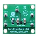
Figure 34. Evaluation Board
Figure 35. SC70−5 Thermal Resistance vs.
Copper Heat Spreader Area
400
350
qJA (°C/W)
300
250
200
150
100
50
PCB Copper Thickness = 1.0 oz
0
100
200
300
400
500
600
700
800
900
PCB COPPER HEAT SPREADER AREA (mm2)
Figure 36. WDFN6 Thermal Resistance vs.
Copper Heat Spreader Area
http://onsemi.com
11
MAX POWER DISSIPATION (W)
300
�NCP508
DEFINITIONS
Load Regulation
Line Regulation
The change in output voltage for a change in output
current at a constant temperature.
The change in output voltage for a change in input voltage.
The measurement is made under conditions of low
dissipation or by using pulse technique such that the average
chip temperature is not significantly affected.
Dropout Voltage
The input/output differential at which the regulator output
no longer maintains regulation against further reductions in
input voltage. Measured when the output drops 100 mV
below its nominal. The junction temperature, load current,
and minimum input supply requirements affect the dropout
level.
Line Transient Response
Typical over and undershoot response when input voltage
is excited with a given slope.
Thermal Protection
Internal thermal shutdown circuitry is provided to protect
the integrated circuit in the event that the maximum junction
temperature is exceeded. When activated at typically 125°C,
the regulator turns off. This feature is provided to prevent
failures from accidental overheating.
Maximum Power Dissipation
The maximum total dissipation for which the regulator
will operate within its specifications.
Quiescent Current
The quiescent current is the current which flows through
the ground when the LDO operates without a load on its
output: internal IC operation, bias, etc. When the LDO
becomes loaded, this term is called the Ground current. It is
actually the difference between the input current (measured
through the LDO input pin) and the output current.
Maximum Package Power Dissipation
The maximum power package dissipation is the power
dissipation level at which the junction temperature reaches
its maximum operating value, i.e. 150°C. Depending on the
ambient power dissipation and thus the maximum available
output current.
APPLICATIONS INFORMATION
Hints
Typical application circuit for the NCP508 series is shown
in Figure 1.
Please be sure the Vin and GND lines are sufficiently wide.
When the impedance of these lines is high, there is a chance
to pick up noise or cause the regulator to malfunction.
Set external components, especially the output capacitor,
as close as possible to the circuit, and make leads as short as
possible.
Input Decoupling (C1)
An input capacitor of at least 1.0 mF,(ceramic or tantalum)
is recommended to improve the transient response of the
regulator and/or if the regulator is located more than a few
inches from the power source. It will also reduce the circuit’s
sensitivity to the input line impedance at high frequencies.
The capacitor should be mounted with the shortest possible
track length directly across the regular’s input terminals.
Higher values and lower ESR will improve the overall line
transient response.
Thermal Considerations
Internal thermal limiting circuitry is provided to protect
the integrated circuit in the event that the maximum junction
temperature is exceeded.
The maximum power dissipation supported by the device
is dependent upon board design and layout. Mounting pad
configuration on the PCB, the board material and also the
ambient temperature effect the rate of temperature rise for
the part. This is stating that when the NCP508 has good
thermal conductivity through the PCB, the junction
temperature will be relatively low with high power
dissipation applications.
The maximum dissipation the package can handle is given
by:
Output Decoupling (C2)
The NCP508 is a stable regulator and does not require a
minimum output current. Capacitors exhibiting ESRs
ranging from a few mW up to 3 W can safely be used. The
minimum decoupling value is 1.0 mF and can be augmented
to fulfill stringent load transient requirements. The regulator
accepts ceramic chip capacitors as well as tantalum devices.
Larger values improve noise rejection and load regulation
transient response.
PD +
Enable Operation
The enable pin will turn on or off the regulator. The limits
of threshold are covered in the electrical specification
section of this datasheet. If the enable is not used then the pin
should be connected to Vin.
T J(max) * T A
R qJA
(eq. 1)
where:
− TJ{max) is the maximum allowable junction temperature
of the die, which is 150°C
− TA is the ambient operating temperature
− Rqja is dependent on the surrounding PCB layout
http://onsemi.com
12
�NCP508
ORDERING INFORMATION
Nominal Output Voltage
Marking
Package
Shipping†
NCP508SQ15T1G
1.5
D5A
SC−88A
(Pb−Free)
3000 / Tape & Reel
NCP508SQ18T1G
1.8
D5C
SC−88A
(Pb−Free)
3000 / Tape & Reel
NCP508SQ25T1G
2.5
D5D
SC−88A
(Pb−Free)
3000 / Tape & Reel
NCP508SQ28T1G
2.8
D5E
SC−88A
(Pb−Free)
3000 / Tape & Reel
NCP508SQ30T1G
3.0
D5F
SC−88A
(Pb−Free)
3000 / Tape & Reel
NCP508SQ33T1G
3.3
D5G
SC−88A
(Pb−Free)
3000 / Tape & Reel
NCP508MT15TBG
1.5
B
WDFN6
(Pb−Free)
3000 / Tape & Reel
NCP508MT18TBG
1.8
A
WDFN6
(Pb−Free)
3000 / Tape & Reel
NCP508MT25TBG
2.5
C
WDFN6
(Pb−Free)
3000 / Tape & Reel
NCP508MT28TBG
2.8
D
WDFN6
(Pb−Free)
3000 / Tape & Reel
NCP508MT30TBG
3.0
E
WDFN6
(Pb−Free)
3000 / Tape & Reel
NCP508MT33TBG
3.3
F
WDFN6
(Pb−Free)
3000 / Tape & Reel
Device
†For information on tape and reel specifications, including part orientation and tape sizes, please refer to our Tape and Reel Packaging
Specifications Brochure, BRD8011/D.
NOTE: Additional voltages in 100 mV steps are available upon request by contacting your ON Semiconductor representative.
http://onsemi.com
13
�MECHANICAL CASE OUTLINE
PACKAGE DIMENSIONS
SC−88A (SC−70−5/SOT−353)
CASE 419A−02
ISSUE L
SCALE 2:1
A
NOTES:
1. DIMENSIONING AND TOLERANCING
PER ANSI Y14.5M, 1982.
2. CONTROLLING DIMENSION: INCH.
3. 419A−01 OBSOLETE. NEW STANDARD
419A−02.
4. DIMENSIONS A AND B DO NOT INCLUDE
MOLD FLASH, PROTRUSIONS, OR GATE
BURRS.
G
5
4
−B−
S
1
2
DATE 17 JAN 2013
DIM
A
B
C
D
G
H
J
K
N
S
3
D 5 PL
0.2 (0.008)
B
M
M
N
INCHES
MIN
MAX
0.071
0.087
0.045
0.053
0.031
0.043
0.004
0.012
0.026 BSC
--0.004
0.004
0.010
0.004
0.012
0.008 REF
0.079
0.087
MILLIMETERS
MIN
MAX
1.80
2.20
1.15
1.35
0.80
1.10
0.10
0.30
0.65 BSC
--0.10
0.10
0.25
0.10
0.30
0.20 REF
2.00
2.20
J
GENERIC MARKING
DIAGRAM*
C
K
H
XXXMG
G
SOLDER FOOTPRINT
0.50
0.0197
XXX = Specific Device Code
M
= Date Code
G
= Pb−Free Package
0.65
0.025
0.65
0.025
0.40
0.0157
1.9
0.0748
SCALE 20:1
(Note: Microdot may be in either location)
*This information is generic. Please refer to
device data sheet for actual part marking.
Pb−Free indicator, “G” or microdot “G”, may
or may not be present. Some products may
not follow the Generic Marking.
mm Ǔ
ǒinches
STYLE 1:
PIN 1. BASE
2. EMITTER
3. BASE
4. COLLECTOR
5. COLLECTOR
STYLE 2:
PIN 1. ANODE
2. EMITTER
3. BASE
4. COLLECTOR
5. CATHODE
STYLE 3:
PIN 1. ANODE 1
2. N/C
3. ANODE 2
4. CATHODE 2
5. CATHODE 1
STYLE 4:
PIN 1. SOURCE 1
2. DRAIN 1/2
3. SOURCE 1
4. GATE 1
5. GATE 2
STYLE 6:
PIN 1. EMITTER 2
2. BASE 2
3. EMITTER 1
4. COLLECTOR
5. COLLECTOR 2/BASE 1
STYLE 7:
PIN 1. BASE
2. EMITTER
3. BASE
4. COLLECTOR
5. COLLECTOR
STYLE 8:
PIN 1. CATHODE
2. COLLECTOR
3. N/C
4. BASE
5. EMITTER
STYLE 9:
PIN 1. ANODE
2. CATHODE
3. ANODE
4. ANODE
5. ANODE
DOCUMENT NUMBER:
DESCRIPTION:
98ASB42984B
STYLE 5:
PIN 1. CATHODE
2. COMMON ANODE
3. CATHODE 2
4. CATHODE 3
5. CATHODE 4
Note: Please refer to datasheet for
style callout. If style type is not called
out in the datasheet refer to the device
datasheet pinout or pin assignment.
Electronic versions are uncontrolled except when accessed directly from the Document Repository.
Printed versions are uncontrolled except when stamped “CONTROLLED COPY” in red.
SC−88A (SC−70−5/SOT−353)
PAGE 1 OF 1
ON Semiconductor and
are trademarks of Semiconductor Components Industries, LLC dba ON Semiconductor or its subsidiaries in the United States and/or other countries.
ON Semiconductor reserves the right to make changes without further notice to any products herein. ON Semiconductor makes no warranty, representation or guarantee regarding
the suitability of its products for any particular purpose, nor does ON Semiconductor assume any liability arising out of the application or use of any product or circuit, and specifically
disclaims any and all liability, including without limitation special, consequential or incidental damages. ON Semiconductor does not convey any license under its patent rights nor the
rights of others.
© Semiconductor Components Industries, LLC, 2018
www.onsemi.com
�MECHANICAL CASE OUTLINE
PACKAGE DIMENSIONS
WDFN6 1.5x1.5, 0.5P
CASE 511BJ
ISSUE C
DATE 06 OCT 2015
SCALE 4:1
D
L
A
B
NOTES:
1. DIMENSIONING AND TOLERANCING PER
ASME Y14.5M, 1994.
2. CONTROLLING DIMENSION: MILLIMETERS.
3. DIMENSION b APPLIES TO PLATED
TERMINAL AND IS MEASURED BETWEEN
0.15 AND 0.30mm FROM TERMINAL TIP.
4. COPLANARITY APPLIES TO THE EXPOSED
PAD AS WELL AS THE TERMINALS.
L1
DETAIL A
ÍÍÍÍ
ÍÍÍÍ
ÍÍÍÍ
ALTERNATE TERMINAL
CONSTRUCTIONS
E
PIN ONE
REFERENCE
ÉÉÉ
ÉÉÉ
EXPOSED Cu
0.10 C
2X
2X
0.10 C
0.05 C
TOP VIEW
DETAIL B
A3
MOLD CMPD
ÉÉ
ÉÉ
ÇÇ
DIM
A
A1
A3
b
D
E
e
L
L1
L2
A3
A1
DETAIL B
ALTERNATE
CONSTRUCTIONS
GENERIC
MARKING DIAGRAM*
A
0.05 C
1
A1
NOTE 4
C
SIDE VIEW
DETAIL A
e
1
SEATING
PLANE
XXM
G
XX = Specific Device Code
M = Date Code
G
= Pb−Free Package
5X
L
3
MILLIMETERS
MIN
MAX
0.70
0.80
0.00
0.05
0.20 REF
0.20
0.30
1.50 BSC
1.50 BSC
0.50 BSC
0.40
0.60
--0.15
0.50
0.70
*This information is generic. Please refer to
device data sheet for actual part marking.
Pb−Free indicator, “G” or microdot “ G”,
may or may not be present.
L2
RECOMMENDED
MOUNTING FOOTPRINT*
6
4
6X
b
0.10 C A
BOTTOM VIEW
0.05 C
B
6X
0.35
5X
0.73
NOTE 3
1.80
0.83
0.50
PITCH
DIMENSIONS: MILLIMETERS
*For additional information on our Pb−Free strategy and soldering
details, please download the ON Semiconductor Soldering and
Mounting Techniques Reference Manual, SOLDERRM/D.
DOCUMENT NUMBER:
DESCRIPTION:
98AON50296E
WDFN6, 1.5 X 1.5, 0.5 P
Electronic versions are uncontrolled except when accessed directly from the Document Repository.
Printed versions are uncontrolled except when stamped “CONTROLLED COPY” in red.
PAGE 1 OF 1
ON Semiconductor and
are trademarks of Semiconductor Components Industries, LLC dba ON Semiconductor or its subsidiaries in the United States and/or other countries.
ON Semiconductor reserves the right to make changes without further notice to any products herein. ON Semiconductor makes no warranty, representation or guarantee regarding
the suitability of its products for any particular purpose, nor does ON Semiconductor assume any liability arising out of the application or use of any product or circuit, and specifically
disclaims any and all liability, including without limitation special, consequential or incidental damages. ON Semiconductor does not convey any license under its patent rights nor the
rights of others.
© Semiconductor Components Industries, LLC, 2019
www.onsemi.com
�onsemi,
, and other names, marks, and brands are registered and/or common law trademarks of Semiconductor Components Industries, LLC dba “onsemi” or its affiliates
and/or subsidiaries in the United States and/or other countries. onsemi owns the rights to a number of patents, trademarks, copyrights, trade secrets, and other intellectual property.
A listing of onsemi’s product/patent coverage may be accessed at www.onsemi.com/site/pdf/Patent−Marking.pdf. onsemi reserves the right to make changes at any time to any
products or information herein, without notice. The information herein is provided “as−is” and onsemi makes no warranty, representation or guarantee regarding the accuracy of the
information, product features, availability, functionality, or suitability of its products for any particular purpose, nor does onsemi assume any liability arising out of the application or use
of any product or circuit, and specifically disclaims any and all liability, including without limitation special, consequential or incidental damages. Buyer is responsible for its products
and applications using onsemi products, including compliance with all laws, regulations and safety requirements or standards, regardless of any support or applications information
provided by onsemi. “Typical” parameters which may be provided in onsemi data sheets and/or specifications can and do vary in different applications and actual performance may
vary over time. All operating parameters, including “Typicals” must be validated for each customer application by customer’s technical experts. onsemi does not convey any license
under any of its intellectual property rights nor the rights of others. onsemi products are not designed, intended, or authorized for use as a critical component in life support systems
or any FDA Class 3 medical devices or medical devices with a same or similar classification in a foreign jurisdiction or any devices intended for implantation in the human body. Should
Buyer purchase or use onsemi products for any such unintended or unauthorized application, Buyer shall indemnify and hold onsemi and its officers, employees, subsidiaries, affiliates,
and distributors harmless against all claims, costs, damages, and expenses, and reasonable attorney fees arising out of, directly or indirectly, any claim of personal injury or death
associated with such unintended or unauthorized use, even if such claim alleges that onsemi was negligent regarding the design or manufacture of the part. onsemi is an Equal
Opportunity/Affirmative Action Employer. This literature is subject to all applicable copyright laws and is not for resale in any manner.
PUBLICATION ORDERING INFORMATION
LITERATURE FULFILLMENT:
Email Requests to: orderlit@onsemi.com
onsemi Website: www.onsemi.com
◊
TECHNICAL SUPPORT
North American Technical Support:
Voice Mail: 1 800−282−9855 Toll Free USA/Canada
Phone: 011 421 33 790 2910
Europe, Middle East and Africa Technical Support:
Phone: 00421 33 790 2910
For additional information, please contact your local Sales Representative
�