NCP5215 Dual Synchronous Buck Controller for Notebook Power System
The NCP5215, a high−efficiency and fast−transient−response dual−channel buck controller, provides a multifunctional power solution for notebook power system. 180o interleaved operation function between the two channels has capabilities of reducing the common input capacitor requirement and improving noise immunity. Adaptive −Voltage −Positioning (AVP) control reduces the requirement of output filter capacitors. Programmable power−saving operation ensures high efficiency over entire load range. Input feedforward voltage−mode control is employed to deal with wide input voltage range. Transient−Response−Enhancement (TRE) control for the both channels enables fast transient response.
Features http://onsemi.com MARKING DIAGRAM
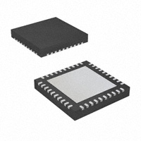
QFN40 MN SUFFIX CASE 488AR 1 40 A WL YY WW G = Assembly Location = Wafer Lot = Year = Work Week = Pb−Free Package
NCP5215 AWLYYWWG
• Wide Input Voltage Range: 4.5 V to 24 V • Adjustable Output Voltage Range: 0.8 V to 3.0 V • Selectable Nominal Fixed Switching Frequency: • • • • • • • • • • • • • • • •
200 kHz, 300 kHz, and 400 kHz 180° Interleaved Operation Function between the Two Channels Programmable Adaptive−Voltage−Positioning (AVP) Operation Programmable Transient−Response−Enhancement (TRE) Control Power Saving Operation under Light Load Condition Input Feedforward Voltage Mode Control Resistive or Inductor’s DCR Current Sensing 1% Internal 0.8 V Reference External Soft−Start Operation Output Discharge and Soft−Stop Built−in Gate Drivers Input Supplies Undervoltage Lockout Output Overvoltage and Undervoltage Protections Accurate Overcurrent Protection Thermal Shutdown Protection QFN40 Package This is a Pb−Free Device
PIN CONNECTIONS
34 CS1−/Vo1 40 TRESET1 39 COMP1 36 VDRP1
32 SWN1
35 ILMT1
33 CS1+
38 INV1
FSET VCC AGND VREF PGOOD1 PGOOD2 EN1 EN2 SS1
31 TG1 30 BST1 29 VCCP1 28 BG1 27 PGND1 26 VIN 25 FPWM# 24 PGND2 23 BG2 22 VCCP2 21 BST2 TG2 20
1 2 3 4 5 6 7 8 9
SS2 10 COMP2 12 INV2 13 FB2 14 VDRP2 15 ILIM2 16 CS2−/Vo2 17 CS2+ 18 TRESET2 11 SWN2 19
Typical Applications
• Notebook Computers • CPU Chipset Power Supplies
ORDERING INFORMATION
Device NCP5215MNR2G Package QFN40 (Pb−Free) Shipping 2500/T ape & Reel
†For information on tape and reel specifications, including part orientation and tape sizes, please refer to our Tape and Reel Packaging Specification Brochure, BRD8011/D.
37 FB1
NCP5215
(Top View)
© Semiconductor Components Industries, LLC, 2008
October, 2008 − Rev. 5
1
Publication Order Number: NCP5215/D
�NCP5215
TRESET1 40
TRE1
5VCC
Vin
CS1+
33 30 DSCH1 FB1 CDIFF1 CCM1
BST1 TG1 SWN1 5VCC Vo1 CS1+ CS1−
CS1−/Vo1 34
12 Ohm
RAMP GENERATOR & PWM LOGIC 1
PWM1
GATE DRIVER
LSEN1
31 32
Vo1
FB1
37
1
29 28 27
VCCP1 BG1
INV1 VREF VDRP1 COMP1
38 36 39 VREF
COMP1
SWN1
PGND1
OVP1 CLK CLK1 VIN FPWM Soft Start 1 CDIFF1 Over Current Detector 1 OC1 THERMAL SHUTDOWN VCC Vin TSD FB1 EN1
EN_DRV1 VREF
SS1 EN1 ILIM1 FPWM 5VCC
9 7 35 25
VREF
VCC FSET AGND VREF
2 1 3 4 26 5 6 CLK CLK2 VIN FPWM 0.8V OSC Digital Counter & 180o Phase Shift
OC1
5VCC PROTECTION and CONTROL LOGIC
Vin
NCP5215
DSCH1 PGOOD1 FB2 EN2 OC2 DSCH2 PGOOD2
Vin VIN PGOOD1 PGOOD2
TRESET2
OVP2
EN_DRV2 5VCC Vin
11
TRE2
CS2+
18
CS2−/Vo2 17
12 Ohm
21
BST2 TG2 SWN2 5VCC Vo2 CS2+ CS2−
DSCH2 FB2 CDIFF2 CCM2
RAMP GENERATOR & PWM LOGIC 2
PWM2
20
GATE DRIVER
LSEN2 19
Vo2
FB2
14
2
22 23
VCCP2 BG2
INV2 VREF VDRP2 COMP2
13 15 12 VREF
COMP2
SWN2 24
PGND2
SS2 EN2 ILIM2
10 8 16 CDIFF2
Soft Start 2
VREF
Over Current Detector 2
OC2
Figure 1. Internal Block Diagram and Typical Application
http://onsemi.com
2
�NCP5215
PIN FUNCTION DESCRIPTION
Pin No. 1 2 3 4 5 6 7 8 9 10 11 12 13 14 15 16 17 18 19 20 21 22 23 24 25 26 27 28 29 30 31 32 33 34 35 36 37 38 39 40 Symbol FSET VCC AGND VREF PGOOD1 PGOOD2 EN1 EN2 SS1 SS2 TRESET2 COMP2 INV2 FB2 VDRP2 ILMT2 CS2− / Vo2 CS2+ SWN2 TG2 BST2 VCCP2 BG2 PGND2 FPWM# Vin PGND1 BG1 VCCP1 BST1 TG1 SWN1 CS1+ CS1− / Vo1 ILMT1 VDRP1 FB1 INV1 COMP1 TRESET1 VCC This pin powers the control section of IC. Analog Ground Low noise ground for control section of IC. Reference Voltage Output Internal 0.8 V reference output. Power GOOD 1 Power good indicator of the output voltage of Channel 1. (Open drained) Power GOOD 2 Power good indicator of the output voltage of Channel 2. (Open drained) Enable 1 Enable logic input of Channel 1. Enable 2 Enable logic input of Channel 2. Soft−Start 1 Soft−starting programmable pin of Channel 1. Soft Start 2 Soft−starting programmable pin of Channel 2. Transient Response Enhancement SET 2 Channel 2 Transient−Response−Enhancement (TRE) programmable pin. COMP2 Output of the error amplifier of Channel 2. Inverting Input 2 Error amplifier’s inverting input pin of Channel 2. Feedback 2 Output voltage feedback of Channel 2. Voltage Droop 2 Channel 2 voltage droop output to the compensation. This pin is used to program the adaptive−voltage−position (AVP) function for Channel 2. Current Limit 2 Current limit programmable pin of Channel 2. Current Sense 2− Channel 2 inductor current differential sense inverting input. Current Sense 2+ Channel 2 inductor current differential sense non−inverting input. Switch Node 2 Switch node between the top MOSFET and bottom MOSFET of Channel 2. Top Gate 2 Gate driver output of the top N−Channel MOSFET for Channel 2. BOOTSTRAP Connection 2 Channel 2 top gate driver input supply, a bootstrap capacitor connection between SWN2 and this pin. VCC Power 2 This pin powers the bottom gate driver of Channel 2. Bottom Gate 2 Gate driver output of the bottom N−Channel MOSFET for Channel 2. Power Ground 2 Ground reference and high−current return path for the bottom gate driver of Channel 2. Forced PWM Forced PWM enable logic input. Low to enable forced PWM mode and disable power−saving mode for both channels. Vin Input voltage monitor input. Power Ground 1 Ground reference and high−current return path for the bottom gate driver of Channel 1. Bottom Gate 1 Gate driver output of the bottom N−Channel MOSFET for Channel 1. VCC Power 1 This pin powers the bottom gate driver of Channel 1. BOOTSTRAP Connection 1 Channel 1 top gate driver input supply, a bootstrap capacitor connection between SWN1 and this pin. Top Gate 1 Gate driver output of the top N−Channel MOSFET for Channel 1. Switch Node 1 Switch node between the top MOSFET and bottom MOSFET of Channel 1. Current Sense 1+ Channel 1 inductor current differential sense non−inverting input. Current Sense 1− Channel 1 inductor current differential sense inverting input. Current Limit 1 Current limit programmable pin of Channel 1. Voltage Droop 1 Channel 1 voltage droop output to the compensation. This pin is used to program the Adaptive−Voltage−Position (AVP) function for Channel 1. Feedback 1 Output voltage feedback of Channel 1. Inverting Input 1 Error amplifier’s inverting input pin of Channel 1. COMP1 Output of the error amplifier of Channel 1. Transient Response Enhancement SET 1 Channel 1 Transient−Response−Enhancement (TRE) program pin. Description Frequency SET Programmable pin of switching frequency for two channels.
http://onsemi.com
3
�NCP5215
MAXIMUM RATINGS
Rating Power Supply Voltages to AGND High−Side Gate Driver Supplies: BST1 to SWN1, BST2 to SWN2 High−Side FET Gate Driver Voltages: TG1 to SWN1, TG2 to SWN2 Symbol VCC, VCCP1, VCCP2 VBST1 − VSWN1, VBST2 − VSWN2, VTG1 − VSWN1, VTG2 − VSWN2, Vin VSWN1, VSWN2 VGND RqJA TJ TA Tstg MSL Value −0.3, 6.0 −0.3, 6.0 Unit V V
Input Voltage Sense Inputs to AGND Switch Nodes PGND1, PGND2 to AGND Thermal Characteristics Thermal Resistance, Junction−to−Air (Pad soldered to PCB) Operating Junction Temperature Range Operating Ambient Temperature Range Storage Temperature Range Moisture Sensitivity Level
−0.3, 27 −4.0 ( 4.25V ? & VIN > 4.0V ? & ENBL= HIGH ?
Re−apply VCC or VIN or ENBL
yes no & no OV
Vo Discharge Mode
Vo < 0.3V
TG Latch Off BG Latch On
yes VCC < 4.0V or VIN < 3.5V or ENBL = LOW
OV
OVP
OV Soft Start and Normal Operation
OC
UV
OCP
TG & BG Latch Off
UVP
Vo Discharge Mode
Figure 34. State Diagram per Channel
http://onsemi.com
17
�NCP5215
Vin NTMS4705N NTMS4705N NTMS4705N
M1 Vo1 1.5V / 5A Co11 Co1 L1 2.2uH 3.6k Rs1
M2 L2 1.5uH 4.3k Rs2 Vo2 1.05V/6A Cs2 Co2 Co21
Cin1 10uF Rif
Cin2 10uF 15nF 20
Cs1
M3
NTMS4705N
M4
Cif
10uF 220uF
0.1uF
0.1uF
220uF*2 10uF
PGND 5VCC Db1 BAT54WT1 Cb1 0.1uF 31 TG1 Cpf1 1uF
PGND FPWM# Cpf2 1uF 5VCC Db2 BAT54WT1 Cb2 0.1uF TG2 20 SWN2 19 CS2+ 18 CS2−/Vo2 17 NCP5215MNR2G ILIM2 16 VDRP2 15 FB2 14 INV2 13 COMP2 12 PGOOD1 PGOOD2 AGND VREF TRESET2 11 EN1 EN2 SS1 SS2 VCC 36k
PGND
30 29 28 27 26 25 24 23 22 21 PGND1 VIN FPWM# PGND2 BG1 BST1 BG2 VCCP1 VCCP2 BST2
32 SWN1 VREF Ril11 100k Rdp1 2k Ril12 82k Cdp1 47pF R11 C13 R13 1nF 750 R14 11k 10k 33 CS1+ 34 CS1−/Vo1 35 ILIM1 36 VDRP1 37 FB1 38 INV1 39 COMP1 FSET 40 TRESET1
VREF Ril22 36k Cdp2 47pF R21 820pF 910 220pF 200k R24 R23 C22 R22 C23 13k Ril21 100k Rdp2 3k
R12
75k
5VCC 68pF C11 390k Rt1
68pF
220pF
PGOOD1
PGOOD2
C12
EN1
PGND
Figure 35. Typical Application Schematic Diagram
http://onsemi.com
18
EN2
1uF
1uF
4.7nF
Rt2
20
200k
Ccf
4.7nF
Css1
Cref
Css2
C21
Rcf
1
2
3
4
5
6
7
8
9
10
�NCP5215
Table 2. BILL OF MATERIALS FOR THE TYPICAL APPLICATION
Item 1 2 3 4 PCS 1 4 2 2 Part Reference IC1 M1, M2, M3, M4 Db1, Db2 Cdp1, Cdp2 C11, C22 NCP5215 Power MOSFET 30 V, 12 A, Single N−Channel SO−8 Schottky Diode, 30V MLCC Cap 50V, $5%, Char: COG MLCC Cap 50V, $5%, Char: COG MLCC Cap 50V, $5%, Char: COG MLCC Cap 50V, $5%, Char: COG MLCC Cap 50V, $5%, Char: COG MLCC Cap 50V, $10%, Char: X7R MLCC Cap 50V, $10%, Char: X7R MLCC Cap 16V, $10%, Char: X7R MLCC Cap 25V, $10%, Char: X5R MLCC Cap 10V, $20%, Char: X7R MLCC Cap 25V, $20%, Char: X7R SP−Cap/Polymer Aluminum Capacitors, 22 mF, 2 V, ESR = 12 mW Thick Film Chip Resistors, Power Rating 0.1W, Tol: $1% Thick Film Chip Resistors, Power Rating 0.1W, Tol: $1% Thick Film Chip Resistors, Power Rating 0.1W, Tol: $1% Thick Film Chip Resistors, Power Rating 0.1W, Tol: $1% Thick Film Chip Resistors, Power Rating 0.1W, Tol: $1% Thick Film Chip Resistors, Power Rating 0.1W, Tol: $1% Thick Film Chip Resistors, Power Rating 0.1W, Tol: $1% Thick Film Chip Resistors, Power Rating 0.1W, Tol: $1% 47pF Description Value Package QFN40 SO8 SC70 0603 Part Number NCP5215MNR2G NTMS4705N BAT54WT1G ECJ1VB1H470J C1608C0G1H470J 68pF 0603 ECJ1VB1H680J C1608C0G1H680J 220pF 0603 ECJ1VC1H221J C1608C0G1H221J 820pF 0603 ECJ1VC1H821J C1608C0G1H821J 1000pF 0603 ECJ1VC1H102J C1608C0G1H102J 4700pF 0603 ECJ1VB1H472K C1608X7R1H472K 15nF 0603 ECJ1VB1H153K C1608X7R1H153K 0.1mF 0603 ECJ1VB1C104K C1608X7R1H104K 1mF 0805 ECJ2FB1E105K C3216X5R1H105K 10mF 0805 ECJ3YB1C106M C3216X7R1C106M 10mF 220mF 1812 7343 C4532X7R1E106M EEFUD0D221XR Manufacturer ON Semiconductor ON Semiconductor ON Semiconductor Panasonic TDK Panasonic TDK Panasonic TDK Panasonic TDK Panasonic TDK Panasonic TDK Panasonic TDK Panasonic TDK Panasonic TDK Panasonic TDK TDK Panasonic
5
2
6
2
C12, C22
7
1
C23
8
1
C13
9
2
CSS1, CSS2 CIF
10
1
11
4
Cb1, Cb2, Cs1, Cs2 Ccf, Cpf1, Cpf2, Cref Co11, Co21 CIN1, CIN2 Co1, Co2 (x2) Rcf, Rif R13 R23 Rdp1 Rdp2 RS1 RS2 R11
12
4
13
2
14 15
2 3
16 17 18 19 20 21 22 23
2 1 1 1 1 1 1 1
20W 750W 910W 2kW 3kW 3.6kW 4.3kW 10kW
0603 0603 0603 0603 0603 0603 0603 0603
ERJ3EKF20R0V ERJ3EKF7500V ERJ3EKF9100V ERJ3EKF2001V ERJ3EKF3001V ERJ3EKF3601V ERJ3EKF4301V ERJ3EKF1002V
Panasonic Panasonic Panasonic Panasonic Panasonic Panasonic Panasonic Panasonic
http://onsemi.com
19
�NCP5215
Item 24 25 26 27 28 29 30 31 32 33 PCS 1 1 2 1 1 2 2 1 1 1 Part Reference R14 R21 R24, Ril22 R12 Ril12 Ril11, Ril21 R22, Rt2 Rt1 L1 L2 Description Thick Film Chip Resistors, Power Rating 0.1W, Tol: $1% Thick Film Chip Resistors, Power Rating 0.1W, Tol: $1% Thick Film Chip Resistors, Power Rating 0.1W, Tol: $1% Thick Film Chip Resistors, Power Rating 0.1W, Tol: $1% Thick Film Chip Resistors, Power Rating 0.1W, Tol: $1% Thick Film Chip Resistors, Power Rating 0.1W, Tol: $1% Thick Film Chip Resistors, Power Rating 0.1W, Tol: $1% Thick Film Chip Resistors, Power Rating 0.1W, Tol: $1% Power Choke Coil, DCR = 7.0mW, IDC = 12A, ISAT = 27A Power Choke Coil, DCR = 4.2mW, IDC = 16A, ISAT = 33A Value 11kW 13kW 36kW 75kW 82kW 100kW 200kW 390kW 2.2mH 1.5mH Package 0603 0603 0603 0603 0603 0603 0603 0603 Part Number ERJ3EKF1102V ERJ3EKF1302V ERJ3EKF3602V ERJ3EKF7502V ERJ3EKF8202V ERJ3EKF1003V ERJ3EKF2003V ERJ3EKF3903V PCMC104T−2R2MN PCMC104T−1R5MN Manufacturer Panasonic Panasonic Panasonic Panasonic Panasonic Panasonic Panasonic Panasonic Cyntec Cyntec
http://onsemi.com
20
�NCP5215
PACKAGE DIMENSIONS
QFN40 6x6, 0.5P MN SUFFIX CASE 488AR−01 ISSUE A
D
PIN ONE LOCATION
AB
E
NOTES: 1. DIMENSIONING AND TOLERANCING PER ASME Y14.5M, 1994. 2. CONTROLLING DIMENSIONS: MILLIMETERS. 3. DIMENSION b APPLIES TO PLATED TERMINAL AND IS MEASURED BETWEEN 0.25 AND 0.30mm FROM TERMINAL 4. COPLANARITY APPLIES TO THE EXPOSED PAD AS WELL AS THE TERMINALS. DIM A A1 A3 b D D2 E E2 e L K MILLIMETERS MIN MAX 0.80 1.00 0.00 0.05 0.20 REF 0.18 0.30 6.00 BSC 4.00 4.20 6.00 BSC 4.00 4.20 0.50 BSC 0.30 0.50 0.20 −−−
2X
0.15 C
2X
0.15 C 0.10 C
40X
0.08 C
40X 10 EXPOSED PAD
L
40X b 0.10 C A B
0.05 C
ON Semiconductor and are registered trademarks of Semiconductor Components Industries, LLC (SCILLC). SCILLC reserves the right to make changes without further notice to any products herein. SCILLC makes no warranty, representation or guarantee regarding the suitability of its products for any particular purpose, nor does SCILLC assume any liability arising out of the application or use of any product or circuit, and specifically disclaims any and all liability, including without limitation special, consequential or incidental damages. “Typical” parameters which may be provided in SCILLC data sheets and/or specifications can and do vary in different applications and actual performance may vary over time. All operating parameters, including “Typicals” must be validated for each customer application by customer’s technical experts. SCILLC does not convey any license under its patent rights nor the rights of others. SCILLC products are not designed, intended, or authorized for use as components in systems intended for surgical implant into the body, or other applications intended to support or sustain life, or for any other application in which the failure of the SCILLC product could create a situation where personal injury or death may occur. Should Buyer purchase or use SCILLC products for any such unintended or unauthorized application, Buyer shall indemnify and hold SCILLC and its officers, employees, subsidiaries, affiliates, and distributors harmless against all claims, costs, damages, and expenses, and reasonable attorney fees arising out of, directly or indirectly, any claim of personal injury or death associated with such unintended or unauthorized use, even if such claim alleges that SCILLC was negligent regarding the design or manufacture of the part. SCILLC is an Equal Opportunity/Affirmative Action Employer. This literature is subject to all applicable copyright laws and is not for resale in any manner.
PUBLICATION ORDERING INFORMATION
LITERATURE FULFILLMENT: Literature Distribution Center for ON Semiconductor P.O. Box 5163, Denver, Colorado 80217 USA Phone: 303−675−2175 or 800−344−3860 Toll Free USA/Canada Fax: 303−675−2176 or 800−344−3867 Toll Free USA/Canada Email: orderlit@onsemi.com N. American Technical Support: 800−282−9855 Toll Free USA/Canada Europe, Middle East and Africa Technical Support: Phone: 421 33 790 2910 Japan Customer Focus Center Phone: 81−3−5773−3850 ON Semiconductor Website: www.onsemi.com Order Literature: http://www.onsemi.com/orderlit For additional information, please contact your loca Sales Representative
ÉÉÉ ÉÉÉ ÉÉÉ ÉÉÉ
11 1 40
TOP VIEW (A3) A
SIDE VIEW A1 C D2
20 21 SEATING PLANE
SOLDERING FOOTPRINT*
6.30 4.20 0.65
40X
40X
K
E2
30 31
1
4.20 6.30
36X
e BOTTOM VIEW
0.30
40X
0.50 PITCH
DIMENSIONS: MILLIMETERS
36X
*For additional information on our Pb−Free strategy and soldering details, please download the ON Semiconductor Soldering and Mounting Techniques Reference Manual, SOLDERRM/D.
http://onsemi.com
21
NCP5215/D
�


 工商网监
湘ICP备2023018690号
工商网监
湘ICP备2023018690号
