Linear Regulator - Low
Dropout
1.5 A
NCP565, NCV565
The NCP565/NCV565 low dropout linear regulator will provide
1.5 A at a fixed output voltage or an adjustable voltage down to 0.9 V.
The fast loop response and low dropout voltage make this regulator
ideal for applications where low voltage and good load transient
response are important. Device protection includes current limit, short
circuit protection, and thermal shutdown.
www.onsemi.com
MARKING
DIAGRAMS
1
Features
•
•
•
•
•
•
•
•
•
•
•
Ultra Fast Transient Response (t1.0 ms)
Low Ground Current (1.5 mA at Iload = 1.5 A)
Low Dropout Voltage (0.9 V at Iload = 1.5 A)
Low Noise (28 mVrms)
0.9 V Reference Voltage
Adjustable Output Voltage from 7.7 V down to 0.9 V
1.2 V, 1.5 V, 2.8 V, 3.0 V, 3.3 V Fixed Output Versions. Other Fixed
Voltages Available on Request
Current Limit Protection (3.3 A Typ)
Thermal Shutdown Protection (160°C)
NCV Prefix for Automotive and Other Applications Requiring
Unique Site and Control Change Requirements; AEC−Q100
Qualified and PPAP Capable
These are Pb−Free Devices
2
3
Servers
ASIC Power Supplies
Post Regulation for Power Supplies
Constant Current Source
NC
y565D2Txx
AWLYWWG
Tab = Ground
Pin 1. Vin
2. Ground
3. Vout
1
5
NC
y565D2T
AWLYWWG
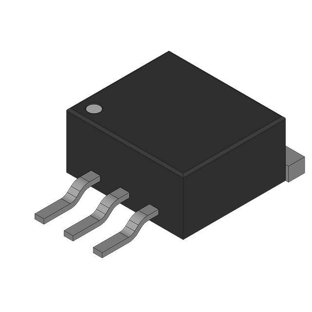
D2PAK 5
CASE 936A
ADJUSTABLE
Tab = Ground
Pin 1. N.C.
2. Vin
3. Ground
4. Vout
5. Adj
Typical Applications
•
•
•
•
D2PAK 3
CASE 936
FIXED
xx
y
A
WL
Y
WW
G
= 12 or 33
= P or V
= Assembly Location
= Wafer Lot
= Year
= Work Week
= Pb−Free
P565
MNxx
AYWWG
G
DFN6, 3x3.3
CASE 506AX
1
xx
= Voltage Rating
AJ = Adjustable
12 = 1.2 V 30 = 3.0V
15 = 1.5 V 33 = 3.3 V
28 = 2.8 V
AYW
565yy G
G
SOT−223
CASE 318E
1
yy
A
Y
W
G
= Voltage Rating
12 = 1.2 V
= Assembly Location
= Year
= Work Week
= Pb−Free Package
Tab = Vout
Pin 1. Ground
2. Vout
3. Vin
(Note: Microdot may be in either location)
ORDERING INFORMATION
See detailed ordering and shipping information in the package
dimensions section on page 11 of this data sheet.
© Semiconductor Components Industries, LLC, 2016
September, 2020 − Rev. 19
1
Publication Order Number:
NCP565/D
�NCP565, NCV565
Vin
Vin
Vout
Vout
Vin
Vin
NCP565
Vout
Vout
NCP565
GND
GND
Cout
Cin
C1
5.6 pF
ADJ
R1
Cout
Cin
R2
Figure 1. Typical Application Schematic,
Fixed Output
Figure 2. Typical Application Schematic,
Adjustable Output
PIN DESCRIPTION
D2PAK 5
D2PAK 3
Pin No.
Adj. Version
Pin No.
Fixed Version
Pin No.
Adj. Version
1
−
1, 2
1, 2, 5
−
N.C.
2
1
3
3
3
Vin
3, Tab
2, Tab
6
6
1
Ground
4
3
4
4
2, Tab
Vout
Regulated Output Voltage
5
−
5
−
−
Adj
This pin is to be connected to the sense
resistors on the output. The linear
regulator will attempt to maintain 0.9 V
between this pin and ground. Refer to
the Application Information section for
output voltage setting.
DFN6
SOT−223
Pin No.
Pin No.
Fixed Version Fixed Version
Vin
Symbol
Description
−
Positive Power Supply Input Voltage
Power Supply Ground
Vout Vin
Vout
Vref = 0.9 V
Vref = 0.9 V
Output
Stage
Voltage
Reference
Block
Current
Limit
Sense
Output
Stage
Voltage
Reference
Block
Current
Limit
Sense
ADJ
Thermal
Shutdown
Block
Thermal
Shutdown
Block
GND
GND
Figure 3. Block Diagram, Fixed Output
Figure 4. Block Diagram, Adjustable Output
www.onsemi.com
2
�NCP565, NCV565
ABSOLUTE MAXIMUM RATINGS
Symbol
Value
Unit
Input Voltage (Note 1)
Rating
Vin
18
V
Output Pin Voltage
Vout
−0.3 to Vin + 0.3
V
Adjust Pin Voltage
Vadj
−0.3 to Vin + 0.3
V
Stresses exceeding those listed in the Maximum Ratings table may damage the device. If any of these limits are exceeded, device functionality
should not be assumed, damage may occur and reliability may be affected.
NOTE:
This device series contains ESD protection and exceeds the following tests:
Human Body Model JESD 22−A114−B
Machine Model JESD 22−A115−A
THERMAL CHARACTERISTICS
Rating
Symbol
Value
Unit
Thermal Characteristics SOT−223 (Notes 1, 2)
Thermal Resistance, Junction−to−Ambient
Thermal Resistance, Junction−to−Pin
RqJA
RqJP
107
12
Thermal Characteristics DFN6 (Notes 1, 2)
Thermal Resistance, Junction−to−Ambient
Thermal Resistance, Junction−to−Pin
RqJA
RqJP
176
37
Thermal Characteristics D2PAK (5ld) (Notes 1, 2)
Thermal Resistance, Junction−to−Case
Thermal Resistance, Junction−to−Ambient
Thermal Resistance, Junction−to−Pin
RqJC
RqJA
RqJP
3
83
4
Symbol
Value
Unit
Operating Input Voltage (Note 1)
Vin
Vout + VDO,
2.5 (Note 3) to 9
V
Operating Junction Temperature Range
TJ
−40 to 150
°C
Operating Ambient Temperature Range
TA
−40 to 125
°C
Storage Temperature Range
Tstg
−55 to 150
°C
°C/W
°C/W
°C/W
OPERATING RANGES
Rating
1. Refer to Electrical Characteristics and Application Information for Safe Operating Area.
2. As measured using a copper heat spreading area of 50 mm2 for SOT−223 and DFN6, 100 mm2 for D2PAK, 1 oz copper thickness.
3. Minimum Vin = (Vout + VDO) or 2.5 V, whichever is higher.
www.onsemi.com
3
�NCP565, NCV565
ELECTRICAL CHARACTERISTICS (Vin = Vout + 1.6 V, Vout = 0.9 V, TA= 25°C, Cin = Cout = 150 mF, unless otherwise noted, Note 4.)
Characteristic
Symbol
Min
Typ
Max
Unit
Reference Voltage (10 mA < Iout < 1.5 A; Vout + 1.6 V < Vin < 9.0 V; TA = −10 to 105°C)
Vref
0.882
(−2%)
0.9
0.918
(+2%)
V
Reference Voltage (10 mA < Iout < 1.5 A; Vout + 1.6 V < Vin < 9.0 V; TA = −40 to 125°C)
Vref
0.873
(−3%)
0.9
0.927
(+3%)
V
ADJ Pin Current (Note 5)
IAdj
−
30
−
nA
Line Regulation (Iout = 10 mA) (Note 5)
Regline
−
0.03
−
%
Load Regulation (10 mA < Iout < 1.5 A) (Note 5)
Regload
−
0.03
−
%
ADJUSTABLE OUTPUT VERSION
Dropout Voltage (Iout = 1.5 A, Vout = 2.5 V) (Note 6)
Vdo
−
0.9
1.3
V
Current Limit
Ilim
1.6
3.3
−
A
Ripple Rejection (120 Hz; Iout = 1.5 A) (Note 5)
RR
−
85
−
dB
Ripple Rejection (1 kHz; Iout = 1.5 A) (Note 5)
Ground Current (Iout = 1.5 A)
Output Noise Voltage (f = 100 Hz to 100 kHz, Iout = 1.5 A) (Note 5)
Thermal Shutdown Protection (Note 5)
RR
−
75
−
dB
IGND
−
1.5
3.0
mA
Vn
−
28
−
mVrms
TSHD
−
160
−
_C
FIXED OUTPUT VOLTAGE (Vin = Vout + 1.6 V, TA = 25°C, Cin = Cout = 150 mF, unless otherwise noted, Note 4.)
Output Voltage (10 mA < Iout < 1.5 A; 2.8 V < Vin < 9.0 V; TA = −10 to 105°C)
1.2 V version
Vout
1.176
(−2%)
1.2
1.224
(+2%)
V
Output Voltage (10 mA < Iout < 1.5 A; 2.8 V < Vin < 9.0 V; TA = −40 to 125°C)
1.2 V version
Vout
1.164
(−3%)
1.2
1.236
(+3%)
V
Output Voltage (10 mA < Iout < 1.5 A; 3.1 V < Vin < 9.0 V; TA = −10 to 105°C)
1.5 V version
Vout
1.470
(−2%)
1.5
1.530
(+2%)
V
Output Voltage (10 mA < Iout < 1.5 A; 3.1 V < Vin < 9.0 V; TA = −40 to 125°C)
1.5 V version
Vout
1.455
(−3%)
1.5
1.545
(+3%)
V
Output Voltage (10 mA < Iout < 1.5 A; 4.4 V < Vin < 9.0 V; TA = −10 to 105°C)
2.8 V version
Vout
2.744
(−2%)
2.8
2.856
(+2%)
V
Output Voltage (10 mA < Iout < 1.5 A; 4.4 V < Vin < 9.0 V; TA = −40 to 125°C)
2.8 V version
Vout
2.716
(−3%)
2.8
2.884
(+3%)
V
Output Voltage (10 mA < Iout < 1.5 A; 4.6 V < Vin < 9.0 V; TA = −10 to 105°C)
3.0 V version
Vout
2.940
(−2%)
3.0
3.060
(+2%)
V
Output Voltage (10 mA < Iout < 1.5 A; 4.6 V < Vin < 9.0 V; TA = −40 to 125°C)
3.0 V version
Vout
2.910
(−3%)
3.0
3.090
(+3%)
V
Output Voltage (10 mA < Iout < 1.5 A; 4.9 V < Vin < 9.0 V; TA = −10 to 105°C)
3.3 V version
Vout
3.234
(−2%)
3.3
3.366
(+2%)
V
Output Voltage (10 mA < Iout < 1.5 A; 4.9 V < Vin < 9.0 V; TA = −40 to 125°C)
3.3 V version
Vout
3.201
(−3%)
3.3
3.399
(+3%)
V
Line Regulation (Iout = 10 mA) (Note 5)
Regline
−
0.03
−
%
Load Regulation (10 mA < Iout < 1.5 A) (Note 5)
Regload
−
0.03
−
%
Vdo
−
0.9
1.3
V
Current Limit
Ilim
1.6
3.3
−
A
Ripple Rejection (120 Hz; Iout = 1.5 A) (Note 5)
RR
−
85
−
dB
Ripple Rejection (1 kHz; Iout = 1.5 A) (Note 5)
RR
−
75
−
dB
IGND
−
1.5
3.0
mA
Vn
−
38
−
mVrms
TSHD
−
160
−
_C
Dropout Voltage (Iout = 1.5 A, Vout = 2.5 V) (Note 6)
Ground Current (Iout = 1.5 A)
Output Noise Voltage (f = 100 Hz to 100 kHz, Vout = 1.2 V, Iout = 1.5 A) (Note 5)
Thermal Shutdown Protection (Note 5)
4. Performance guaranteed over specified operating conditions by design, guard banded test limits, and/or characterization, production tested at
TJ = TA = 25_C. Low duty cycle pulse techniques are used during testing to maintain the junction temperature as close to ambient as possible.
5. Typical values are based on design and/or characterization.
6. Dropout voltage is a measurement of the minimum input/output differential at full load.
www.onsemi.com
4
�NCP565, NCV565
TYPICAL CHARACTERISTICS
3.302
Vref, REFERENCE VOLTAGE (V)
Vref, REFERENCE VOLTAGE (V)
0.9005
0.9000
0.8995
0.8990
0.8985
0.8980
Vin = 2.5 V
Vout(nom) = 0.9 V
0.8975
0.8970
−50
0
−25
25
50
75
100
125
3.300
3.298
3.296
3.294
3.292
Vin = 4.9 V
Vout(nom) = 3.3 V
3.290
3.288
−50
150
75
100
150
125
1.2
Vin − Vout, DROPOUT VOLTAGE (V)
ISC, SHORT CIRCUIT CURRENT LIMIT (A)
3.80
3.70
3.60
3.50
3.40
3.30
3.20
3.10
−25
0
25
50
75
100
125
1.0
0.6
Iout = 50 mA
0.4
0.2
0
−50
150
Iout = 1.5 A
0.8
TJ, JUNCTION TEMPERATURE (°C)
−25
0
25
50
75
100
125
150
TJ, JUNCTION TEMPERATURE (°C)
Figure 7. Short Circuit Current Limit
vs. Temperature
Figure 8. Dropout Voltage vs. Temperature
1.80
IGND, GROUND CURRENT (mA)
1.60
IGND, GROUND CURRENT (mA)
50
Figure 6. Output Voltage vs. Temperature
Figure 5. Output Voltage vs. Temperature
1.55
1.50
Iout = 1.5 A
1.45
1.40
1.35
1.30
−50
25
TJ, JUNCTION TEMPERATURE (°C)
TJ, JUNCTION TEMPERATURE (°C)
3.00
−50
0
−25
−25
25
75
125
0
50
100
TJ, JUNCTION TEMPERATURE (°C)
150
1.70
1.65
1.60
1.55
1.50
1.45
1.40
1.35
0
300
600
900
1200
1500
Iout, OUTPUT CURRENT (mA)
Figure 9. Ground Current vs. Temperature
Figure 10. Ground Current vs. Output Current
www.onsemi.com
5
�NCP565, NCV565
TYPICAL CHARACTERISTICS
100
1000
80
Unstable
70
100
60
ESR (W)
RIPPLE REJECTION (dB)
90
50
40
10
Iout = 1.5 A
30
20
0
10
100
1000
10000
1
100000 1000000
0
250
OUTPUT VOLTAGE
DEVIATION (mV)
10
0
−10
Vin = 4.59 V
Vout = 0.9 V
−30
−40
1.50
1.00
0.50
0
0
50
100
150
200
250
500
750
300
350
0
Vin = 4.59 V
Vout = 0.9 V
−20
−30
−40
1.50
1.00
0.50
0
400
0
0.5
1.0
1.5
OUTPUT VOLTAGE
DEVIATION (mV)
10
0
1.50
Iout, OUTPUT
CURRENT (A)
OUTPUT VOLTAGE
DEVIATION (mV)
Iout, OUTPUT
CURRENT (A)
Vin = 4.59 V
Vout = 0.9 V
1.00
0.50
0
50
100
150
200
2.5
3.0
3.5
4.0
Figure 14. Load Transient from 10 mA to 1.5 A
40
0
2.0
TIME (ms)
50
−50
1500
−10
Figure 13. Load Transient from 10 mA to 1.5 A
20
1250
10
TIME (nS)
30
1000
Figure 12. Output Capacitor ESR Stability vs.
Output Current
Iout, OUTPUT
CURRENT (A)
OUTPUT VOLTAGE
DEVIATION (mV)
Figure 11. Ripple Rejection vs. Frequency
−20
Cout = 10 mF
OUTPUT CURRENT (mA)
F, FREQUENCY (Hz)
Iout, OUTPUT
CURRENT (A)
Vout = 3.3 V
Stable
10
250
300
350
50
40
30
Vin = 4.59 V
Vout = 0.9 V
20
10
0
1.50
1.00
0.50
400
TIME (nS)
0
0
0.2
0.4
0.6
0.8
1.0
1.2
1.4
1.6
TIME (ms)
Figure 15. Load Transient from 1.5 A to 10 mA
Figure 16. Load Transient from 1.5 A to 10 mA
www.onsemi.com
6
�NCP565, NCV565
100
100
90
90
NOISE DENSITY (nVrms/ǰHz)
NOISE DENSITY (nVrms/ǰHz)
TYPICAL CHARACTERISTICS
80
70
60
Vin = 3.0 V
Vout = 0.9 V
Iout = 10 mA
50
40
30
20
10
0
Start 1.0 kHz
FREQUENCY (kHz)
80
70
Vin = 3.0 V
Vout = 0.9 V
Iout = 1.5 A
60
50
40
30
20
10
0
Start 1.0 kHz
Stop 100 kHz
Figure 17. Noise Density vs. Frequency
FREQUENCY (kHz)
Stop 100 kHz
Figure 18. Noise Density vs. Frequency
NOTE: Typical characteristics were measured with the same conditions as electrical characteristics.
APPLICATION INFORMATION
Adjustable Operation
The NCP565 low dropout linear regulator provides
adjustable voltages at currents up to 1.5 A. It features ultra
fast transient response and low dropout voltage. These
devices contain output current limiting, short circuit
protection and thermal shutdown protection.
The typical application circuit for the adjustable output
regulators is shown in Figure 2. The adjustable device
develops and maintains the nominal 0.9 V reference voltage
between Adj and ground pins. A resistor divider network R1
and R2 causes a fixed current to flow to ground. This current
creates a voltage across R1 that adds to the 0.9 V across R2
and sets the overall output voltage.
The output voltage is set according to the formula:
Input, Output Capacitor and Stability
An input bypass capacitor is recommended to improve
transient response or if the regulator is located more than a
few inches from the power source. This will reduce the
circuit’s sensitivity to the input line impedance at high
frequencies and significantly enhance the output transient
response. Different types and different sizes of input
capacitors can be chosen dependent on the quality of power
supply. A 150 mF OSCON 16SA150M type from Sanyo
should be adequate for most applications. The bypass
capacitor should be mounted with shortest possible lead or
track length directly across the regulator’s input terminals.
The output capacitor is required for stability. The NCP565
remains stable with ceramic, tantalum, and aluminum−
electrolytic capacitors with a minimum value of 1.0 mF with
ESR between 50 mW and 2.5 W. The NCP565 is optimized
for use with a 150 mF OSCON 16SA150M type in parallel
with a 10 mF OSCON 10SL10M type from Sanyo. The
10 mF capacitor is used for best AC stability while 150 mF
capacitor is used for achieving excellent output transient
response. The output capacitors should be placed as close as
possible to the output pin of the device. If not, the excellent
load transient response of NCP565 will be degraded.
Vout + Vref
) R2Ǔ * I
ǒR1 R2
Adj
R2
The adjust pin current, IAdj, is typically 30 nA and
normally much lower than the current flowing through R1
and R2, thus it generates a small output voltage error that can
usually be ignored.
Load Transient Measurement
Large load current changes are always presented in
microprocessor applications. Therefore good load transient
performance is required for the power stage. NCP565 has
the feature of ultra fast transient response. Its load transient
responses in Figures 13 through 16 are tested on evaluation
board shown in Figure 19. On the evaluation board, it
consists of NCP565 regulator circuit with decoupling and
filter capacitors and the pulse controlled current sink to
obtain load current transitions. The load current transitions
are measured by current probe. Because the signal from
current probe has some time delay, it causes
un−synchronization between the load current transition and
output voltage response, which is shown in Figures 13
through 16.
www.onsemi.com
7
�NCP565, NCV565
GEN
Vout
−VCC
Vin
Pulse
V
NCP565
RL
Evaluation Board
+
GND
+
GND
Scope Voltage Probe
Figure 19. Schematic for Transient Response Measurement
PCB Layout Considerations
several capacitors in parallel. This reduces the overall ESR
and reduces the instantaneous output voltage drop under
transient load conditions. The output capacitor network
should be as close as possible to the load for the best results.
The schematic of NCP565 typical application circuit, which
this PCB layout is base on, is shown in Figure 20. The output
voltage is set to 3.3 V for this demonstration board according
to the feedback resistors in the Table 1.
Good PCB layout plays an important role in achieving
good load transient performance. Because it is very sensitive
to its PCB layout, particular care has to be taken when
tackling Printed Circuit Board (PCB) layout. The figures
below give an example of a layout where parasitic elements
are minimized. For microprocessor applications it is
customary to use an output capacitor network consisting of
2
Vin
C1
150 m
C2
150 m
1
Vin
Vout
Vout
4
NCP565
Adj
NC
5
C4
10 m
GND
C3
150 m
3
C3
150 m
GND
GND
R2
R1
15.8 k
42.2 k
C6
5.6 p
Figure 20. Schematic of NCP565 Typical Application Circuit
www.onsemi.com
8
�NCP565, NCV565
Figure 21. Top Layer
Figure 22. Bottom Layer
NCP565
ON Semiconductor
www.onsemi.com
D1
VIN
R2
C2
VOUT
C3
C4
C1
R1C6
C5
GND
GND
July, 2003
Figure 23. Silkscreen Layer
www.onsemi.com
9
�NCP565, NCV565
Table 1. Bill of Materials for NCP565 Adj Demonstration Board
Item
Used #
Component
Designators
Suppliers
Part Number
1
4
Radial Lead Aluminum Capacitor
150 mF/16 V
C1, C2, C3, C5
Sanyo Oscon
16SA150M
2
1
Radial Lead Aluminum Capacitor
10 mF/10 V
C4
Sanyo Oscon
10SL10M
3
1
SMT Chip Resistor (0805) 15.8 K 1%
R2
Vishay
CRCW08051582F
4
1
SMT Chip Resistor (0805) 42.2 K 1%
R1
Vishay
CRCW08054222F
5
1
SMT Ceramic Capacitor (0603) 5.6 pF 10%
C6
Vishay
VJ0603A5R6KXAA
6
1
NCP565 Low Dropout Linear Regulator
U1
ON Semiconductor
NCP565D2TR4
Protection Diodes
Thermal Considerations
When large external capacitors are used with a linear
regulator it is sometimes necessary to add protection diodes.
If the input voltage of the regulator gets shorted, the output
capacitor will discharge into the output of the regulator. The
discharge current depends on the value of the capacitor, the
output voltage and the rate at which Vin drops. In the
NCP565 linear regulator, the discharge path is through a
large junction and protection diodes are not usually needed.
If the regulator is used with large values of output
capacitance and the input voltage is instantaneously shorted
to ground, damage can occur. In this case, a diode connected
as shown in Figure 24 is recommended.
This series contains an internal thermal limiting circuit
that is designed to protect the regulator in the event that the
maximum junction temperature is exceeded. This feature
provides protection from a catastrophic device failure due to
accidental overheating. It is not intended to be used as a
substitute for proper heat sinking. The maximum device
power dissipation can be calculated by:
PD +
TJ(max) * TA
RqJA
200
180
160
1N4002 (Optional)
Vin
C1
NCP565
GND
Vout
Vout
Adj
CAdj
R1
qJA (°C/W)
Vin
C2
140
DFN 1 oz Cu
DFN 2 oz Cu
SOT−223 1 oz Cu
120
SOT−223 2 oz Cu
D2PAK 1 oz Cu
100
D2PAK 2 oz Cu
80
R2
60
40
0
Figure 24. Protection Diode for Large
Output Capacitors
50 100 150
200 250 300 350 400 450 500
COPPER HEAT−SPREADER AREA (mm sq)
Figure 25. Thermal Resistance
www.onsemi.com
10
�NCP565, NCV565
ORDERING INFORMATION
Device
Nominal Output Voltage**
Package
D2PAK
NCP565D2TG
Shipping†
5
(Pb−Free)
50 Units / Tube
D2PAK 5
(Pb−Free)
800 / Tape & Reel
NCP565MNADJT2G
DFN6
(Pb−Free)
3000 / Tape & Reel
NCP565D2T12G
D2PAK 3
(Pb−Free)
50 Units / Tube
NCP565D2T12R4G
D2PAK 3
(Pb−Free)
800 / Tape & Reel
DFN6
(Pb−Free)
3000 / Tape & Reel
SOT−223
(Pb−Free)
4000 / Tape & Reel
Fixed (1.5 V)
DFN6
(Pb−Free)
3000 / Tape & Reel
Fixed (2.8 V)
DFN6
(Pb−Free)
3000 / Tape & Reel
Fixed (3.0 V)
DFN6
(Pb−Free)
3000 / Tape & Reel
D2PAK 3
(Pb−Free)
50 Units / Tube
D2PAK 3
(Pb−Free)
800 / Tape & Reel
DFN6
(Pb−Free)
3000 / Tape & Reel
D2PAK 5
(Pb−Free)
50 Units / Tube
NCP565D2TR4G
NCP565MN12T2G
Adj
Fixed (1.2 V)
NCP565ST12T3G
NCP565MN15T2G
NCP565MN28T2G
NCP565MN30T2G
NCP565D2T33G
NCP565D2T33R4G
Fixed (3.3 V)
NCP565MN33T2G
NCV565D2TG*
NCV565D2TR4G*
Adj
D2PAK
NCV565D2T12R4G*
NCV565ST12T3G*
Fixed (1.2 V)
800 / Tape & Reel
3
(Pb−Free)
800 / Tape & Reel
SOT−223
(Pb−Free)
4000 / Tape & Reel
†For information on tape and reel specifications, including part orientation and tape sizes, please refer to our Tape and Reel Packaging
Specifications Brochure, BRD8011/D.
*NCV Prefix for Automotive and Other Applications Requiring Unique Site and Control Change Requirements; AEC−Q100 Qualified and PPAP
Capable.
**For other fixed output versions, please contact the factory. The max Vout available for SOT−223 is 1.2 V.
www.onsemi.com
11
�MECHANICAL CASE OUTLINE
PACKAGE DIMENSIONS
SOT−223 (TO−261)
CASE 318E−04
ISSUE R
DATE 02 OCT 2018
SCALE 1:1
q
q
DOCUMENT NUMBER:
DESCRIPTION:
98ASB42680B
SOT−223 (TO−261)
Electronic versions are uncontrolled except when accessed directly from the Document Repository.
Printed versions are uncontrolled except when stamped “CONTROLLED COPY” in red.
PAGE 1 OF 2
ON Semiconductor and
are trademarks of Semiconductor Components Industries, LLC dba ON Semiconductor or its subsidiaries in the United States and/or other countries.
ON Semiconductor reserves the right to make changes without further notice to any products herein. ON Semiconductor makes no warranty, representation or guarantee regarding
the suitability of its products for any particular purpose, nor does ON Semiconductor assume any liability arising out of the application or use of any product or circuit, and specifically
disclaims any and all liability, including without limitation special, consequential or incidental damages. ON Semiconductor does not convey any license under its patent rights nor the
rights of others.
© Semiconductor Components Industries, LLC, 2018
www.onsemi.com
�SOT−223 (TO−261)
CASE 318E−04
ISSUE R
STYLE 1:
PIN 1.
2.
3.
4.
BASE
COLLECTOR
EMITTER
COLLECTOR
STYLE 2:
PIN 1.
2.
3.
4.
ANODE
CATHODE
NC
CATHODE
STYLE 6:
PIN 1.
2.
3.
4.
RETURN
INPUT
OUTPUT
INPUT
STYLE 7:
PIN 1.
2.
3.
4.
ANODE 1
CATHODE
ANODE 2
CATHODE
STYLE 11:
PIN 1. MT 1
2. MT 2
3. GATE
4. MT 2
STYLE 3:
PIN 1.
2.
3.
4.
GATE
DRAIN
SOURCE
DRAIN
STYLE 8:
STYLE 12:
PIN 1. INPUT
2. OUTPUT
3. NC
4. OUTPUT
CANCELLED
DATE 02 OCT 2018
STYLE 4:
PIN 1.
2.
3.
4.
SOURCE
DRAIN
GATE
DRAIN
STYLE 5:
PIN 1.
2.
3.
4.
STYLE 9:
PIN 1.
2.
3.
4.
INPUT
GROUND
LOGIC
GROUND
STYLE 10:
PIN 1. CATHODE
2. ANODE
3. GATE
4. ANODE
DRAIN
GATE
SOURCE
GATE
STYLE 13:
PIN 1. GATE
2. COLLECTOR
3. EMITTER
4. COLLECTOR
GENERIC
MARKING DIAGRAM*
AYW
XXXXXG
G
1
A
= Assembly Location
Y
= Year
W
= Work Week
XXXXX = Specific Device Code
G
= Pb−Free Package
(Note: Microdot may be in either location)
*This information is generic. Please refer to
device data sheet for actual part marking.
Pb−Free indicator, “G” or microdot “G”, may
or may not be present. Some products may
not follow the Generic Marking.
DOCUMENT NUMBER:
DESCRIPTION:
98ASB42680B
SOT−223 (TO−261)
Electronic versions are uncontrolled except when accessed directly from the Document Repository.
Printed versions are uncontrolled except when stamped “CONTROLLED COPY” in red.
PAGE 2 OF 2
ON Semiconductor and
are trademarks of Semiconductor Components Industries, LLC dba ON Semiconductor or its subsidiaries in the United States and/or other countries.
ON Semiconductor reserves the right to make changes without further notice to any products herein. ON Semiconductor makes no warranty, representation or guarantee regarding
the suitability of its products for any particular purpose, nor does ON Semiconductor assume any liability arising out of the application or use of any product or circuit, and specifically
disclaims any and all liability, including without limitation special, consequential or incidental damages. ON Semiconductor does not convey any license under its patent rights nor the
rights of others.
© Semiconductor Components Industries, LLC, 2018
www.onsemi.com
�MECHANICAL CASE OUTLINE
PACKAGE DIMENSIONS
DFN6 3.0x3.3, 0.95P
CASE 506AX
ISSUE A
DATE 22 SEP 2020
GENERIC
MARKING DIAGRAM*
XXXXX
XXXXX
AYWWG
G
DOCUMENT NUMBER:
DESCRIPTION:
XXXX = Specific Device Code
A
= Assembly Location
Y
= Year
WW = Work Week
G
= Pb−Free Package
(Note: Microdot may be in either location)
98AON21930D
DFN6 3.0X3.3, 0.95P
*This information is generic. Please refer to
device data sheet for actual part marking.
Pb−Free indicator, “G” or microdot “G”, may
or may not be present. Some products may
not follow the Generic Marking.
Electronic versions are uncontrolled except when accessed directly from the Document Repository.
Printed versions are uncontrolled except when stamped “CONTROLLED COPY” in red.
PAGE 1 OF 1
ON Semiconductor and
are trademarks of Semiconductor Components Industries, LLC dba ON Semiconductor or its subsidiaries in the United States and/or other countries.
ON Semiconductor reserves the right to make changes without further notice to any products herein. ON Semiconductor makes no warranty, representation or guarantee regarding
the suitability of its products for any particular purpose, nor does ON Semiconductor assume any liability arising out of the application or use of any product or circuit, and specifically
disclaims any and all liability, including without limitation special, consequential or incidental damages. ON Semiconductor does not convey any license under its patent rights nor the
rights of others.
© Semiconductor Components Industries, LLC, 2019
www.onsemi.com
�MECHANICAL CASE OUTLINE
PACKAGE DIMENSIONS
D2PAK
CASE 936−03
ISSUE E
DATE 29 SEP 2015
SCALE 1:1
T
C
A
K
B
J
C
ES
OPTIONAL
CHAMFER
DETAIL C
DETAIL C
3
F
G
SIDE VIEW
2X
TOP VIEW
D
0.010 (0.254)
N
DUAL GAUGE
CONSTRUCTION
P
BOTTOM VIEW
SIDE VIEW
SINGLE GAUGE
CONSTRUCTION
T
M
M
R
T
V
H
2
U
ED
OPTIONAL
CHAMFER
S
1
TERMINAL 4
T
SEATING
PLANE
L
BOTTOM VIEW
DETAIL C
OPTIONAL CONSTRUCTIONS
NOTES:
1. DIMENSIONING AND TOLERANCING PER ANSI
Y14.5M, 1982.
2. CONTROLLING DIMENSION: INCHES.
3. TAB CONTOUR OPTIONAL WITHIN DIMENSIONS
A AND K.
4. DIMENSIONS U AND V ESTABLISH A MINIMUM
MOUNTING SURFACE FOR TERMINAL 4.
5. DIMENSIONS A AND B DO NOT INCLUDE MOLD
FLASH OR GATE PROTRUSIONS. MOLD FLASH
AND GATE PROTRUSIONS NOT TO EXCEED
0.025 (0.635) MAXIMUM.
6. SINGLE GAUGE DESIGN WILL BE SHIPPED AF
TER FPCN EXPIRATION IN OCTOBER 2011.
DIM
A
B
C
D
ED
ES
F
G
H
J
K
L
M
N
P
R
S
U
V
INCHES
MIN
MAX
0.386
0.403
0.356
0.368
0.170
0.180
0.026
0.036
0.045
0.055
0.018
0.026
0.051 REF
0.100 BSC
0.539
0.579
0.125 MAX
0.050 REF
0.000
0.010
0.088
0.102
0.018
0.026
0.058
0.078
0_
8_
0.116 REF
0.200 MIN
0.250 MIN
MILLIMETERS
MIN
MAX
9.804 10.236
9.042
9.347
4.318
4.572
0.660
0.914
1.143
1.397
0.457
0.660
1.295 REF
2.540 BSC
13.691 14.707
3.175 MAX
1.270 REF
0.000
0.254
2.235
2.591
0.457
0.660
1.473
1.981
0_
8_
2.946 REF
5.080 MIN
6.350 MIN
GENERIC
MARKING DIAGRAM*
SOLDERING FOOTPRINT*
10.490
XXXXXXG
ALYWW
8.380
16.155
XXXXXX = Specific Device Code
A
= Assembly Location
L
= Wafer Lot
Y
= Year
WW
= Work Week
G
= Pb−Free Package
2X
3.504
2X
1.016
5.080
PITCH
DIMENSIONS: MILLIMETERS
*For additional information on our Pb−Free strategy and soldering
details, please download the ON Semiconductor Soldering and
Mounting Techniques Reference Manual, SOLDERRM/D.
DOCUMENT NUMBER:
DESCRIPTION:
98ASH01005A
D2PAK
*This information is generic. Please refer to
device data sheet for actual part marking.
Pb−Free indicator, “G” or microdot “ G”,
may or may not be present.
Electronic versions are uncontrolled except when accessed directly from the Document Repository.
Printed versions are uncontrolled except when stamped “CONTROLLED COPY” in red.
PAGE 1 OF 1
ON Semiconductor and
are trademarks of Semiconductor Components Industries, LLC dba ON Semiconductor or its subsidiaries in the United States and/or other countries.
ON Semiconductor reserves the right to make changes without further notice to any products herein. ON Semiconductor makes no warranty, representation or guarantee regarding
the suitability of its products for any particular purpose, nor does ON Semiconductor assume any liability arising out of the application or use of any product or circuit, and specifically
disclaims any and all liability, including without limitation special, consequential or incidental damages. ON Semiconductor does not convey any license under its patent rights nor the
rights of others.
© Semiconductor Components Industries, LLC, 2019
www.onsemi.com
�MECHANICAL CASE OUTLINE
PACKAGE DIMENSIONS
D2PAK 5−LEAD
CASE 936A−02
ISSUE E
DATE 28 JUL 2021
SCALE 1:1
GENERIC
MARKING DIAGRAM*
xx
xxxxxxxxx
AWLYWWG
xxxxxx
A
WL
Y
WW
G
= Device Code
= Assembly Location
= Wafer Lot
= Year
= Work Week
= Pb−Free Package
*This information is generic. Please refer to
device data sheet for actual part marking.
Pb−Free indicator, “G” or microdot “G”, may
or may not be present. Some products may
not follow the Generic Marking.
DOCUMENT NUMBER:
DESCRIPTION:
98ASH01006A
D2PAK 5−LEAD
Electronic versions are uncontrolled except when accessed directly from the Document Repository.
Printed versions are uncontrolled except when stamped “CONTROLLED COPY” in red.
PAGE 1 OF 1
ON Semiconductor and
are trademarks of Semiconductor Components Industries, LLC dba ON Semiconductor or its subsidiaries in the United States and/or other countries.
ON Semiconductor reserves the right to make changes without further notice to any products herein. ON Semiconductor makes no warranty, representation or guarantee regarding
the suitability of its products for any particular purpose, nor does ON Semiconductor assume any liability arising out of the application or use of any product or circuit, and specifically
disclaims any and all liability, including without limitation special, consequential or incidental damages. ON Semiconductor does not convey any license under its patent rights nor the
rights of others.
© Semiconductor Components Industries, LLC, 2019
www.onsemi.com
�onsemi,
, and other names, marks, and brands are registered and/or common law trademarks of Semiconductor Components Industries, LLC dba “onsemi” or its affiliates
and/or subsidiaries in the United States and/or other countries. onsemi owns the rights to a number of patents, trademarks, copyrights, trade secrets, and other intellectual property.
A listing of onsemi’s product/patent coverage may be accessed at www.onsemi.com/site/pdf/Patent−Marking.pdf. onsemi reserves the right to make changes at any time to any
products or information herein, without notice. The information herein is provided “as−is” and onsemi makes no warranty, representation or guarantee regarding the accuracy of the
information, product features, availability, functionality, or suitability of its products for any particular purpose, nor does onsemi assume any liability arising out of the application or use
of any product or circuit, and specifically disclaims any and all liability, including without limitation special, consequential or incidental damages. Buyer is responsible for its products
and applications using onsemi products, including compliance with all laws, regulations and safety requirements or standards, regardless of any support or applications information
provided by onsemi. “Typical” parameters which may be provided in onsemi data sheets and/or specifications can and do vary in different applications and actual performance may
vary over time. All operating parameters, including “Typicals” must be validated for each customer application by customer’s technical experts. onsemi does not convey any license
under any of its intellectual property rights nor the rights of others. onsemi products are not designed, intended, or authorized for use as a critical component in life support systems
or any FDA Class 3 medical devices or medical devices with a same or similar classification in a foreign jurisdiction or any devices intended for implantation in the human body. Should
Buyer purchase or use onsemi products for any such unintended or unauthorized application, Buyer shall indemnify and hold onsemi and its officers, employees, subsidiaries, affiliates,
and distributors harmless against all claims, costs, damages, and expenses, and reasonable attorney fees arising out of, directly or indirectly, any claim of personal injury or death
associated with such unintended or unauthorized use, even if such claim alleges that onsemi was negligent regarding the design or manufacture of the part. onsemi is an Equal
Opportunity/Affirmative Action Employer. This literature is subject to all applicable copyright laws and is not for resale in any manner.
PUBLICATION ORDERING INFORMATION
LITERATURE FULFILLMENT:
Email Requests to: orderlit@onsemi.com
onsemi Website: www.onsemi.com
◊
TECHNICAL SUPPORT
North American Technical Support:
Voice Mail: 1 800−282−9855 Toll Free USA/Canada
Phone: 011 421 33 790 2910
Europe, Middle East and Africa Technical Support:
Phone: 00421 33 790 2910
For additional information, please contact your local Sales Representative
�