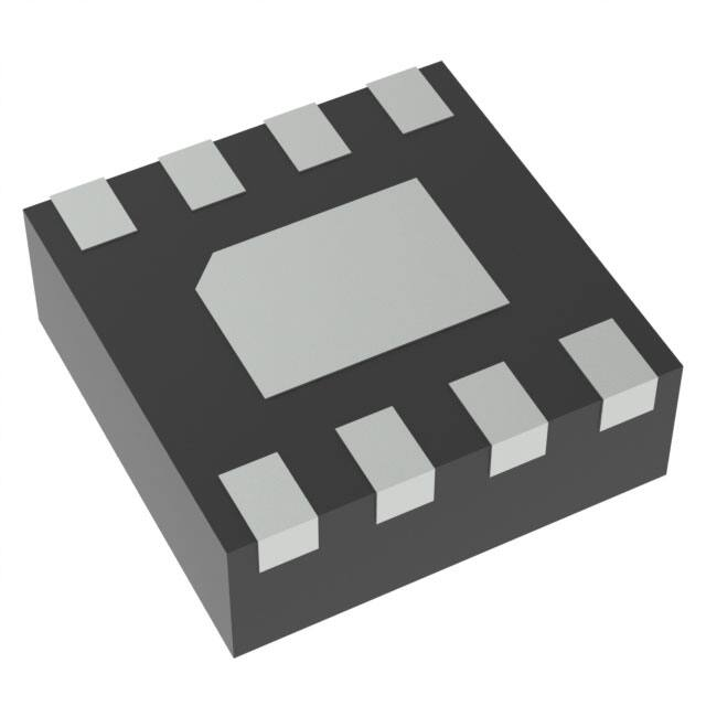
NCP5901B
MOSFET Driver, VR12
Compatible, Synchronous
Buck
The NCP5901B is a high performance dual MOSFET gate driver
optimized to drive the gates of both high−side and low−side power
MOSFETs in a synchronous buck converter. It can drive up to 3 nF
load with a 25 ns propagation delay and 20 ns transition time.
Adaptive anti−cross−conduction and power saving operation
circuit can provide a low switching loss and high efficiency solution
for notebook and desktop systems. Bidirectional EN pin can provide
a fault signal to controller when the gate driver fault detect under
OVP, UVLO occur. Also, an under−voltage lockout function
guarantees the outputs are low when supply voltage is low.
http://onsemi.com
8
1
1
SOIC−8 NB
D SUFFIX
CASE 751
DFN8
MN SUFFIX
CASE 506AA
Features
•
•
•
•
•
•
•
•
•
•
•
•
Faster Rise and Fall Times
Adaptive Anti−Cross−Conduction Circuit
Integrated Bootstrap Diode
Pre OV function
ZCD Detect
Floating Top Driver Accommodates Boost Voltages of up to 35 V
Output Disable Control Turns Off Both MOSFETs
Under−voltage Lockout
Power Saving Operation Under Light Load Conditions
Direct Interface to NCP6151 and Other Compatible PWM
Controllers
Thermally Enhanced Package
These are Pb−Free Devices
MARKING DIAGRAMS
8
5901B
ALYW
G
1
5901B
A
L
Y
W
G
= Specific Device Code
= Assembly Location
= Wafer Lot
= Year
= Work Week
= Pb−Free Package
1
Typical Applications
AZMG
G
AZ = Specific Device Code
M = Date Code
G
= Pb−Free Device
• Power Solutions for Desktop Systems
ORDERING INFORMATION
Device
Package
Shipping†
NCP5901BMNTBG
DFN8
3000 / Tape & Reel
(Pb−Free)
NCP5901BDR2G
SOIC−8 2500 / Tape & Reel
(Pb−Free)
†For information on tape and reel specifications,
including part orientation and tape sizes, please
refer to our Tape and Reel Packaging Specification
Brochure, BRD8011/D.
© Semiconductor Components Industries, LLC, 2013
June, 2013 − Rev. 2
1
Publication Order Number:
NCP5901B/D
�NCP5901B
BST
DRVH
1
PWM
SW
FLAG
9
EN
GND
VCC
DRVL
(Top View)
Figure 1. Pin Diagram
BST
VCC
DRVH
PWM
Logic
SW
Anti−Cross
Conduction
VCC
DRVL
EN
Fault
ZCD
Detection
UVLO
Pre−OV
Figure 2. Block Diagram
Table 1. Pin Descriptions
Pin No.
Symbol
Description
1
BST
Floating bootstrap supply pin for high side gate driver. Connect the bootstrap capacitor between this pin
and the SW pin.
2
PWM
Control input. The PWM signal has three distinctive states: Low = Low Side FET Enabled, Mid = Diode
Emulation Enabled, High = High Side FET Enabled.
3
EN
4
VCC
Power supply input. Connect a bypass capacitor (0.1 mF) from this pin to ground.
5
DRVL
Low side gate drive output. Connect to the gate of low side MOSFET.
6
GND
Bias and reference ground. All signals are referenced to this node (QFN Flag).
7
SW
8
DRVH
High side gate drive output. Connect to the gate of high side MOSFET.
9
FLAG
Thermal flag. There is no electrical connection to the IC. Connect to ground plane.
Logic input. A logic high to enable the part and a logic low to disable the part.
Switch node. Connect this pin to the source of the high side MOSFET and drain of the low side MOSFET.
http://onsemi.com
2
�NCP5901B
12V_POWER
TP1
R164
R1
1.02
R143
0.0
TP4
PWM
C4
0.027uF
EN
C2
4.7uF
TP5
+
CE9
390uF
TP6
GND
235nH
TP7
Q9
NTMFS4851N
VREG_SW1_LG
LG
VCCP
L
VREG_SW1_OUT
Q10
NTMFS4851N
R3
2.2
JP13_ETCH CSN11
PAD
TP8
C5
1uF
C3
4.7uF
0.0
VREG_SW1_HG
HG
VCC
C1
4.7uF
R142
PWM SW
DRON
TP2
0.0
NCP5901BTP3
BST
Q1
NTMFS4821N
C6
2700pF
JP14_ETCH CSP11
Figure 3. Application Circuit
Table 2. ABSOLUTE MAXIMUM RATINGS
Pin Symbol
Pin Name
VMAX
VMIN
VCC
Main Supply Voltage Input
15 V
−0.3 V
BST
Bootstrap Supply Voltage
35 V wrt/ GND
40 V ≤ 50 ns wrt/ GND
15 V wrt/ SW
−0.3 V wrt/SW
SW
Switching Node
(Bootstrap Supply Return)
35 V
40 V ≤ 50 ns
−5 V
−10 V (200 ns)
DRVH
High Side Driver Output
BST+0.3 V
−0.3 V wrt/SW
−2 V (
很抱歉,暂时无法提供与“NCP5901BMNTBG”相匹配的价格&库存,您可以联系我们找货
免费人工找货