DATA SHEET
www.onsemi.com
Linear Regulator Dual-Rail, Very
Low-Dropout,
Programmable Soft-Start
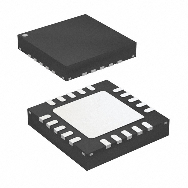
WLCSP10
CASE 567ZC
MARKING DIAGRAMS
3.0 A
1
NCP59744
The NCP59744 is dual−rail very low dropout voltage regulator that
is capable of providing an output current in excess of 3.0 A with a
dropout voltage of 75 mV typ. at full load current. The devices are
stable with ceramic and other low ESR output capacitors. This series
contains adjustable output voltage version with output voltage down
to 0.8 V. Internal protection features consist of built−in thermal
shutdown and output current limiting protection. User−programmable
Soft−Start and Power Good pins are available. The NCP59744 is
offered in DFN10 3x3, QFN20 5x5 and WLCSP10 packages.
Features
•
•
•
•
•
•
•
•
•
•
•
DFN10
CASE 485C
QFN20
CASE 485DB
Output Current in Excess of 3.0 A
0.25% Typical Accuracy Over Line and Load
VIN Range: 0.8 V to 5.5 V
VBIAS Range: 2.2 V to 5.5 V
Output Voltage Range: 0.8 V to 3.6 V
Dropout Voltage: 75 mV at 3 A
Programmable Soft Start
Open Drain Power Good Output
Excellent Transient Response
Current Limit and Thermal Shutdown Protection
These Devices are Pb−Free and are RoHS Compliant
1
NCP59744
AWLYYWWG
G
QFN20
NCP
59744
AYWG
G
DFN10
59744
ALYWW
WLCSP10
A
WL
YY, Y
WW, W
G
= Assembly Location
= Wafer Lot
= Year
= Work Week
= Pb-Free Package
(Note: Microdot may be in either location)
ORDERING INFORMATION
See detailed ordering, marking and shipping information on
page 13 of this data sheet.
Applications
•
•
•
•
Telecom and Industrial Equipment Point of Load Regulation
FPGA, DSP and Logic Power Supplies
Switching Power Supply Post Regulation
Applications with Specific Start−up Time or Sequencing
Requirements
NCP59744
Figure 1. Typical Application Schematic
© Semiconductor Components Industries, LLC, 2015
January, 2022 − Rev. 7
1
Publication Order Number:
NCP59744/D
�IN
NC
NC
NC
OUT
NCP59744
5
4
3
2
1
6
20
7
19
GND
8
9
18
17
10
16
11 12 13 14 15
EN
GND
NC
NC
SS
IN
IN
IN
PG
BIAS
QFN20−5y5−0.65P
(Top View)
OUT
OUT
OUT
NC
FB
IN
1
IN
PG
BIAS
EN
2
3
4
Thermal
Pad
10
OUT
9
OUT
FB
SS
GND
8
7
6
5
OUT
A1
A2
IN
OUT
B1
B2
IN
FB
C1
C2
PG
SS
D1
D2
BIAS
GND
E1
E2
EN
DFN10−3y3−0.5P
(Top View)
Figure 2. Pin Connections
Figure 3. Simplified Schematic Block Diagram
www.onsemi.com
2
WLCSP10
(Top View)
�NCP59744
Table 1. PIN FUNCTION DESCRIPTION
Name
DFN10
QFN20
WLCSP10
Description
IN
1, 2
5−8
A2, B2
EN
5
11
E2
Enable pin. Driving this pin high enables the regulator. Driving this pin low
puts the regulator into shutdown mode. This pin must not be left floating.
SS
7
15
D1
Soft−Start pin. A capacitor connected on this pin to ground sets the start−up
time. If this pin is left floating, the regulator output soft−start ramp time is
typically 200 ms.
BIAS
4
10
D2
Bias input voltage for error amplifier, reference, and internal control circuits.
PG
3
9
C2
Power−Good (PG) is an open−drain, active−high output that indicates the
status of VOUT. When VOUT exceeds the PG trip threshold, the PG pin goes
into a high−impedance state. When VOUT is below this threshold the pin is
driven to a low−impedance state. A pull−up resistor from 10 kW to 1 MW
should be connected from this pin to a supply up to 5.5 V. The supply can be
higher than the input voltage. Alternatively, the PG pin can be left floating if
output monitoring is not necessary.
FB
8
16
C1
This pin is the feedback connection to the center tap of an external resistor
divider network that sets the output voltage. This pin must not be left floating.
OUT
9, 10
1, 18−20
A1, B1
NC
N/A
2−4, 13, 14, 17
N/A
No connection. This pin can be left floating or connected to GND to allow
better thermal contact to the top−side plane.
GND
6
12
E1
Ground
PAD/TAB
Unregulated input to the device.
Regulated output voltage. It is recommended that the output capacitor
≥ 2.2 mF.
Should be soldered to the ground plane for increased thermal performance
Table 2. ABSOLUTE MAXIMUM RATINGS
Symbol
Value
Unit
Input Voltage Range
Parameter
VIN
−0.3 to +6
V
Input Voltage Range
VBIAS
−0.3 to +6
V
Enable Voltage Range
VEN
−0.3 to +6
V
Power−Good Voltage Range
VPG
−0.3 to +6
V
PG Sink Current
IPG
0 to +1.5
mA
SS Pin Voltage Range
VSS
−0.3 to +6
V
Feedback Pin Voltage Range
VFB
−0.3 to +6
V
Output Voltage Range
VOUT
−0.3 to (VIN + 0.3) ≤ 6
V
Maximum Output Current
IOUT
Internally Limited
PD
See Thermal Characteristics Table and Formula
TJMAX
+150
°C
Output Short Circuit Duration
Continuous Total Power Dissipation
Maximum Junction Temperature
Storage Junction Temperature Range
Indefinite
TSTG
−55 to +150
°C
ESD Capability, Human Body Model (Note 2)
ESDHBM
2000
V
ESD Capability, Machine Model (Note 2)
ESDMM
200
V
Stresses exceeding those listed in the Maximum Ratings table may damage the device. If any of these limits are exceeded, device functionality
should not be assumed, damage may occur and reliability may be affected.
1. Refer to ELECTRICAL CHARACTERISTICS and APPLICATION INFORMATION for Safe Operating Area.
2. This device series incorporates ESD protection and is tested by the following methods:
ESD Human Body Model tested per EIA/JESD22−A114
ESD Machine Model tested per EIA/JESD22−A115
Latch−up Current Maximum Rating tested per JEDEC standard: JESD78.
www.onsemi.com
3
�NCP59744
Table 3. THERMAL CHARACTERISTICS
Rating
Symbol
Value
Unit
Thermal Resistance, Junction−to−Ambient (Note 5)
RqJA
41.5
°C/W
Thermal Resistance, Junction−to−Case (bottom) (Note 7)
RqJC
6.6
°C/W
Thermal Resistance, Junction−to−Ambient (Note 5)
RqJA
35.4
°C/W
Thermal Resistance, Junction−to−Board (Note 6)
RqJB
14.7
°C/W
Thermal Resistance, Junction−to−Case (bottom) (Note 7)
RqJC
3.9
°C/W
Thermal Resistance, Junction−to−Ambient (Note 5)
RqJA
72
°C/W
Thermal Characterization Parameter, Junction−to−Case (top)
YJT
0.9
°C/W
Thermal Characteristics, DFN10, 3x3, 0.5P package
Thermal Characteristics, QFN20, 5x5, 0.65P package
Thermal Characteristics, WLCSP10 package
3. Refer to ELECTRICAL CHARACTERISTICS and APPLICATION INFORMATION for Safe Operating Area.
4. Thermal data are derived by thermal simulations based on methodology specified in the JEDEC JESD51 series standards. The following
assumptions are used in the simulations:
− These data were generated with only a single device at the center of a high−K (2s2p) board with 3 in x 3 in copper area which follows the
JEDEC51.7 guidelines. Top and Bottom layer 2 oz. copper, inner planes 1 oz. copper.
− DFN10: The exposed pad is connected to the PCB ground inner layer through a 3x2 thermal via array. Vias are 0.3 mm diameter, plated.
Each of top and bottom copper layers are assumed to have thermal conductivity representing 20% copper coverage.
− QFN20: The exposed pad is connected to the PCB ground inner layer through a 4x4 thermal via array. Vias are 0.3 mm diameter, plated.
Each of top and bottom copper layers has a dedicated pattern for 20% copper coverage.
5. The junction−to−ambient thermal resistance under natural convection is obtained in a simulation on a high−K board, following the JEDEC51.7
guidelines with assumptions as above, in an environment described in JESD51−2a.
6. The junction−to−board thermal resistance is simulated in an environment with a ring cold plate fixture to control the PCB temperature, as
described in JESD51−8.
7. The junction−to−case (bottom) thermal resistance is obtained by simulating a cold plate test on the IC exposed pad. Test description can
be found in the ANSI SEMI standard G30−88.
Table 4. RECOMMENDED OPERATING CONDITIONS (Note 8)
Rating
Symbol
Min
Max
Unit
Input Voltage
VIN
VOUT + VDO
5.5
V
Bias Voltage
VBIAS
2.2
5.5
V
TJ
−40
125
°C
Junction Temperature
Functional operation above the stresses listed in the Recommended Operating Ranges is not implied. Extended exposure to stresses beyond
the Recommended Operating Ranges limits may affect device reliability.
8. Refer to ELECTRICAL CHARACTERISTICS and APPLICATION INFORMATION for Safe Operating Area.
www.onsemi.com
4
�NCP59744
Table 5. ELECTRICAL CHARACTERISTICS − NCP59744FCTCADJT2G − WLCSP10
(At VEN = 1.1 V, VIN = VOUT + 0.3 V, CBIAS = CIN = 0.1 mF, COUT = 10 mF, IOUT = 50 mA, VBIAS = 5.0 V, TJ = −40°C to +125°C, unless
otherwise noted. Typical values are at TJ = +25°C.)
Symbol
VIN
Parameter
Test Conditions
Input voltage range
Min
Typ
VOUT +VDO
VBIAS
Bias pin voltage range
UVLO
Undervoltage Lock−out
VBIAS Rising Hysteresis
VREF
Internal reference (Adj.)
VOUT
Output voltage range
Unit
5.5
V
5.5
V
1.2
−
1.6
0.4
1.9
−
V
TJ = +25°C
0.796
0.8
0.804
V
VIN = 5 V, IOUT = 1.5 A, VBIAS = 5 V
VREF
Accuracy (Note 9)
2.97 V ≤ VBIAS ≤ 5.25 V, VOUT +
1.62 V ≤ VBIAS
50 mA ≤ IOUT ≤ 3.0 A
−1.0
VOUT/VIN
Line regulation
VOUT(NOM) + 0.3 ≤ VIN ≤ 5.5 V
0.0006
%/V
VOUT/IOUT
Load regulation
0 mA ≤ IOUT ≤ 50 mA
0.005
%/mA
50 mA ≤ IOUT ≤ 3.0 A
0.01
VDO
ICL
2.2
Max
VIN dropout voltage (Note 10)
IOUT = 3.0 A,
VBIAS – VOUT(NOM) ≥ 1.62 V
VBIAS dropout voltage (Note 10)
IOUT = 3.0 A, VIN = VBIAS
1.13
1.5
V
4.6
7
A
1.3
2
mA
1
15
mA
95
250
nA
VOUT = 80% x VOUT(NOM)
0 mA ≤ IOUT ≤ 3.0 A
ISHDN
Shutdown supply current
VEN ≤ 0.4 V
Feedback pin current
0 mA ≤ IOUT ≤ 3.0 A
Power−supply rejection
(VIN to VOUT)
1 kHz, IOUT = 1.5 A,
VIN = 1.8 V, VOUT = 1.5 V
72
1 MHz, IOUT = 1.5 A,
VIN = 1.8 V, VOUT = 1.5 V
50
1 kHz, IOUT = 1.5 A,
VIN = 1.8 V, VOUT = 1.5 V
80
1 MHz, IOUT = 1.5 A,
VIN = 1.8 V, VOUT = 1.5 V
48
Power−supply rejection
(VBIAS to VOUT)
Noise
Output noise voltage
100 Hz to 100 kHz, lOUT = 3 A
Css = 1.0 nF
VTRAN
%VOUT droop during load
transient
tSTRT
ISS
%/A
mV
Bias pin current
−250
%
140
Current limit
IFB
V
+1.0
75
IBIAS
PSRR
3.8
±0.25
3.6
dB
dB
18 x VOUT
mVrms
IOUT = 50 mA to 3.0 A at 1 A/ms,
COUT = 10 mF, VOUT = 3.3 V
±1.5
%VOUT
Minimum startup time
IOUT = 1.5 A, CSS = open
200
ms
Soft−start charging current
VSS = 0.4 V
0.45
mA
VEN, HI
Enable input high level
1.1
5.5
V
VEN, LO
Enable input low level
0
0.4
V
VEN,HYS
Enable pin hysteresis
100
mV
VEN,DG
Enable pin deglitch time
20
ms
IEN
Enable pin current
VEN = 5 V
VIT
PG trip threshold
VOUT decreasing
VHYS
PG trip hysteresis
86.5
0.3
1
mA
90
93.5
%VOUT
3
VPG, LO
PG output low voltage
IPG = 1 mA (sinking), VOUT < VIT
IPG, LKG
PG leakage current
VPG = 5.25 V, VOUT > VIT
0.03
Thermal shutdown temperature
Shutdown, temperature increasing
Reset, temperature decreasing
+165
+140
TSD
%VOUT
0.3
V
1
mA
°C
Product parametric performance is indicated in the Electrical Characteristics for the listed test conditions, unless otherwise noted. Product
performance may not be indicated by the Electrical Characteristics if operated under different conditions.
9. Adjustable devices tested at 0.8 V; external resistor tolerance is not taken into account.
10. Dropout is defined as the voltage from the input to VOUT when VOUT is 2% below nominal.
www.onsemi.com
5
�NCP59744
Table 6. ELECTRICAL CHARACTERISTICS − NCP59744MN1ADJTBG − DFN10
(At VEN = 1.1 V, VIN = VOUT + 0.3 V, CBIAS = CIN = 0.1 mF, COUT = 10 mF, IOUT = 50 mA, VBIAS = 5.0 V, TJ = −40°C to +125°C, unless
otherwise noted. Typical values are at TJ = +25°C.)
Symbol
VIN
Parameter
Test Conditions
Input voltage range
Min
Typ
VOUT +VDO
VBIAS
Bias pin voltage range
UVLO
Undervoltage Lock−out
VBIAS Rising Hysteresis
VREF
Internal reference (Adj.)
VOUT
Output voltage range
Unit
5.5
V
5.5
V
1.2
−
1.6
0.4
1.9
−
V
TJ = +25°C
0.796
0.8
0.804
V
VIN = 5 V, IOUT = 1.5 A, VBIAS = 5 V
VREF
Accuracy (Note 11)
2.97 V ≤ VBIAS ≤ 5.25 V, VOUT +
1.62 V ≤ VBIAS
50 mA ≤ IOUT ≤ 3.0 A
−1.0
VOUT/VIN
Line regulation
VOUT(NOM) + 0.3 ≤ VIN ≤ 5.5 V
0.0006
%/V
VOUT/IOUT
Load regulation
0 mA ≤ IOUT ≤ 50 mA
0.005
%/mA
50 mA ≤ IOUT ≤ 3.0 A
0.01
VDO
ICL
2.2
Max
VIN dropout voltage (Note 12)
IOUT = 3.0 A,
VBIAS – VOUT(NOM) ≥ 1.62 V
VBIAS dropout voltage (Note 12)
IOUT = 3.0 A, VIN = VBIAS
1.13
1.5
V
4.6
7
A
1.3
2
mA
1
15
mA
95
250
nA
VOUT = 80% x VOUT(NOM)
0 mA ≤ IOUT ≤ 3.0 A
ISHDN
Shutdown supply current
VEN ≤ 0.4 V
Feedback pin current
0 mA ≤ IOUT ≤ 3.0 A
Power−supply rejection
(VIN to VOUT)
1 kHz, IOUT = 1.5 A,
VIN = 1.8 V, VOUT = 1.5 V
72
1 MHz, IOUT = 1.5 A,
VIN = 1.8 V, VOUT = 1.5 V
50
1 kHz, IOUT = 1.5 A,
VIN = 1.8 V, VOUT = 1.5 V
80
1 MHz, IOUT = 1.5 A,
VIN = 1.8 V, VOUT = 1.5 V
48
Power−supply rejection
(VBIAS to VOUT)
Noise
Output noise voltage
100 Hz to 100 kHz, lOUT = 3 A
Css = 1.0 nF
VTRAN
%VOUT droop during load
transient
tSTRT
ISS
%/A
mV
Bias pin current
−250
%
160
Current limit
IFB
V
+1.0
95
IBIAS
PSRR
3.8
±0.25
3.6
dB
dB
18 x VOUT
mVrms
IOUT = 50 mA to 3.0 A at 1 A/ms,
COUT = 10 mF, VOUT = 3.3 V
±1.5
%VOUT
Minimum startup time
IOUT = 1.5 A, CSS = open
200
ms
Soft−start charging current
VSS = 0.4 V
0.45
mA
VEN, HI
Enable input high level
1.1
5.5
V
VEN, LO
Enable input low level
0
0.4
V
VEN,HYS
Enable pin hysteresis
100
mV
VEN,DG
Enable pin deglitch time
20
ms
IEN
Enable pin current
VEN = 5 V
VIT
PG trip threshold
VOUT decreasing
VHYS
PG trip hysteresis
86.5
0.3
1
mA
90
93.5
%VOUT
3
VPG, LO
PG output low voltage
IPG = 1 mA (sinking), VOUT < VIT
IPG, LKG
PG leakage current
VPG = 5.25 V, VOUT > VIT
0.03
Thermal shutdown temperature
Shutdown, temperature increasing
Reset, temperature decreasing
+165
+140
TSD
%VOUT
0.3
V
1
mA
°C
Product parametric performance is indicated in the Electrical Characteristics for the listed test conditions, unless otherwise noted. Product
performance may not be indicated by the Electrical Characteristics if operated under different conditions.
11. Adjustable devices tested at 0.8 V; external resistor tolerance is not taken into account.
12. Dropout is defined as the voltage from the input to VOUT when VOUT is 2% below nominal.
www.onsemi.com
6
�NCP59744
Table 7. ELECTRICAL CHARACTERISTICS − NCP59744MN2ADJTBG − QFN20
(At VEN = 1.1 V, VIN = VOUT + 0.3 V, CBIAS = CIN = 0.1 mF, COUT = 10 mF, IOUT = 50 mA, VBIAS = 5.0 V, TJ = −40°C to +125°C, unless
otherwise noted. Typical values are at TJ = +25°C.)
Symbol
VIN
Parameter
Test Conditions
Input voltage range
Min
Typ
VOUT +VDO
VBIAS
Bias pin voltage range
UVLO
Undervoltage Lock−out
VBIAS Rising Hysteresis
VREF
Internal reference (Adj.)
VOUT
Output voltage range
Unit
5.5
V
5.5
V
1.2
−
1.6
0.4
1.9
−
V
TJ = +25°C
0.796
0.8
0.804
V
VIN = 5 V, IOUT = 1.5 A, VBIAS = 5 V
VREF
Accuracy (Note 13)
2.97 V ≤ VBIAS ≤ 5.25 V, VOUT +
1.62 V ≤ VBIAS
50 mA ≤ IOUT ≤ 3.0 A
−1.0
VOUT/VIN
Line regulation
VOUT(NOM) + 0.3 ≤ VIN ≤ 5.5 V
0.0006
%/V
VOUT/IOUT
Load regulation
0 mA ≤ IOUT ≤ 50 mA
0.005
%/mA
50 mA ≤ IOUT ≤ 3.0 A
0.01
VIN dropout voltage (Note 14)
IOUT = 3.0 A,
VBIAS – VOUT(NOM) ≥ 1.62 V
115
195
mV
VBIAS dropout voltage (Note 14)
IOUT = 3.0 A, VIN = VBIAS
1.13
1.5
V
4.6
6
A
1.3
2
mA
1
10
mA
95
250
nA
VDO
ICL
2.2
Max
Current limit
VOUT = 80% x VOUT(NOM)
IBIAS
Bias pin current
0 mA ≤ IOUT ≤ 3.0 A
ISHDN
Shutdown supply current
VEN ≤ 0.4 V
Feedback pin current
0 mA ≤ IOUT ≤ 3.0 A
Power−supply rejection
(VIN to VOUT)
1 kHz, IOUT = 1.5 A,
VIN = 1.8 V, VOUT = 1.5 V
72
1 MHz, IOUT = 1.5 A,
VIN = 1.8 V, VOUT = 1.5 V
50
1 kHz, IOUT = 1.5 A,
VIN = 1.8 V, VOUT = 1.5 V
80
1 MHz, IOUT = 1.5 A,
VIN = 1.8 V, VOUT = 1.5 V
48
IFB
PSRR
Power−supply rejection
(VBIAS to VOUT)
Noise
Output noise voltage
100 Hz to 100 kHz, lOUT = 3 A
Css = 1.0 nF
VTRAN
%VOUT droop during load
transient
tSTRT
ISS
3.8
±0.25
−250
3.6
V
+1.0
%
%/A
dB
dB
18 x VOUT
mVrms
IOUT = 50 mA to 3.0 A at 1 A/ms,
COUT = 10 mF, VOUT = 3.3 V
±1.5
%VOUT
Minimum startup time
IOUT = 1.5 A, CSS = open
200
ms
Soft−start charging current
VSS = 0.4 V
0.45
mA
VEN, HI
Enable input high level
1.1
5.5
V
VEN, LO
Enable input low level
0
0.4
V
VEN,HYS
Enable pin hysteresis
100
mV
VEN,DG
Enable pin deglitch time
20
ms
IEN
Enable pin current
VEN = 5 V
VIT
PG trip threshold
VOUT decreasing
VHYS
PG trip hysteresis
86.5
0.3
1
mA
90
93.5
%VOUT
3
VPG, LO
PG output low voltage
IPG = 1 mA (sinking), VOUT < VIT
IPG, LKG
PG leakage current
VPG = 5.25 V, VOUT > VIT
0.03
Thermal shutdown temperature
Shutdown, temperature increasing
Reset, temperature decreasing
+165
+140
TSD
%VOUT
0.3
V
1
mA
°C
Product parametric performance is indicated in the Electrical Characteristics for the listed test conditions, unless otherwise noted. Product
performance may not be indicated by the Electrical Characteristics if operated under different conditions.
13. Adjustable devices tested at 0.8 V; external resistor tolerance is not taken into account.
14. Dropout is defined as the voltage from the input to VOUT when VOUT is 2% below nominal.
www.onsemi.com
7
�NCP59744
TYPICAL CHARACTERISTICS
0.20
0.5
0.15
0.4
0.10
−40°C
+125°C
0.05
0
CHANGE IN VOUT (%)
CHANGE IN VOUT (%)
At TJ = +25°C, VOUT = 1.5 V, VIN = VOUT(TYP) + 0.3 V, VBIAS = 3.3 V, IOUT = 50 mA, VEN = VIN,
CIN = 1 mF, CBIAS = 1 mF, CSS = 0.01 mF, and COUT = 10 mF, unless otherwise noted.
+25°C
−0.05
−0.10
−0.15
0.5
1.0
1.5
2.0
2.5
3.0
3.5
4.0
5.0
4.5
0
−0.1
−0.3
1.5
2.0
2.5
3.0
3.5
Figure 4. VIN Line Regulation
Figure 5. VBIAS Line Regulation
0.3
0.2
CHANGE IN VOUT (%)
0.4
+125°C
0.1
+25°C
0
−0.1
−0.2
−0.3
−40°C
10
20
30
40
50
+125°C
0.1
+25°C
0
−0.1
−0.2
−0.3
−40°C
0
0.5
1.0
1.5
2.0
2.5
IOUT, OUTPUT CURRENT (mA)
IOUT, OUTPUT CURRENT (A)
Figure 6. Load Regulation
Figure 7. Load Regulation
+125°C
120
100
+25°C
80
60
−40°C
40
20
1.0
1.5
2.0
3.0
2.5
3.0
500
450
IOUT = 3 A
400
350
300
250
200
+25°C
150
+125°C
100
50
0
−40°C
0.5
1.0
1.5
2.0
2.5
3.0
3.5
4.0
IOUT, OUTPUT CURRENT (A)
VBIAS − VOUT (V)
Figure 8. VIN Dropout Voltage vs. IOUT and
Temperature TJ
Figure 9. VIN Dropout Voltage vs. (VBIAS −
VOUT) and Temperature TJ
www.onsemi.com
8
4.0
0.2
−0.4
−0.5
140
0.5
1.0
VBIAS − VOUT (V)
0.3
0
0.5
VIN − VOUT (V)
0.4
0
+25°C
−0.2
0.5
0
+125°C
−40°C
0.1
0.5
−0.4
−0.5
VDO (VIN − VOUT) DROPOUT VOLTAGE (mV)
0
0.2
−0.4
−0.5
VDO (VIN − VOUT) DROPOUT VOLTAGE (mV)
CHANGE IN VOUT (%)
−0.20
0.3
4.5
�NCP59744
TYPICAL CHARACTERISTICS
VDO (VBIAS − VOUT) DROPOUT VOLTAGE (mV)
VDO (VIN − VOUT) DROPOUT VOLTAGE (mV)
At TJ = +25°C, VOUT = 1.5 V, VIN = VOUT(TYP) + 0.3 V, VBIAS = 3.3 V, IOUT = 50 mA, VEN = VIN,
CIN = 1 mF, CBIAS = 1 mF, CSS = 0.01 mF, and COUT = 10 mF, unless otherwise noted.
1400
200
180
1300
IOUT = 1.5 A
160
1200
140
120
+25°C
1000
100
80
+125°C
60
+25°C
40
−40°C
20
0
−40°C
1100
0.5
1.0
1.5
2.0
2.5
3.0
3.5
4.0
4.5
VBIAS − VOUT (V)
+125°C
900
800
700
600
0
2000
1800
1800
−40°C
1000
800
1200
−40°C
800
600
400
400
200
200
0
0
0.5
1.5
1.0
2.0
2.5
3.0
2.0
2.5
3.0
3.5
4.0
4.5
5.0
IOUT, OUTPUT CURRENT (A)
VBIAS (V)
Figure 12. BIAS Pin Current vs. IOUT and
Temperature TJ
Figure 13. BIAS Pin Current vs. VBIAS and
Temperature TJ
5.5
1.0
VPG,LO, L−LEVEL PG VOLTAGE (V)
0.500
0.475
0.450
ISS (mA)
3.0
+125°C
1000
600
0
2.5
+25°C
1400
IBIAS (mA)
1200
IBIAS (mA)
1600
+25°C
+125°C
2.0
Figure 11. VBIAS Dropout Voltage vs. IOUT and
Temperature TJ
2000
1400
1.5
1.0
IOUT, OUTPUT CURRENT (A)
Figure 10. VIN Dropout Voltage vs. (VBIAS −
VOUT) and Temperature TJ
1600
0.5
0.425
0.400
0.375
0.350
0.325
0.300
−50
−25
0
25
50
75
100
125
0.9
0.8
0.7
0.6
0.5
0.4
0.3
0.2
0.1
0
0
2
4
6
8
10
TJ, JUNCTION TEMPERATURE (°C)
IPG, PG PIN CURRENT (mA)
Figure 14. Soft Start Charging Current ISS vs.
Temperature TJ
Figure 15. L−level PG Voltage vs. Current
www.onsemi.com
9
12
�NCP59744
TYPICAL CHARACTERISTICS
At TJ = +25°C, VOUT = 1.5 V, VIN = VOUT(TYP) + 0.3 V, VBIAS = 3.3 V, IOUT = 50 mA, VEN = VIN,
CIN = 1 mF, CBIAS = 1 mF, CSS = 0.01 mF, and COUT = 10 mF, unless otherwise noted.
ICL, CURRENT LIMIT (A)
6.0
+25°C
−40°C
5.0
+125°C
4.0
3.0
2.0
1.0
0
0
0.5
1.0
1.5
2.0
2.5
3.0
3.5
4.0
4.5
5.0
Figure 16. Current Limit vs. (VBIAS − VOUT)
Figure 17. Start by Enable at CSS = 0
Figure 18. Start by Enable at CSS = 1 nF
Figure 19. Start by Enable at CSS = 10 nF
700
VIN = 1.3 V
VBIAS = 5 V
VOUTNOM = 0.8 V
ILOAD = 1500 mA
CBIAS = 1 mF
CIN = COUT = 10 mF
600
500
NOISE SPECTRAL DENSITY (nV/√Hz)
NOISE SPECTRAL DENSITY (nV/√Hz)
VBIAS − VOUT (V)
Resistive load
400
300
Css=0
200
100
0
Css=1nF
Css=10nF
10
100
1,000
10,000
100,000
106
1,200
VIN = 2.0 V
VBIAS = 5 V
VOUTNOM = 1.5 V
ILOAD = 1500 mA
CBIAS = 1 mF
CIN = COUT = 10 mF
1,000
800
Resistive load
600
Css=0
400
Css=1nF
200
0
Css=10nF
10
100
1,000
10,000
100,000
FREQUENCY (Hz)
FREQUENCY (Hz)
Figure 20. Output Voltage Noise Spectral
Density at VOUT = 0.8 V
Figure 21. Output Voltage Noise Spectral
Density at VOUT = 1.5 V
www.onsemi.com
10
106
�NCP59744
TYPICAL CHARACTERISTICS
2,400
90
VIN = 3.5 V
VBIAS = 5 V
VOUTNOM = 3.0 V
ILOAD = 1500 mA
CBIAS = 1 mF
CIN = COUT = 10 mF
2,000
1,600
80
70
Resistive load
PSRR (dB)
NOISE SPECTRAL DENSITY (nV/√Hz)
At TJ = +25°C, VOUT = 1.5 V, VIN = VOUT(TYP) + 0.3 V, VBIAS = 3.3 V, IOUT = 50 mA, VEN = VIN,
CIN = 1 mF, CBIAS = 1 mF, CSS = 0.01 mF, and COUT = 10 mF, unless otherwise noted.
1,200
Css=0
800
Css=1nF
400
0
10
50
40
30
20
Css=10nF
100
60
10
1,000
10,000
100,000
106
0
10
FREQUENCY (Hz)
80
PSRR (dB)
70
60
50
40
20
10
0
10
100
1,000
10,000
1,000
10,000
Figure 23. VBIAS PSRR
90
VIN = 1.8 V + 100 mVpp Modulation
VOUTNOM = 1.5 V
VBIAS = 5 V
CBIAS = 4.7 mF
COUT = 10 mF
CSS = 1 nF
100
FREQUENCY (Hz)
Figure 22. Output Voltage Noise Spectral
Density at VOUT = 3.0 V
30
VBIAS = 5 V + 100 mVpp Modulation
VIN = 1.8 V
VOUTNOM = 1.5 V
CIN = 10 mF
COUT = 10 mF
IOUT = 100 mA
IOUT = 500 mA
IOUT = 1.5 A
100,000
106
FREQUENCY (Hz)
Figure 24. VIN PSRR
www.onsemi.com
11
IOUT = 100 mA
IOUT = 500 mA
IOUT = 1.5 A
100,000
106
�NCP59744
APPLICATIONS INFORMATION
greater. In order to avoid any excessive input voltage
transients caused i.e. by a sudden output short circuit
conditions the input capacitor value should be sized properly
for each particular application to counteract any input
inductance. For Vin of 5.5 V the recommended input
capacitance is 22 mF or greater. Ceramic or other low ESR
capacitors are recommended. For the best performance all
capacitors should be connected to the NCP59744 respective
pins directly in the device PCB copper layer, not through
vias having not negligible impedance.
The NCP59744 dual−rail very low dropout voltage
regulator is using NMOS pass transistor for output voltage
regulation from VIN voltage. All the low current internal
controll circuitry is powered from the VBIAS voltage.
The use of an NMOS pass transistor offers several
advantages in applications. Unlike a PMOS topology
devices, the output capacitor has reduced impact on loop
stability. Vin to Vout operating voltage difference can be
very low compared with standard PMOS regulators in very
low Vin applications.
The NCP59744 offers programmable smooth monotonic
start-up. The controlled voltage rising limits the inrush
current what is advantageous in applications with large
capacitive loads. The Voltage Controlled Soft Start timing is
programmable by external Css capacitor value.
The Enable (EN) input is equipped with internal
hysteresis and deglitch filter.
Open Drain type Power Good (PG) output is available for
Vout monitoring and sequencing of other devices.
NCP59744 is a Adjustable linear regulator. The required
Output voltage can be adjusted by two external resistors.
Typical application schematics is shown in Figure 25.
Enable Operation
The enable pin will turn the regulator on or off. The
threshold limits are covered in the electrical characteristics
table in this data sheet. If the enable function is not to be used
then the pin should be connected to VIN or VBIAS.
To get the full functionality of Soft−Start, it is
recommended to turn on the VIN and VBIAS supply voltages
first and activate the Enable pin no sooner than when VIN
and VBIAS are on their nominal levels.
The NCP59744 device is equipped with Output Active
Discharge transistor that is pulling the output to GND
through a 1.2 kW (typ.) resistor when the device is disabled.
NCP59744
Output Noise
When the NCP59744 device reaches the end of the
Soft−Start cycle, the Soft Start capacitor is switched to serve
as a Noise filtering capacitor.
Output Voltage Adjust
V OUT + 0.8
The output voltage can be adjusted from 0.8 V to 3.6 V
using resistors divider between the output and the FB input.
Recommended resistor values for frequently used voltages
can be found in the Table 8.
ǒ1 ) R 1ńR 2Ǔ
Figure 25. Typical Application Schematics
Programmable Soft−Start
Dropout Voltage
The Soft-Start ramp time depends on the Soft Start
charging current ISS, Soft-Start capacitor value CSS and
internal reference voltage VREF.
The Soft –Start time can be calculated using following
equations:
tss = CSS x (VREF / ISS) [s, F,V,A]
or in more practical units
tSS = CSS x 0.8V / 0.45 = CSS x 1.78
where
tss = Soft−Start time in miliseconds
CSS = Soft−Start capacitor value in nano Farads
Capacitor values for frequently used Soft-Start times can be
found in the Table 9.
The maximal recommended value of CSS capacitor is
15 nF. For higher CSS values the capacitor full discharging
before new Soft-Start cycle is not guaranteed.
Because of two power supply inputs VIN and VBIAS and
one VOUT regulator output, there are two Dropout voltages
specified.
The first, the VIN Dropout voltage is the voltage
difference (VIN – VOUT) when VOUT starts to decrease by
percents specified in the Electrical Characteristics table.
VBIAS is high enough, specific value is published in the
Electrical Characteristics table.
The second, VBIAS dropout voltage is the voltage
difference (VBIAS – VOUT) when VIN and VBIAS pins are
joined together and VOUT starts to decrease.
Input and Output Capacitors
The device is designed to be stable for all available types
and values of output capacitors ≥ 2.2 mF. The device is also
stable with multiple capacitors in parallel, which can be of
any type or value.
In applications where no low input supply impedance is
available (PCB inductance in Vin and/or Vbias inputs as an
example) the recommended Cin and Cbias value is 1 mF or
www.onsemi.com
12
�NCP59744
Power Good
Table 8. RESISTOR VALUES FOR PROGRAMMING
THE OUTPUT VOLTAGE
Power−Good (PG) is an open−drain, active−high output
that indicates the status of VOUT. When VOUT exceeds the
PG trip threshold, the PG pin goes into a high−impedance
state. When VOUT is below this threshold the pin is driven
to a low−impedance state. A pull−up resistor from 10 kW to
1 MW should be connected from this pin to a supply up to
5.5 V. The supply can be higher than the input voltage.
Alternatively, the PG pin can be left floating if output
monitoring is not necessary.
VOUT (V)
R1 (kW)
R2 (kW)
0.8
Short
Open
0.9
0.619
4.99
1.0
1.13
4.53
1.05
1.37
4.33
1.1
1.87
4.99
1.2
2.49
4.99
The internal Current Limitation circuitry allows the
device to supply the full nominal current and surges but
protects the device against Current Overload or Short.
1.5
4.12
4.75
1.8
3.57
2.87
2.5
3.57
1.69
Thermal Protection
3.3
3.57
1.15
Current Limitation
Internal thermal shutdown (TSD) circuitry is provided to
protect the integrated circuit in the event that the maximum
junction temperature is exceeded. When TSD activated , the
regulator output turns off. When cooling down under the low
temperature threshold, device output is activated again. This
TSD feature is provided to prevent failures from accidental
overheating.
NOTE:
VOUT = 0.8 x (1 + R1/R2)
Resistors in the table are standard 1% types
Table 9. CAPACITOR VALUES FOR PROGRAMMING
THE SOFT−START TIME
Soft−Start Time
CSS
0.2 ms
Open
0.5 ms
270 pF
1 ms
560 pF
5 ms
2.7 nF
10 ms
5.6 nF
18 ms
10 nF
Table 10. ORDERING INFORMATION
Output Current
Output Voltage
Junction
Temp. Range
NCP59744MN1ADJTBG
3.0 A
ADJ
NCP59744MN2ADJTBG
3.0 A
NCP59744FCTCADJT2G
3.0 A
Device
Package
Shipping†
−40°C to +125°C
DFN10
(Pb−Free)
3000 / Tape & Reel
ADJ
−40°C to +125°C
QFN20
(Pb−Free)
3000 / Tape & Reel
ADJ
−40°C to +125°C
WLCSP10
(Pb−Free)
5000 / Tape & Reel
†For information on tape and reel specifications, including part orientation and tape sizes, please refer to our Tape and Reel Packaging
Specifications Brochure, BRD8011/D.
www.onsemi.com
13
�MECHANICAL CASE OUTLINE
PACKAGE DIMENSIONS
DFN10, 3x3, 0.5P
CASE 485C
ISSUE F
SCALE 2:1
DATE 16 DEC 2021
GENERIC
MARKING DIAGRAM*
XXXXX
XXXXX
ALYWG
G
XXXXX = Specific Device Code
A
= Assembly Location
L
= Wafer Lot
*This information is generic. Please refer to
Y
= Year
device data sheet for actual part marking.
W
= Work Week
Pb−Free indicator, “G” or microdot “G”, may
G
= Pb−Free Package
or may not be present. Some products may
(Note: Microdot may be in either location) not follow the Generic Marking.
DOCUMENT NUMBER:
DESCRIPTION:
98AON03161D
Electronic versions are uncontrolled except when accessed directly from the Document Repository.
Printed versions are uncontrolled except when stamped “CONTROLLED COPY” in red.
DFN10, 3X3 MM, 0.5 MM PITCH
PAGE 1 OF 1
onsemi and
are trademarks of Semiconductor Components Industries, LLC dba onsemi or its subsidiaries in the United States and/or other countries. onsemi reserves
the right to make changes without further notice to any products herein. onsemi makes no warranty, representation or guarantee regarding the suitability of its products for any particular
purpose, nor does onsemi assume any liability arising out of the application or use of any product or circuit, and specifically disclaims any and all liability, including without limitation
special, consequential or incidental damages. onsemi does not convey any license under its patent rights nor the rights of others.
© Semiconductor Components Industries, LLC, 2019
www.onsemi.com
�MECHANICAL CASE OUTLINE
PACKAGE DIMENSIONS
QFN20 5x5, 0.65P
CASE 485DB
ISSUE O
1 20
SCALE 2:1
PIN ONE
REFERENCE
ÉÉ
ÉÉ
A B
D
L
L1
E
DETAIL A
ALTERNATE TERMINAL
CONSTRUCTIONS
0.15 C
0.15 C
L
NOTES:
1. DIMENSIONS AND TOLERANCING PER
ASME Y14.5M, 1994.
2. CONTROLLING DIMENSION: MILLIMETERS.
3. DIMENSION b APPLIES TO PLATED
TERMINAL AND IS MEASURED BETWEEN
0.25 AND 0.30 MM FROM THE TERMINAL TIP.
4. COPLANARITY APPLIES TO THE EXPOSED
PAD AS WELL AS THE TERMINALS.
5. OPTIONAL FEATURES.
DIM
A
A1
A3
b
D
D2
E
E2
e
L
L1
TOP VIEW
A
(A3)
DETAIL B
0.10 C
DATE 02 APR 2013
DETAIL B
0.08 C
A1
NOTE 5
NOTE 4
ALTERNATE
CONSTRUCTION
C
SIDE VIEW
0.10
DETAIL A
6
D2
SEATING
PLANE
GENERIC
MARKING DIAGRAM*
C A B
20X L
M
1
0.10
M
XXXXXXXX
XXXXXXXX
AWLYYWWG
G
C A B
11
E2
1
16
20X
e
BOTTOM VIEW
b
0.10
M
C A B
0.05
M
C
XXXXX
A
WL
YY
WW
G
NOTE 3
PACKAGE
OUTLINE
*This information is generic. Please refer
to device data sheet for actual part
marking.
Pb−Free indicator, “G” or microdot “ G”,
may or may not be present.
20X
0.78
3.30
= Specific Device Code
= Assembly Location
= Wafer Lot
= Year
= Work Week
= Pb−Free Package
(Note: Microdot may be in either location)
RECOMMENDED
SOLDERING FOOTPRINT*
5.30
3.30
MILLIMETERS
MIN
MAX
0.80
1.00
−−−
0.05
0.20 REF
0.25
0.35
5.00 BSC
3.05
3.25
5.00 BSC
3.05
3.25
0.65 BSC
0.45
0.65
−−−
0.15
5.30
20X
0.65
PITCH
0.40
DIMENSIONS: MILLIMETERS
*For additional information on our Pb−Free strategy and soldering
details, please download the ON Semiconductor Soldering and
Mounting Techniques Reference Manual, SOLDERRM/D.
DOCUMENT NUMBER:
DESCRIPTION:
98AON88183E
QFN20 5x5, 0.65P
Electronic versions are uncontrolled except when accessed directly from the Document Repository.
Printed versions are uncontrolled except when stamped “CONTROLLED COPY” in red.
PAGE 1 OF 1
ON Semiconductor and
are trademarks of Semiconductor Components Industries, LLC dba ON Semiconductor or its subsidiaries in the United States and/or other countries.
ON Semiconductor reserves the right to make changes without further notice to any products herein. ON Semiconductor makes no warranty, representation or guarantee regarding
the suitability of its products for any particular purpose, nor does ON Semiconductor assume any liability arising out of the application or use of any product or circuit, and specifically
disclaims any and all liability, including without limitation special, consequential or incidental damages. ON Semiconductor does not convey any license under its patent rights nor the
rights of others.
© Semiconductor Components Industries, LLC, 2019
www.onsemi.com
�MECHANICAL CASE OUTLINE
PACKAGE DIMENSIONS
WLCSP10, 2.075x1.025x0.35
CASE 567ZC
ISSUE O
GENERIC
MARKING DIAGRAM*
XXXXX
ALYWW
DOCUMENT NUMBER:
DESCRIPTION:
98AON19872H
XXXX
A
L
Y
WW
= Specific Device Code
= Assembly Location
= Wafer Lot
= Year
= Work Week
DATE 29 APR 2020
*This information is generic. Please refer
to device data sheet for actual part
marking. Pb−Free indicator, “G”, may
or not be present. Some products may
not follow the Generic Marking.
Electronic versions are uncontrolled except when accessed directly from the Document Repository.
Printed versions are uncontrolled except when stamped “CONTROLLED COPY” in red.
WLCSP10, 2.075x1.025x0.35
PAGE 1 OF 1
ON Semiconductor and
are trademarks of Semiconductor Components Industries, LLC dba ON Semiconductor or its subsidiaries in the United States and/or other countries.
ON Semiconductor reserves the right to make changes without further notice to any products herein. ON Semiconductor makes no warranty, representation or guarantee regarding
the suitability of its products for any particular purpose, nor does ON Semiconductor assume any liability arising out of the application or use of any product or circuit, and specifically
disclaims any and all liability, including without limitation special, consequential or incidental damages. ON Semiconductor does not convey any license under its patent rights nor the
rights of others.
© Semiconductor Components Industries, LLC, 2019
www.onsemi.com
�onsemi,
, and other names, marks, and brands are registered and/or common law trademarks of Semiconductor Components Industries, LLC dba “onsemi” or its affiliates
and/or subsidiaries in the United States and/or other countries. onsemi owns the rights to a number of patents, trademarks, copyrights, trade secrets, and other intellectual property.
A listing of onsemi’s product/patent coverage may be accessed at www.onsemi.com/site/pdf/Patent−Marking.pdf. onsemi reserves the right to make changes at any time to any
products or information herein, without notice. The information herein is provided “as−is” and onsemi makes no warranty, representation or guarantee regarding the accuracy of the
information, product features, availability, functionality, or suitability of its products for any particular purpose, nor does onsemi assume any liability arising out of the application or use
of any product or circuit, and specifically disclaims any and all liability, including without limitation special, consequential or incidental damages. Buyer is responsible for its products
and applications using onsemi products, including compliance with all laws, regulations and safety requirements or standards, regardless of any support or applications information
provided by onsemi. “Typical” parameters which may be provided in onsemi data sheets and/or specifications can and do vary in different applications and actual performance may
vary over time. All operating parameters, including “Typicals” must be validated for each customer application by customer’s technical experts. onsemi does not convey any license
under any of its intellectual property rights nor the rights of others. onsemi products are not designed, intended, or authorized for use as a critical component in life support systems
or any FDA Class 3 medical devices or medical devices with a same or similar classification in a foreign jurisdiction or any devices intended for implantation in the human body. Should
Buyer purchase or use onsemi products for any such unintended or unauthorized application, Buyer shall indemnify and hold onsemi and its officers, employees, subsidiaries, affiliates,
and distributors harmless against all claims, costs, damages, and expenses, and reasonable attorney fees arising out of, directly or indirectly, any claim of personal injury or death
associated with such unintended or unauthorized use, even if such claim alleges that onsemi was negligent regarding the design or manufacture of the part. onsemi is an Equal
Opportunity/Affirmative Action Employer. This literature is subject to all applicable copyright laws and is not for resale in any manner.
PUBLICATION ORDERING INFORMATION
LITERATURE FULFILLMENT:
Email Requests to: orderlit@onsemi.com
onsemi Website: www.onsemi.com
◊
TECHNICAL SUPPORT
North American Technical Support:
Voice Mail: 1 800−282−9855 Toll Free USA/Canada
Phone: 011 421 33 790 2910
Europe, Middle East and Africa Technical Support:
Phone: 00421 33 790 2910
For additional information, please contact your local Sales Representative
�