ON Semiconductor
Is Now
To learn more about onsemi™, please visit our website at
www.onsemi.com
onsemi and and other names, marks, and brands are registered and/or common law trademarks of Semiconductor Components Industries, LLC dba “onsemi” or its affiliates and/or
subsidiaries in the United States and/or other countries. onsemi owns the rights to a number of patents, trademarks, copyrights, trade secrets, and other intellectual property. A listing of onsemi
product/patent coverage may be accessed at www.onsemi.com/site/pdf/Patent-Marking.pdf. onsemi reserves the right to make changes at any time to any products or information herein, without
notice. The information herein is provided “as-is” and onsemi makes no warranty, representation or guarantee regarding the accuracy of the information, product features, availability, functionality,
or suitability of its products for any particular purpose, nor does onsemi assume any liability arising out of the application or use of any product or circuit, and specifically disclaims any and all
liability, including without limitation special, consequential or incidental damages. Buyer is responsible for its products and applications using onsemi products, including compliance with all laws,
regulations and safety requirements or standards, regardless of any support or applications information provided by onsemi. “Typical” parameters which may be provided in onsemi data sheets and/
or specifications can and do vary in different applications and actual performance may vary over time. All operating parameters, including “Typicals” must be validated for each customer application
by customer’s technical experts. onsemi does not convey any license under any of its intellectual property rights nor the rights of others. onsemi products are not designed, intended, or authorized
for use as a critical component in life support systems or any FDA Class 3 medical devices or medical devices with a same or similar classification in a foreign jurisdiction or any devices intended for
implantation in the human body. Should Buyer purchase or use onsemi products for any such unintended or unauthorized application, Buyer shall indemnify and hold onsemi and its officers, employees,
subsidiaries, affiliates, and distributors harmless against all claims, costs, damages, and expenses, and reasonable attorney fees arising out of, directly or indirectly, any claim of personal injury or death
associated with such unintended or unauthorized use, even if such claim alleges that onsemi was negligent regarding the design or manufacture of the part. onsemi is an Equal Opportunity/Affirmative
Action Employer. This literature is subject to all applicable copyright laws and is not for resale in any manner. Other names and brands may be claimed as the property of others.
�NCP694
1A CMOS Low-Dropout
Voltage Regulator
The NCP694 series of fixed output super low dropout linear
regulators are designed for portable battery powered applications with
high output current requirement up to 1 A and −3 mV typical load
regulation at 1 A. Each device contains a voltage reference unit, an
error amplifier, a PMOS power transistor, resistors for setting output
voltage, a current limit circuits for overcurrent and thermal−shutdown.
A standby mode with ultra low supply current can be realized with the
chip enable function.
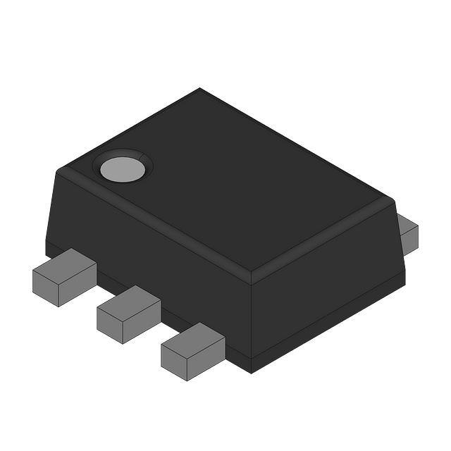
The device is housed in the SOT−89−5 and HSON−6 packages.
Standard voltage versions are 0.8 V, 1.0 V, 1.2 V, 2.5 V, 3.3 V for fixed
version and adjustable output voltage down to 1.0 V.
http://onsemi.com
MARKING
DIAGRAMS
1
XXX
XMM
G
SOT−89−5
CASE 528AB
Features
• Maximum Operating Voltage of 6.0 V
• Minimum Output Voltage Down to 0.8 V for Fix Version and 1.0 V
•
•
•
•
•
for Adjustable Version
Load Regulation −3 mV at 1 A Output Current
Low Dropout
Build−in Auto Discharge Function for D Version
Standby Mode With Low Consumption
These are Pb−Free Devices
6
1
HSON−6
CASE 506AE
June, 2011 − Rev. 2
1
For actual marking Pb−Free indicator, “G” or microdot “G” may or may not be provided.
Battery Powered Instruments
Hand−Held Instruments
Camcorders and Cameras
Portable communication equipments
© Semiconductor Components Industries, LLC, 2011
XXX
XYYG
XXXX
= Specific Device Code
MM, YY = Lot Number
G or G
= Pb−Free Package
Typical Applications
•
•
•
•
6
ORDERING INFORMATION
See detailed ordering and shipping information in the package
dimensions section on page 15 of this data sheet.
1
Publication Order Number:
NCP694/D
�NCP694
6 5 4
4 5 6
HSON−6
1 2 3
(TOP VIEW)
5
3 2 1
(BOTTOM VIEW)
4
4
5
SOT−89−5
1
2
3
(TOP VIEW)
3
2
1
(BOTTOM VIEW)
Figure 1. Pin Description
PIN FUNCTION DESCRIPTION FOR SOT−89−5 PACKAGE
Pin No.
Pin Name
Description
1
ADJ/NC
2
GND
3
CE
This input is used to place the device into low−power standby. When this input is pulled low, the
device is disabled. If this function is not used, Enable should be connected to Vin.
4
Vin
Positive power supply input voltage.
5
Vout
Regulated output voltage.
Adjust pin for NCP694DADJHT1G and NCP694HADJHT1G / No connection
Power supply ground
PIN FUNCTION DESCRIPTION FOR HSON−6 PACKAGE
Pin No.
Pin Name
1
Vout
Regulated output voltage
Description
2
Vout
Regulated output voltage
3
ADJ / NC
4
GND
5
CE
This input is used to place the device into low power standby. When this input is pulled low, the
device is disabled. If this function is not used, Enable should be connected to Vin.
6
Vin
Positive power supply input voltage
Adjust pin for NCP694DSANADJT1G and NCP694HSANADJT1G / No connection
Power supply ground
Vin
Vout
Vin
Vout
Vin
Vout
Vin
Vout
Vref
CE
Vref
Current Limit&
Thermal Shutdown
CE
Current Limit&
Thermal Shutdown
GND
GND
Version H (NCP694HxxxxT1G)
Version D (NCP694DxxxxT1G)
Figure 2. Internal Block Diagram
http://onsemi.com
2
�NCP694
MAXIMUM RATINGS
Symbol
Value
Unit
Input Voltage
Rating
Vin
6.5
V
Enable Voltage
VCE
−0.3 to Vin
V
Output Voltage
Vout
−0.3 to Vin + 0.3
V
Power Dissipation SOT−89−5
PD
900
mW
Power Dissipation HSON−6
PD
900
mW
Operating Junction Temperature
TJ
+150
°C
Operating Ambient Temperature
TA
−40 to +85
°C
Storage Temperature
Tstg
−55 to +125
°C
Stresses exceeding Maximum Ratings may damage the device. Maximum Ratings are stress ratings only. Functional operation above the
Recommended Operating Conditions is not implied. Extended exposure to stresses above the Recommended Operating Conditions may affect
device reliability.
1. This device series contains ESD protection and exceeds the following tests:
Human Body Model 2000 V per JEDEC
Machine Model Method 200 V
THERMAL CHARACTERISTICS
Rating
Junction−to−Ambient SOT−89−5
Power Dissipation SOT−89−5
Junction−to−Ambient HSON−6
Power Dissipation HSON−6
NOTE:
Symbol
Test Conditions
Typical Value
Unit
RqJA
1 oz Copper Thickness, 100 mm2
111
°C/W
900
mW
111
°C/W
900
mW
PD
RqJA
1 oz Copper Thickness, 100
PD
mm2
Single component mounted on an 80 x 80 x 1.5 mm FR4 PCB with stated copper head spreading area. Using the following
boundary conditions as stated in EIA/JESD 51−1, 2, 3, 7, 12.
http://onsemi.com
3
�NCP694
ELECTRICAL CHARACTERISTICS FOR FIX VERSION (Vin = Vout(nom.) + 1.0 V, VCE = Vin, Cin = 4.7 mF, Cout = 4.7 mF, TA =
25°C, unless otherwise noted)
Characteristic
Symbol
Min
Typ
Max
0.770
0.970
1.170
2.450
3.234
0.8
1.0
1.2
2.5
3.3
0.830
1.030
1.030
2.550
3.366
Output Voltage (TA = 25°C, Iout = 100 mA, Vin−Vout = 1 V)
0.8 V
1.0 V
1.2 V
2.5 V
3.3 V
Vout
Output Current (Vin−Vout = 1 V)
Iout
Input voltage
Vin
1.4
Regline
−
Load Regulation (Iout = 1 mA to 300 mA, Vin = Vout + 2.0 V)
Regload03
Load Regulation (Iout = 1 mA to 1 A, Vin = Vout + 2.0 V)
Regload1
Supply Current (Iout = 0 A, (Vin − Vout) = 1 V, VCE = Vin)
1
Unit
V
A
6.0
V
0.05
0.2
%/V
−15
−2
15
mV
−
−3
−
mV
Iss
60
100
mA
Istby
0.1
1.0
mA
Short Current Limit (Vout = 0 V)
Ish
250
Output Voltage Temperature Coefficient
Tc
Line Regulation (Iout = 100 mA)
Standby Current (VCE = 0V, Vin = 6.0 V)
Enable Input Threshold Voltage
(Voltage Increasing, Output Turns On, Logic High)
(Voltage Decreasing, Output Turns Off, Logic Low)
VthCE
Enable Pull−down Current
Drop Output Voltage (TA = 25°C, Iout = 300 mA)
0.8 V Output voltage Vout (V)
1.0 V
1.2 V
2.5 V
3.3 V
Vin−Vout
Drop Output Voltage (TA = 25°C, Iout = 1A)
0.8 V Output voltage Vout (V)
1.0 V
1.2 V
2.5 V
3.3 V
Vin−Vout
mA
−
$100
−
1.0
0
−
−
6
0.4
100
220
0.33
0.22
0.18
0.10
0.05
0.570
0.470
0.320
0.150
0.100
0.72
0.64
0.56
0.32
0.18
ppm/°C
V
nA
V
V
Ripple Rejection (Ripple 200 mVpp, Iout =100 mA, f = 1 kHz)
PSRR
70
dB
Output Noise (BW = 10 Hz to 100 kHz, Iout = 1 mA)
Vnoise
30
mVrms
Tshd/Hyst
150/30
°C
RDS(on)
30
W
Thermal Shutdown Temperature/Hysteresis
RDS(on) of additional output transistor (D version only)
2. Maximum package power dissipation limits must be observed.
3. Low duty cycle pulse techniques are used during testing to maintain the junction temperature as close to ambient as possible.
http://onsemi.com
4
�NCP694
ELECTRICAL CHARACTERISTIC FOR ADJUSTABLE VERSION (Vin = Vout + 1 V, VCE = Vin, Cin = Cout = 4.7 mF, TA
= 25°C, unless otherwise noted)
Symbol
Min
Input Voltage
Vin
1.4
Supply Current (Vout = VADJ, Vin = 2 V, VCE = Vin)
ISS
Istandby
Characteristic
Standby Current (Vin = 6.0 V, VCE = 0 V)
Reference Voltage For Adjustable Voltage Regulator (Vout = VADJ, Vin = 2.0 V,
Iout = 100 mA
Output Voltage Range
Output Current (Vout = VADJ, Vin = 2.0 V)
Load Regulation (Vin = 1.4 V, 1 mA < Iout < 300 mA, Vout = VADJ)
Vref
0.97
Voutrange
1
Iout
1
Vout/Iout
−15
Typ
Max
Unit
6
V
60
100
uA
0.1
1
uA
1
1.03
V
Vin
V
A
−2
15
mV
Load Regulation (Vin = 1.7 V, 1 mA < Iout < 1 A, Vout = VADJ)
Vout/Iout
−3
Dropout Voltage (Vout = VADJ, Iout = 300 mA)
Vdrop300
0.18
mV
Dropout Voltage (Vout = VADJ, Iout = 1 A)
Vdrop1
0.56
Line regulation (Vout = VADJ, Iout = 100 mA, 1.5 V < Vin < 6.0 V
Vout/Vin
0.05
PSRR ( f = 1 kHz, Vout = VADJ, Vin = 2.5 V, Iout = 100 mA, Input Ripple 0.5 Vpp)
PSRR
70
dB
Output Voltage Temperature Coefficient (Iout = 100 mA, −40°C < TJ < 85°C)
Vout/TJ
$100
ppm/°C
Short Current Limit (Vout = VADJ = 0)
Ilim
250
Enable Pull−down Current
ICE
100
220
−
−
6
0.4
0.32
V
V
0.2
%V
mA
nA
Enable Input Threshold Voltage
(Voltage Increasing, Output Turns On, Logic High)
(Voltage Decreasing, Output Turns Off, Logic Low)
VthCE
Thermal Shutdown Temperature/Hysteresis
Tshdn/
Hyst
150/
30
°C
RDS(on)
30
W
RDS(on) of additional output transistor (D version only)
http://onsemi.com
5
1
0
V
�NCP694
APPLICATIONS INFORMATION
Set external components, especially the output capacitor,
as close as possible to the circuit, and make leads as short as
possible.
A typical application circuit for the NCP694 series is
shown in Figure 5, Typical Application Schematic.
Input Decoupling (C1)
A 4.7 mF capacitor either ceramic or tantalum is
recommended and should be connected as close as possible
to the pins of NCP694 device. Higher values and lower ESR
will improve the overall line transient response.
Thermal
As power across the NCP694 increases, it might become
necessary to provide some thermal relief. The maximum
power dissipation supported by the device is dependent
upon board design and layout. Mounting pad configuration
on the PCB, the board material, and also the ambient
temperature effect the rate of temperature rise for the part.
This is stating that when the NCP694 has good thermal
conductivity through the PCB, the junction temperature will
be relatively low with high power dissipation applications.
Output Decoupling (C2)
The minimum decoupling value is 4.7 mF and can be
augmented to fulfill stringent load transient requirements.
The regulator accepts ceramic chip capacitors as well as
tantalum devices. If a tantalum capacitor is used, and its ESR
is large, the loop oscillation may result. Because of this,
select C2 carefully considering its frequency characteristics.
Larger values improve noise rejection and load regulation
transient response.
Output Voltage Setting of Adjustable Version.
An external two resistors are required for setting desired
output voltage as shows Figure 3. Output Voltage Setting.
The equation for the output voltage is mentioned in equation
below.
Enable Operation
The enable pin CE will turn on or off the regulator. These
limits of threshold are covered in the electrical specification
section of this data sheet. If the enable is not used then the
pin should be connected to Vin. The D version devices
(NCP694DxxxxT1G) have additional circuitry in order to
reach the turn−off speed faster than normal type. When the
mode is into standby with CE signal, auto discharge
transistor turns on.
V out + V ref ) R1 @ I1
+ V ref ) R1 @ ǒI adj ) I2Ǔ
+ V ref ) R1 @ ǒV refńR adjǓ ) R1 @ ǒV refńR2Ǔ
ǒ
Ǔ
+ 1.0 @ ǒ1 ) ǒR1ńR adjǓ ) ǒR1ńR2ǓǓ
+ V ref @ 1 ) ǒR1ńR adjǓ ) ǒR1ńR2Ǔ
Hints
For better accuracy, choosing R2