NCP700B
LDO Regulator - Ultra Low
Noise, High PSRR,
BiCMOS RF
200 mA
Noise sensitive RF applications such as Power Amplifiers in cell
phones and precision instrumentation require very clean power
supplies. The NCP700B is 200 mA LDO that provides the engineer
with a very stable, accurate voltage with ultra low noise and very high
Power Supply Rejection Ratio (PSRR) suitable for RF applications. In
order to optimize performance for battery operated portable
applications, the NCP700B employs an advanced BiCMOS process to
combine the benefits of low noise and superior dynamic performance
of bipolar elements with very low ground current consumption at full
loads offered by CMOS.
Furthermore, in order to provide a small footprint for space
constrained applications, the NCP700B is stable with small, low value
capacitors and is available in a very small WDFN6 1.5 mm x 1.5 mm
and TSOP−5 package.
Features
• Output Voltage Options:
1.8 V, 2.5 V, 2.8 V, 3.0 V, 3.3 V
Contact Factory for Other Voltage Options
Excellent Line and Load Regulation
Ultra Low Noise (typ. 10 mVrms)
Very High PSRR (typ 82 dB @ 1 kHz)
Stable with Ceramic Output Capacitors as low as 1 mF
Very Low Ground Current (typ. 70 mA @ no load)
Low Disable Mode Current (max. 1 mA)
Active Discharge Circuit
Current Limit Protection
Thermal Shutdown Protection
These are Pb−Free Devices
♦
•
•
•
•
•
•
•
•
•
•
♦
MARKING
DIAGRAM
1
WDFN6
CASE 511BJ
XM
G
5
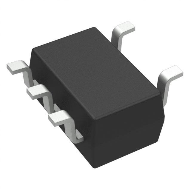
TSOP−5
SN SUFFIX
CASE 483
5
1
XXXAYW
G
1
X, XXX = Specific Device Code
M
= Date Code
A
= Assembly Location
Y
= Year
W
= Work Week
G
= Pb−Free Package
PIN CONNECTIONS
IN
1
6
EN
GND
2
5
NC
OUT
3
4
BYP
(Top View)
Applications
•
•
•
•
•
http://onsemi.com
Smartphones / PDAs / Palmtops / GPS
Cellular Telephones (Power Amplifier)
Noise Sensitive Applications (RF, Video, Audio)
Analog Power Supplies
Battery Supplied Devices
IN
1
GND
2
EN
3
5
OUT
4
BYP
(Top View)
ORDERING INFORMATION
See detailed ordering and shipping information in the package
dimensions section on page 19 of this data sheet.
© Semiconductor Components Industries, LLC, 2013
September, 2019 − Rev. 2
1
Publication Order Number:
NCP700B/D
�NCP700B
VIN
1
6
IN
NCP700B
EN
ON
CIN
1 mF
OUT
BYP
VOUT
3
4
GND
OFF
Cnoise
10 nF
2
COUT
1 mF
Figure 1. NCP700B Typical Application (WDFN6)
RDIS
RPD
Figure 2. Simplified Block Diagram
PIN FUNCTION DESCRIPTION
WDFN
Pin No.
TSSOP−5
Pin No.
Pin Name
1
1
IN
2
2
GND
Power Supply Ground
3
5
OUT
Regulated Output Voltage
4
4
BYP
Noise reduction pin. (Connect 10 nF or 100 nF capacitor to GND)
6
3
EN
Enable pin: This pin allows on/off control of the regulator. To disable the device, connect to
GND. If this function is not in use, connect to Vin. Internal 5 MW Pull Down resistor is connected between EN and GND.
5
-
N/C
Not connected
Description
Input Voltage
http://onsemi.com
2
�NCP700B
MAXIMUM RATINGS
Symbol
Value
Unit
Input Voltage
Rating
IN
−0.3 V to 6 V
V
Chip Enable Voltage
EN
−0.3 V to VIN +0.3 V
Noise Reduction Voltage
BYP
−0.3 V to VIN +0.3 V
V
Output Voltage
OUT
−0.3 V to VIN +0.3 V
V
Output short−circuit duration
Infinity
Maximum Junction Temperature
Storage Temperature Range
Electrostatic Discharge (Note 1)
Human Body Model
TJ(max)
150
°C
TSTG
−55 to 150
°C
ESD
2000
V
Machine Model
200
Stresses exceeding Maximum Ratings may damage the device. Maximum Ratings are stress ratings only. Functional operation above the
Recommended Operating Conditions is not implied. Extended exposure to stresses above the Recommended Operating Conditions may
affect device reliability.
1. This device series contains ESD protection and exceeds the following tests:
Human Body Model 2000 V tested per MIL−STD−883, Method 3015
Machine Model Method 200 V
THERMAL CHARACTERISTICS
Rating
Symbol
Value
Package Thermal Resistance, WDFN6: (Note 2)
Junction−to−Ambient (Note 3)
Package Thermal Characterization Parameter, WDFN6:
Junction-to-Lead (Pin 2) (Note 3)
Junction-to-Board (Note 3)
qJA
185
YJL2
YJB
123
111
Package Thermal Resistance, TSOP-5: (Note 2 and 3)
Junction−to−Case (Pin 2)
Junction−to−Ambient
YJL2
RqJA
92
204
2. Refer to APPLICATION INFORMATION for Safe Operating Area
3. Single component mounted on 1 oz, FR4 PCB with 645mm2 Cu area.
http://onsemi.com
3
Unit
°C/W
°C/W
�NCP700B
ELECTRICAL CHARACTERISTICS VIN = VOUT + 0.5 V or 2.5 V (whichever is greater), VEN = 1.2 V, CIN = COUT = 1 mF, Cnoise =
10 nF, IOUT = 1 mA, TJ = −40°C to 125°C, unless otherwise specified (Note 4)
Parameter
Test Conditions
Symbol
Min
Typ
Max
Unit
VIN
2.5
−
5.5
V
TJ = −40°C to 125°C,
VIN = (VOUT + 0.5 V) to 5.5 V
IOUT = 1 mA to 200 mA
VOUT
−2.5%
−
+2.5%
V
Line Regulation
VIN = (VOUT +0.5 V) to 5.5 V, IOUT = 1 mA
DVOUT /
DVIN
−
0.6
4
mV
Load Regulation
IOUT = 0 mA to 200 mA
DVOUT /
DIOUT
−
0.2
5
mV
VDO
−
−
−
−
140
120
115
110
230
205
190
185
mV
VOUT = VOUT(NOM) – 0.1 V
ILIM
200
310
470
mA
VOUT = 0V
ISC
205
320
490
mA
−
−
70
75
110
130
REGULATOR OUTPUT
Input Voltage Range
Output Voltage Accuracy
Dropout Voltage (Note 5)
IOUT= 200 mA
Output Current Limit
Output Short Circuit Current
Ground Current
IOUT = 0 mA
IOUT = 200 mA
Disable Current
Power Supply Rejection Ratio
Output Noise Voltage
Thermal Shutdown
mA
IDIS
−
0.1
1
mA
VIN = VOUT +1.0 V, VOUT = 1.8 V,
IOUT = 150 mA, f = 1 kHz
PSRR
−
82
−
dB
VN
−
−
15
10
−
−
mVRMS
Cnoise = 10 nF
Cnoise = 100 nF
IOUT = 150 mA, Cnoise = 10 nF
tON
−
400
−
ms
Vth(EN)
−
1.2
−
−
0.4
−
V
RPD
2.5
5
10
MW
VEN = 0 V
RDIS
−
1
−
kW
Shutdown, Temperature increasing
TSDU
−
150
−
°C
Reset, Temperature decreasing
TSDD
−
135
−
°C
TJ
−40
125
°C
Low
High
Enable Internal Pull−Down
Resistance (Note 7)
Active Discharge Resistance
IGND
VEN = 0 V
f = 10 Hz to 100 kHz,
IOUT = 150 mA,
VOUT = 1.8 V
Turn−On Time (Note 6)
Enable Threshold
VOUT(NOM) = 2.5 V
VOUT(NOM) = 2.8 V
VOUT(NOM) = 3.0 V
VOUT(NOM) = 3.3 V
Operating Junction Temperature
4. Performance guaranteed over the indicated operating temperature range by design and/or characterization tested at TJ = TA = 25°C. Low
duty cycle pulse techniques are used during testing to maintain the junction temperature as close to ambient as possible.
5. Measured when the output voltage falls 100 mV below the nominal output voltage (nominal output voltage is the voltage at the output measured under the condition VIN = VOUT + 0.5 V). In the case of devices having the nominal output voltage VOUT = 1.8 V the minimum input
to output voltage differential is given by the VIN(MIN) = 2.5 V.
6. The turn−on time is the time from asserting the EN to the point where output voltage reaches 98% nominal voltage level.
7. Expected to disable the device when EN pin is floating.
http://onsemi.com
4
�NCP700B
TYPICAL CHARACTERISTICS
Vout, OUTPUT VOLTAGE (V)
1.836
1.824
1.812
1.800
1.788
VIN = 2.5 V,
CIN = COUT = 1 mF,
Cnoise = 10 nF
1.776
1.764
−40
−20
0
20
40
60
80
100
120
TJ, JUNCTION TEMPERATURE (°C)
Figure 3. Output Voltage vs. Junction
Temperature, VOUT = 1.8 V
Vout, OUTPUT VOLTAGE (V)
2.8560
2.8373
2.8187
2.8000
2.7813
VIN = 3.3 V,
CIN = COUT = 1 mF,
Cnoise = 10 nF
2.7627
2.7440
−40
−20
0
20
40
60
80
100
120
TJ, JUNCTION TEMPERATURE (°C)
Figure 4. Output Voltage vs. Junction
Temperature, VOUT = 2.8 V
Vout, OUTPUT VOLTAGE (V)
3.06
3.04
3.02
3.00
2.98
VIN = 3.5 V,
CIN = COUT = 1 mF,
Cnoise = 10 nF
2.96
2.94
−40
−20
0
20
40
60
80
TJ, JUNCTION TEMPERATURE (°C)
100
Figure 5. Output Voltage vs. Junction
Temperature, VOUT = 3.0 V
http://onsemi.com
5
120
�NCP700B
TYPICAL CHARACTERISTICS
180
VDO, DROPOUT VOLTAGE (mV)
Vout, OUTPUT VOLTAGE (V)
3.3660
3.3440
3.3220
3.3000
3.2780
VIN = 3.8 V,
CIN = COUT = 1 mF,
Cnoise = 10 nF
3.2560
3.2340
−40
−20
0
20
40
60
80
100
CIN = COUT = 1 mF,
Cnoise = 10 nF
150
TJ = 25°C
120
TJ = 125°C
90
60
TJ = −40°C
30
0
0
120
40
TJ, JUNCTION TEMPERATURE (°C)
90
180
CIN = COUT = 1 mF,
Cnoise = 10 nF
120
TJ = 25°C
TJ = 125°C
60
TJ = −40°C
30
0
0
40
80
120
160
160
200
Figure 7. Dropout Voltage vs. Output Current,
VOUT = 2.8 V
VDO, DROPOUT VOLTAGE (mV)
VDO, DROPOUT VOLTAGE (mV)
150
120
IOUT, OUTPUT CURRENT (mA)
Figure 6. Output Voltage vs. Junction
Temperature, VOUT = 3.3 V
180
80
200
150
CIN = COUT = 1 mF,
Cnoise = 10 nF
120
TJ = 25°C
90
TJ = 125°C
60
TJ = −40°C
30
0
0
40
80
120
160
200
IOUT, OUTPUT CURRENT (mA)
IOUT, OUTPUT CURRENT (mA)
Figure 8. Dropout Voltage vs. Output Current,
VOUT = 3.0 V
Figure 9. Dropout Voltage vs. Output Current,
VOUT = 3.3 V
http://onsemi.com
6
�NCP700B
TYPICAL CHARACTERISTICS
100
110
90
90
80
80
IOUT = 150 mA
60
PSRR (dB)
PSRR (dB)
70
IOUT = 200 mA
50
40
TA = 25°C,
Cnoise = 10 nF,
COUT = 1 mF,
VOUT = 1.8 V,
VIN = 3.0 VDC ± 50 mVAC
30
20
10
0
IOUT = 10 mA
100
IOUT = 10 mA
10
100
IOUT = 150 mA
70
60
IOUT = 200 mA
50
40
TA = 25°C,
Cnoise = 100 nF,
20 COUT = 1 mF,
10 VOUT = 1.8 V,
VIN = 3.0 VDC ± 50 mVAC
0
10
100
1k
10k
FREQUENCY (Hz)
30
1k
10k
FREQUENCY (Hz)
100k
1M
Figure 10. PSRR vs. Frequency, 1.8 V Output
Voltage Option, COUT = 1 mF, Cnoise = 10 nF
120
110
IOUT = 10 mA
90
90
80
70
IOUT = 150 mA
60
PSRR (dB)
PSRR (dB)
IOUT = 10 mA
100
80
IOUT = 200 mA
50
40
TA = 25°C,
Cnoise = 10 nF,
COUT = 4.7 mF,
VOUT = 1.8 V,
VIN = 3.0 VDC ± 50 mVAC
30
20
10
10
100
IOUT = 150 mA
70
60
IOUT = 200 mA
50
40
TA = 25°C,
Cnoise = 100 nF,
20 COUT = 4.7 mF,
10 VOUT = 1.8 V,
VIN = 3.0 VDC ± 50 mVAC
0
10
100
1k
10k
FREQUENCY (Hz)
30
1k
10k
FREQUENCY (Hz)
100k
1M
Figure 12. PSRR vs. Frequency, 1.8 V Output
Voltage Option, COUT = 4.7 mF, Cnoise = 10 nF
110
100
90
70
60
IOUT = 200 mA
50
40
TA = 25°C,
Cnoise = 10 nF,
COUT = 1 mF,
VOUT = 2.8 V,
VIN = 3.3 VDC ± 50 mVAC
30
20
10
10
100
1k
IOUT = 150 mA
80
IOUT = 150 mA
PSRR (dB)
PSRR (dB)
80
70
IOUT = 200 mA
60
50
40
TA = 25°C,
Cnoise = 100 nF,
COUT = 1 mF,
VOUT = 2.8 V,
VIN = 3.3 VDC ± 50 mVAC
30
20
10
10k
100k
1M
IOUT = 10 mA
100
IOUT = 10 mA
90
100k
Figure 13. PSRR vs. Frequency, 1.8V Output
Voltage Option, COUT = 4.7mF, Cnoise = 100nF
110
0
1M
Figure 11. PSRR vs. Frequency, 1.8 V Output
Voltage Option, COUT = 1mF, Cnoise = 100nF
100
0
100k
0
1M
FREQUENCY (Hz)
10
1k
10k
FREQUENCY (Hz)
Figure 14. PSRR vs. Frequency, 2.8 V Output
Voltage Option, COUT = 1 mF, Cnoise = 10 nF
Figure 15. PSRR vs. Frequency, 2.8 V Output
Voltage Option, COUT = 1 mF, Cnoise = 100 nF
http://onsemi.com
7
100
100k
1M
�NCP700B
TYPICAL CHARACTERISTICS
110
110
100
100
IOUT = 10 mA
90
90
80
70
60
IOUT = 200 mA
50
40
30
20
10
0
10
OUTPUT VOLTAGE NOISE (mV/√HZ)
TA = 25°C,
Cnoise = 10 nF,
COUT = 4.7 mF,
VOUT = 2.8 V,
VIN = 3.3 VDC ± 50 mVAC
100
1k
IOUT = 200 mA
50
40
TA = 25°C,
Cnoise = 100 nF,
COUT = 4.7 mF,
VOUT = 2.8 V,
VIN = 3.3 VDC ± 50 mVAC
10
10k
100k
0
1M
10
100
1k
10k
100k
1M
FREQUENCY (Hz)
FREQUENCY (Hz)
Figure 16. PSRR vs. Frequency, 2.8 V Output
Voltage Option, COUT = 4.7 mF, Cnoise = 10 nF
Figure 17. PSRR vs. Frequency, 2.8 V Output
Voltage Option, COUT = 4.7 mF, Cnoise = 100 nF
10
VOUT = 2.8 V
10 Hz − 100 kHz Integral
Noise: Vn = 22.6 mVrms
1.0
0.01
10
60
20
VOUT = 3.3 V
10 Hz − 100 kHz Integral
Noise: Vn = 25.3 mVrms
0.10
IOUT = 150 mA
70
30
OUTPUT VOLTAGE NOISE (mV/√HZ)
OUTPUT VOLTAGE NOISE (mV/√HZ)
10
1.0
PSRR (dB)
IOUT = 150 mA
IOUT = 50 mA,
COUT = 1 mF,
Cnoise = 10 nF
VIN = VOUT = +0.5 V or
2.5 V, whichever is higher
100
1k
VOUT = 1.8 V
10 Hz − 100 kHz Integral
Noise: Vn = 14.9 mVrms
10k
100k
1M
VOUT = 3.3 V
10 Hz − 100 kHz Integral
Noise: Vn = 11.9 mVrms
1.0
IOUT = 50 mA,
COUT = 1 mF,
Cnoise = 100 nF
VIN = VOUT = +0.5 V or
2.5 V, whichever is higher
VOUT = 2.8 V
10 Hz − 100 kHz Integral
Noise: Vn = 11.7 mVrms
0.10
0.01
VOUT = 1.8 V
10 Hz − 100 kHz Integral
Noise: Vn = 9.4 mVrms
10
100
1k
10k
100k
1M
FREQUENCY (Hz)
FREQUENCY (Hz)
Figure 18. Output Noise vs. Frequency, COUT =
1 mF, Cnoise = 10 nF, IOUT = 50 mA
Figure 19. Output Noise vs. Frequency, COUT =
1 mF, Cnoise = 100 nF, IOUT = 50 mA
10
VOUT = 3.3 V
10 Hz − 100 kHz Integral
Noise: Vn = 22.85 mVrms
OUTPUT VOLTAGE NOISE (mV/√HZ)
PSRR (dB)
80
10
IOUT = 10 mA
VOUT = 2.8 V
10 Hz − 100 kHz Integral
Noise: Vn = 22.7 mVrms
VOUT = 1.8 V
10 Hz − 100 kHz Integral
Noise: Vn = 15 mVrms
0.10 I
OUT = 200 mA,
COUT = 1 mF,
Cnoise = 10 nF
VIN = VOUT = +0.5 V or
2.5 V, whichever is higher
0.01
10
100
1k
10k
FREQUENCY (Hz)
100k
1M
VOUT = 3.3 V
10 Hz − 100 kHz Integral
Noise: Vn = 12 mVrms
1.0
VOUT = 2.8 V
10 Hz − 100 kHz Integral
Noise: Vn = 11.7 mVrms
0.10
0.01
IOUT = 200 mA,
COUT = 1 mF,
Cnoise = 100 nF
VIN = VOUT = +0.5 V or
2.5 V, whichever is higher
VOUT = 1.8 V
10 Hz − 100 kHz Integral
Noise: Vn = 9.5 mVrms
10
Figure 20. Output Noise vs. Frequency, COUT =
1 mF, Cnoise = 10 nF, IOUT = 200 mA
100
1k
10k
FREQUENCY (Hz)
100k
1M
Figure 21. Output Noise vs. Frequency, COUT =
1 mF, Cnoise = 100 nF, IOUT = 200 mA
http://onsemi.com
8
�NCP700B
TYPICAL CHARACTERISTICS
TA = 25°C,
COUT = 1 mF,
VOUT = 3.3 V,
IOUT = 200 mA
VIN = 3.8 V
30
25
20
15
10
0
50
18
16
14
12
10
8
4
2
0
100 150 200 250 300 350 400 450 500
Cnoise, NOISE BYPASS CAPACITOR (nF)
TA = 25°C,
Cnoise = 100 nF,
VOUT = 3.3 V,
IOUT = 200 mA
VIN = 3.8 V
6
1
Figure 22. Output Noise vs. Noise Bypass
Capacitance, COUT = 1 mF, VOUT = 3.3 V, IOUT =
200 mA
19
21
15
26
VOUT = 3.3 V
24
VOUT = 2.8 V
10 HZ to 100 kHz RMS OUTPUT
NOISE (mVrms)
28
22
20
18
16
VOUT = 1.8 V
14
TA = 25°C, Cnoise = 10 nF, COUT = 1 mF,
VIN = VOUT + 0.5 V or 2.5 V, whichever is higher
12
0
25
50
75
100
125
150
IOUT, OUTPUT CURRENT (mA)
175
14
13
VOUT = 2.8 V
11
10
9
VOUT = 1.8 V
8
7
TA = 25°C, Cnoise = 100 nF, COUT = 1 mF,
VIN = VOUT + 0.5 V or 2.5 V, whichever is higher
6
5
200
VOUT = 3.3 V
12
0
Figure 24. Output Noise vs. Load Current,
Cnoise = 10 nF, COUT = 1 mF
25
50
75
100
125
150
IOUT, OUTPUT CURRENT (mA)
200
200 mA
1 mA
100
0
1.85
1.80
1.75
1.70
COUT = 4.7 mF, VIN = 2.5 V, Cnoise = 100 nF,
dIOUT/dt = 200 mA / 1 ms
1.65
1.60
0
40
80
175
Figure 25. Output Noise vs. Load Current,
Cnoise = 100 nF, COUT = 1 mF
300
VOUT, OUTPUT VOLTAGE (V)
10 HZ to 100 kHz RMS OUTPUT
NOISE (mVrms)
5
7
9
11 13 15 17
COUT, OUTPUT CAPACITOR (mF)
Figure 23. Output Noise vs. Output
Capacitance, Cnoise = 100 nF, VOUT = 3.3 V,
IOUT = 200 mA
30
10
3
120 160 200 240 280 320 360 400
t, TIME (ms)
Figure 26. Load Transient Response, VOUT =
1.8 V, COUT = 4.7 mF, Cnoise = 100 nF
http://onsemi.com
9
IOUT, OUTPUT CURRENT (mA)
5
20
10 HZ to 100 kHz RMS OUTPUT
NOISE (mVrms)
10 HZ to 100 kHz RMS OUTPUT
NOISE (mVrms)
35
200
�NCP700B
TYPICAL CHARACTERISTICS
VOUT, OUTPUT VOLTAGE (V)
200
200 mA
1 mA
100
0
1.90
1.85
1.80
1.75
1.70
COUT = 1 mF, VIN = 2.5 V, Cnoise = 100 nF,
dIOUT/dt = 200 mA / 1 ms
1.65
1.60
0
40
80
IOUT, OUTPUT CURRENT (mA)
300
120 160 200 240 280 320 360 400
t, TIME (ms)
Figure 27. Load Transient Response, VOUT =
1.8 V, COUT = 1 mF, Cnoise = 100 nF
VOUT, OUTPUT VOLTAGE (V)
200
200 mA
1 mA
100
0
3.40
3.35
3.30
3.25
3.20
COUT = 4.7 mF, VIN = 3.8 V, Cnoise = 100 nF,
dIOUT/dt = 200 mA / 1 ms
3.15
3.10
0
40
80
IOUT, OUTPUT CURRENT (mA)
300
120 160 200 240 280 320 360 400
t, TIME (ms)
Figure 28. Load Transient Response, VOUT =
3.3 V, COUT = 4.7 mF, Cnoise = 100 nF
VOUT, OUTPUT VOLTAGE (V)
200
200 mA
1 mA
100
0
3.40
3.35
3.30
3.25
3.20
COUT = 1 mF, VIN = 3.8 V, Cnoise = 100 nF,
dIOUT/dt = 200 mA / 1 ms
3.15
3.10
0
40
80
120 160 200 240 280 320 360 400
t, TIME (ms)
Figure 29. Load Transient Response, VOUT =
3.3 V, COUT = 1 mF, Cnoise = 100 nF
http://onsemi.com
10
IOUT, OUTPUT CURRENT (mA)
300
�NCP700B
TYPICAL CHARACTERISTICS
3.5
VIN = 3.5 V
VIN = 2.5 V
3.0
2.5
1.810
1.805
1.800
1.795
1.790
COUT = 1 mF, VIN = 2.5 V, Cnoise = 100 nF,
IOUT = 30 mA, dVIN/dt = 1 V / 1 ms
1.785
1.780
VIN, INPUT VOLTAGE (V)
VOUT, OUTPUT VOLTAGE (V)
4.0
0
20
40
60
80 100 120 140 160 180 200
t, TIME (ms)
Figure 30. Line Transient Response,
VOUT = 1.8 V, COUT = 1 mF, IOUT = 30 mA
3.5
VIN = 3.5 V
VIN = 2.5 V
3.0
2.5
1.810
1.805
1.800
1.795
COUT = 1 mF, VIN = 2.5 V,
Cnoise = 100 nF, IOUT = 200 mA,
dVIN/dt = 1 V / 1 ms
1.790
1.785
1.780
0
20
40
60
VIN, INPUT VOLTAGE (V)
VOUT, OUTPUT VOLTAGE (V)
4.0
80 100 120 140 160 180 200
t, TIME (ms)
Figure 31. Line Transient Response,
VOUT = 1.8 V, COUT = 1 mF, IOUT = 200 mA
5.0
VIN = 3.5 V
4.0
3.5
3.010
3.005
3.000
2.995
2.990
COUT = 1 mF, VIN = 3.5 V,
Cnoise = 100 nF, IOUT = 30 mA,
dVIN/dt = 1 V / 1 ms
2.985
2.980
0
20
40
60
80 100 120 140 160 180 200
t, TIME (ms)
Figure 32. Line Transient Response,
VOUT = 3.0 V, COUT = 1 mF, IOUT = 30 mA
http://onsemi.com
11
VIN, INPUT VOLTAGE (V)
VOUT, OUTPUT VOLTAGE (V)
4.5
VIN = 4.5 V
�NCP700B
TYPICAL CHARACTERISTICS
4.5
VIN = 4.5 V
4.0
VIN = 3.5 V
3.5
3.010
3.005
3.000
2.995
COUT = 1 mF, VIN = 3.5 V,
Cnoise = 100 nF, IOUT = 200 mA,
dVIN/dt = 1 V / 1 ms
2.990
2.985
2.980
0
20
40
60
VIN, INPUT VOLTAGE (V)
VOUT, OUTPUT VOLTAGE (V)
5.0
80 100 120 140 160 180 200
t, TIME (ms)
Figure 33. Line Transient Response,
VOUT = 3.0 V, COUT = 1 mF, IOUT = 200 mA
3.8
VEN = 3.8 V
1.9
0.0
VEN = 0 V
Cnoise = 10 nF
4.0
3.0
Cnoise = 220 nF
2.0
1.0
Cnoise = 100 nF
COUT = 1 mF,
VIN = 3.8 V
0.0
−1.0
VEN, ENABLE VOLTAGE (V)
VOUT, OUTPUT VOLTAGE (V)
5.7
Cnoise = 47 nF
0
2
4
6
8
10
t, TIME (ms)
12
14
16
Figure 34. Turn−On Response
VOUT = 3.3 V, COUT = 1 mF, IOUT = 30 mA
3.50
VEN = 3.5 V
1.75
0.00
VEN = 0 V
Cnoise = 10 nF
4.0
3.0
Cnoise = 220 nF
2.0
1.0
Cnoise = 100 nF
0.0
−1.0
Cnoise = 47 nF
0
2
4
6
8
10
t, TIME (ms)
COUT = 1 mF,
VIN = 3.5 V
12
14
Figure 35. Turn−On Response
VOUT = 3 V, COUT = 1 mF, IOUT = 30 mA
http://onsemi.com
12
16
VEN, ENABLE VOLTAGE (V)
VOUT, OUTPUT VOLTAGE (V)
5.25
�NCP700B
TYPICAL CHARACTERISTICS
2
VEN = 2.5 V
1
0
VEN = 0 V
Cnoise = 10 nF
2.0
1.5
Cnoise = 220 nF
1.0
0.5
Cnoise = 100 nF
0.0
−0.5
COUT = 1 mF,
VIN = 2.5 V
Cnoise = 47 nF
0
1
2
3
4
5
6
7
8
9
VEN, ENABLE VOLTAGE (V)
VOUT, OUTPUT VOLTAGE (V)
3
10
t, TIME (ms)
Figure 36. Turn−On Response
VOUT = 1.8 V, COUT = 1 mF, IOUT = 30 mA
5.7
Cnoise = 10 nF,
TJ = 25°C
VEN = 0 V
4.0
3.8
1.9
0.0
RRLOAD = 22 W
3.0
RRLOAD = 110 W
2.0
RRLOAD = 3.3 kW
1.0
VEN, ENABLE VOLTAGE (V)
VOUT, OUTPUT VOLTAGE (V)
VEN = 3.8 V
0.0
−1.0
0
1
2
3
4
5
6
t, TIME (ms)
7
8
9
10
Figure 37. Turn−Off Response
VOUT = 3.3 V, COUT = 1 mF
VOUT, OUTPUT VOLTAGE (V)
5.25
3.50
1.75
VEN = 0 V
0.00
RRLOAD = 20 W
3.0
RRLOAD = 100 W
2.0
RRLOAD = 3 kW
1.0
0.0
−1.0
0
1
2
3
4
5
6
t, TIME (ms)
7
8
Figure 38. Turn−Off Response
VOUT = 3 V, COUT = 1 mF
http://onsemi.com
13
9
10
VEN, ENABLE VOLTAGE (V)
Cnoise = 10 nF,
TJ = 25°C
VEN = 3.5 V
�NCP700B
TYPICAL CHARACTERISTICS
1.25
0
RRLOAD = 12 W
1.5
RRLOAD = 60 W
1.0
RRLOAD = 1.8 kW
0.5
tON, TURN−ON TIME (ms)
VEN, ENABLE VOLTAGE (V)
VOUT, OUTPUT VOLTAGE (V)
2.5
VEN = 0 V
2.0
12
3.75
Cnoise = 10 nF,
TJ = 25°C
VEN = 2.5 V
0.0
−0.5
0
1
2
3
4
5
6
t, TIME (ms)
7
8
9
10
8
VOUT = 3.3 V
6
VOUT = 3 V
4
VOUT = 1.8 V
2
0
10
TJ = 25°C,
IOUT = 0 mA − 200 mA
0
Figure 39. Turn−Off Response
VOUT = 1.8 V, COUT = 1 mF
Figure 40. Turn−On Time vs. Noise Bypass
Capacitance, COUT = 1 mF, IOUT = 0 mA −
200 mA
600
400
200
IOUT = 1 mA
4
3
VOUT = 3 V
2
1
VOUT = 0 V
0
−1
0.0
0
Short−Circuit
Normal
Operation
0.1
0.2
0.3
0.4 0.5 0.6
t, TIME (ms)
0.7
0.8
0.9
350
IOUT, OUTPUT CURRENT (mA)
ISC, SHORT−CIRCUIT CURRENT (mA)
VOUT, OUTPUT VOLTAGE (V)
800
IOUT = 1 mA
Cnoise = 100 nF
IOUT = 325 mA
VIN = VOUT + 0.5 V,
CIN = COUT = 1 mF,
Cnoise = 10 nF
333
317
300
283
267
250
−40
1.0
2.00
300
1.75
100
0
0
20
40
60
80
100
TJ, JUNCTION TEMPERATURE (°C)
120
1.50
1.25
TJ = 25°C
1.00
VOUT = 3 V
0.75
2.0
1.0
IOUT = 200 mA
Cnoise = 100 nF
0
−1.0
0.0
IOUT, OUTPUT CURRENT (mA)
VOUT, OUTPUT VOLTAGE (V)
VOUT, OUTPUT VOLTAGE (V)
400
200
Normal
Operation
3.0
−20
Figure 42. Short−Circuit Current vs. Junction
Temperature, VOUT = 1.8 V, 3.3 V
IOUT = 200 mA
4.0
VOUT = 3.3 V
VOUT = 1.8 V
Figure 41. Short−Circuit Protection,
VOUT = 3 V, COUT = 1 mF, Cnoise = 100 nF
Thermal
Shutdown
20 40 60 80 100 120 140 160 180 200 220 240
Cnoise, NOISE BYPASS CAPACITANCE (nF)
1.0
2.0
3.0
4.0
5.0
6.0
7.0
8.0
0.50
TJ = −40°C
0.25
TJ = 125°C
IOUT = 10 mA
Cnoise = 100 nF
2.5
4
0.00
9.0 10.0
0
0.5
1
1.5
2
3
3.5
4.5
5
VIN, INPUT VOLTAGE (V)
VIN, INPUT VOLTAGE (V)
Figure 43. Thermal Shutdown Protection
VOUT = 3 V, Cnoise = 100 nF, COUT = 1 mF
Figure 44. Output Voltage vs. Input Voltage,
VOUT = 1.8 V, COUT = 1 mF
http://onsemi.com
14
5.5
�NCP700B
TYPICAL CHARACTERISTICS
3.50
3.25
3.00
2.75
2.50
2.25
2.00
1.75
1.50
1.25
1.00
0.75
0.50
0.25
0
3.00
2.50
2.25
2.00
1.75
1.50
1.25
1.00
TJ = 25°C
0.75
TJ = −40°C
0.50
0
IOUT = 10 mA
Cnoise = 100 nF
TJ = 125°C
0.25
0
0.5
1
1.5
2
2.5
3
3.5
4
4.5
5
VOUT, OUTPUT VOLTAGE (V)
VOUT, OUTPUT VOLTAGE (V)
2.75
5.5
TJ = 25°C
TJ = −40°C
TJ = 125°C
0
0.5
1
1.5
2
2.5
3
3.5
IOUT = 10 mA
Cnoise = 100 nF
4
4.5
5
VIN, INPUT VOLTAGE (V)
VIN, INPUT VOLTAGE (V)
Figure 45. Output Voltage vs. Input Voltage,
VOUT = 2.8 V, COUT = 1 mF
Figure 46. Output Voltage vs. Input Voltage,
VOUT = 3.3 V, COUT = 1 mF
1.8091
2.8038
VOUT, OUTPUT VOLTAGE (V)
1.8089
1.8088
1.8087
1.8086
1.8085
1.8084
1.8083
1.8082
3
3.5
4
4.5
5
5.5
2.8036
2.8035
2.8034
2.8033
2.8032
2.8031
2.8030
2.8029
2.8028
3
3.5
4
4.5
5
5.5
VIN, INPUT VOLTAGE (V)
VIN, INPUT VOLTAGE (V)
Figure 47. Output Voltage vs. Input Voltage,
VOUT = 1.8 V, COUT = 1 mF
Figure 48. Output Voltage vs. Input Voltage,
VOUT = 2.8 V, COUT = 1 mF
3.3129
90
VOUT, OUTPUT VOLTAGE (V)
3.3127
IQ, QUIESCENT CURRENT (mA)
TJ = 25°C
IOUT = 10 mA
Cnoise = 100 nF
3.3128
3.3126
3.3125
3.3124
3.3123
3.3122
3.3121
3.3120
3.3119
3.5
TJ = 25°C
IOUT = 10 mA
Cnoise = 100 nF
2.8037
VOUT, OUTPUT VOLTAGE (V)
TJ = 25°C
IOUT = 10 mA
Cnoise = 100 nF
1.8090
1.8081
2.5
5.5
4
4.5
5
5.5
80
70
TJ = 125°C
60
50
TJ = 25°C
40
TJ = −40°C
30
20
VOUT = 2.8 V
COUT = 1 mF
10
0
0
0.5
1
1.5
2
2.5
3
3.5
4
4.5
5
VIN, INPUT VOLTAGE (V)
VIN, INPUT VOLTAGE (V)
Figure 49. Output Voltage vs. Input Voltage,
VOUT = 3.3 V, COUT = 1 mF
Figure 50. Quiescent Current vs. Input
Voltage, VOUT = 2.8 V, COUT = 1 mF
http://onsemi.com
15
5.5
�NCP700B
TYPICAL CHARACTERISTICS
100
90
IQ, QUIESCENT CURRENT (mA)
IQ, QUIESCENT CURRENT (mA)
100
TJ = 25°C
80
70
60
TJ = 125°C
50
40
TJ = −40°C
30
20
VOUT = 3.3 V
COUT = 1 mF
10
0
0
0.5
1
1.5
2
2.5
3
3.5
4
4.5
5
TJ = 25°C
70
TJ = −40°C
60
50
40
CIN = COUT = 1 mF,
Cnoise = 10 nF
30
20
40
60
80
100 120 140 160 180 200
VIN, INPUT VOLTAGE (V)
IOUT, OUTPUT CURRENT (mA)
Figure 51. Quiescent Current vs. Input
Voltage, VOUT = 3.3 V, COUT = 1 mF
Figure 52. Quiescent Current vs. Output
Current, VOUT = 3.3 V
90
TJ = 125°C
80
TJ = 25°C
70
TJ = −40°C
IQ, QUIESCENT CURRENT (mA)
IQ, QUIESCENT CURRENT (mA)
80
100
60
50
40
CIN = COUT = 1 mF,
Cnoise = 10 nF
30
20
0
20
40
60
80
TJ = 125°C
80
TJ = 25°C
70
TJ = −40°C
60
50
40
CIN = COUT = 1 mF,
Cnoise = 10 nF
30
20
40
60
80
100 120 140 160 180 200
IOUT, OUTPUT CURRENT (mA)
IOUT, OUTPUT CURRENT (mA)
Figure 53. Quiescent Current vs. Output
Current, VOUT = 3.0 V
Figure 54. Quiescent Current vs. Output
Current, VOUT = 2.8 V
COUT ESR, OUTPUT CAPACITOR (W)
100
TJ = 125°C
90
80
TJ = 25°C
70
TJ = −40°C
60
50
40
CIN = COUT = 1 mF,
Cnoise = 10 nF
30
0
90
20
0
100 120 140 160 180 200
110
IQ, QUIESCENT CURRENT (mA)
TJ = 125°C
20
0
5.5
100
20
90
20
40 60 80 100 120 140 160 180 200
IOUT, OUTPUT CURRENT (mA)
10
Unstable Operation Region
VOUT = 3.3 V
1
VOUT = 2.8 V
VOUT = 1.8 V
Stable Operation Region
0.1
VOUT = 1.8 V, 2.8 V, 3.3 V, CIN = COUT = 1 mF,
Cnoise = 10 nF, VIN = VOUT + 0.5 V or 2.5 V
whichever is higher.
0.01
0
Figure 55. Quiescent Current vs. Output
Current, VOUT = 1.8 V
0.02 0.04 0.06 0.08 0.1
0.12 0.14 0.16 0.18 0.2
IOUT, OUTPUT CURRENT (A)
Figure 56. Output Capacitor ESR vs. Output
Current
http://onsemi.com
16
�NCP700B
APPLICATIONS INFORMATION
General
5 MW pull−down resistor (RPD) assures that the device is
turned off when EN pin is not connected.
The device can be used as a simple regulator without use
of the chip enable feature by tying the EN to the IN pin.
The NCP700B is a high performance 200 mA low
dropout linear regulator. This device delivers excellent noise
and dynamic performance consuming only 75 mA (typ)
quiescent current at full load, with the PSRR of (typ) 82 dB
at 1 kHz. Excellent load transient performance and small
package size makes the device ideal for portable
applications.
Logic EN input provides ON/OFF control of the output
voltage. When the EN is low the device consumes as low as
typically 0.1 mA.
Access to the major contributor of noise within the
integrated circuit – Bandgap Reference is provided through
the BYP pin. This allows bypassing the source of noise by
the noise reduction capacitor and reaching noise levels
below 10 mVRMS.
The device is fully protected in case of output short circuit
condition and overheating assuring a very robust design.
Active Discharge
Active discharge circuitry has been implemented to insure
a fast VOUT turn off time. When EN goes low, the active
discharge transistor turns on creating a path to discharge the
output capacitor COUT through 1 kW (RDIS) resistor.
Turn−On Time
The Turn−On time of the regulator is defined as the time
needed to reach the output voltage which is 98% VOUT after
assertion of the EN pin. This time is determined by the noise
bypass capacitance Cnoise and nominal output voltage level
VOUT according the following formula:
t ON [s] + C noise [F] @
Input Capacitor Requirements (CIN)
V OUT [V]
68 @ 10 −6 [A]
(eq. 1)
Example:
Using Cnoise = 100 nF, VOUT = 3 V, COUT = 1 mF,
It is recommended to connect a 1 mF ceramic capacitor
between IN pin and GND pin of the device. This capacitor
will provide a low impedance path for unwanted AC signals
or noise present on the input voltage. The input capacitor
will also limit the influence of input trace inductances and
Power Supply resistance during sudden load current
changes. Higher capacitances will improve the line transient
response.
t ON + 100 @ 10
−9 @
3
68 @ 10 −6
+ 4.41 ms
The Turn−On time is independent of the load current and
output capacitor COUT. To avoid output voltage overshoot
during Turn−On please select Cnoise ≥ 10 nF.
Current Limit
Output Capacitor Requirements (COUT)
Output Current is internally limited within the IC to a
typical 310 mA. The NCP700B will source this amount of
current measured with a voltage 100 mV lower than the
typical operating output voltage. If the Output Voltage is
directly shorted to ground (VOUT = 0 V), the short circuit
protection will limit the output current to 320 mA (typ). The
current limit and short circuit protection will work properly
up to VIN = 5.5 V at TA = 25°C. There is no limitation for the
short circuit duration.
The NCP700B has been designed to work with low ESR
ceramic capacitors on the output. The device will also work
with other types of capacitors until the minimum value of
capacitance is assured and the capacitor ESR is within the
specified range. Generally it is recommended to use 1 mF or
larger X5R or X7R ceramic capacitor on the output pin.
Noise Bypass Capacitor Requirements (Cnoise)
The Cnoise capacitor is connected directly to the high
impedance node. Any loading on this pin like the connection
of oscilloscope probe, or the Cnoise capacitor leakage will
cause a voltage drop in regulated output voltage. The
minimum value of noise bypass capacitor is 10 nF. Values
below 10 nF should be avoided due to possible Turn−On
overshoot. Particular value should be chosen based on the
output noise requirements (Figure 22). Larger values of
Cnoise will improve the output noise and PSRR but will
increase the regulator Turn−On time.
Thermal Shutdown
When the die temperature exceeds the Thermal Shutdown
threshold (TSDU − 150°C typical), Thermal Shutdown event
is detected and the output (VOUT) is turned off.
The IC will remain in this state until the die temperature
decreases below the Thermal Shutdown Reset threshold
(TSDU − 135°C typical). Once the IC temperature falls below
the 135°C the LDO is turned−on again.
The thermal shutdown feature provides the protection
from a catastrophic device failure due to accidental
overheating. This protection is not intended to be used as a
substitute for proper heat sinking.
Enable Operation
The enable function is controlled by the logic pin EN. The
voltage threshold of this pin is set between 0.4 V and 1.2 V.
Voltage lower than 0.4 V guarantees the device is off.
Voltage higher than 1.2 V guarantees the device is on. The
NCP700B enters a sleep mode when in the off state drawing
less than typically 0.1 mA of quiescent current. The internal
Reverse Current
The PMOS pass transistor has an inherent body diode
which will conduct the current in case that the VOUT > VIN.
http://onsemi.com
17
�NCP700B
15 mVrms by using 10 nF to less than 10 mVrms by using a
100 nF from the BYP pin to ground. For more information
please refer to Figures 22 through 24.
Such condition could exist in the case of pulling the VIN
voltage to ground. Then the output capacitor voltage will be
partially discharged through the PMOS body diode. It have
been verified that the device will not be damaged if the
output capacitance is less than 22 mF. If however larger
output capacitors are used or extended reverse current
condition is anticipated the device may require additional
external protection against the excessive reverse current.
NCP700B does not require any minimum load current for
stability. The minimum load current is assured by the
internal circuitry.
Output Noise
Power Dissipation
Minimum Load Current
For given ambient temperature TA and thermal resistance
RqJA the maximum device power dissipation can be
calculated by:
If we neglect the noise coming from the (IN) input pin of
the LDO, the main contributor of noise present on the output
pin (OUT) is the internal bandgap reference. This is because
any noise which is generated at this node will be
subsequently amplified through the error amplifier and the
PMOS pass device. Access to the bandgap reference node is
supplied through the BYP pin. For the 1.8 V output voltage
option Noise can be reduced from a typical value of
P D(MAX) +
q JA
PD(MAX), TA = 25°C,
2 oz CU Thickness
400
PD(MAX), TA = 25°C,
1 oz CU Thickness
0.7
0.6
300
0.5
250
0.4
200
0.3
150
0.2
qJA, 1 oz CU Thickness
100
0.1
qJA, 2 oz CU Thickness
50
0
100
200
300
400
500
600
PCB COPPER AREA (mm2)
PD(MAX), MAXIMUM POWER
DISSIPATION (W)
0.8
350
0
800
700
Figure 57. Thermal Resistance and Maximum
Power Dissipation vs. Copper Area (WDFN6)
0.60
PD(MAX), TA = 25°C,
2 oz Cu Thickness
290
0.55
270
0.50
250
230
210
0.40
qJA, 1 oz Cu Thickness
190
170
150
0.45
PD(MAX), TA = 25°C,
1 oz Cu Thickness
100
200
300
400
500
PCB COPPER AREA (mm2)
600
0.20
700
Figure 58. Thermal Resistance and Maximum
Power Dissipation vs. Copper Area (TSOP−5)
http://onsemi.com
18
0.30
0.25
qJA, 2 oz Cu Thickness
0
0.35
PD(MAX), MAXIMUM POWER
DISSIPATION (W)
qJA, JUNCTION−TO−AMBIENT
THERMAL RESISTANCE (°C/W)
310
(eq. 2)
For reliable operation junction temperature should be
limited to +125°C.
450
qJA, JUNCTION−TO−AMBIENT
THERMAL RESISTANCE (°C/W)
125 * T A
�NCP700B
Load Regulation
the pin should be as small as possible to avoid noise pickup.
In order to minimize the solution size use 0402 or 0603
capacitors. To obtain small transient variations and good
regulation characteristics place CIN and COUT capacitors
close to the device pins and make the PCB traces wide.
Larger copper area connected to the pins will also improve
the device thermal resistance.
The actual power dissipation can be calculated by the
formula:
The NCP700B features very good load regulation of
5 mV Max. in 0 mA to 200 mA range. In order to achieve
this very good load regulation a special attention to PCB
design is necessary. The trace resistance from the OUT pin
to the point of load can easily approach 100 mW which will
cause 20 mV voltage drop at full load current, deteriorating
the excellent load regulation.
Power Supply Rejection Ratio
The NCP700b features excellent Power Supply Rejection
ratio. The PSRR can be tuned by selecting proper Cnoise and
COUT capacitors.
In the frequency range from 10 Hz up to about 10 kHz the
larger noise bypass capacitor Cnoise will help to improve the
PSRR. At the frequencies above 10 kHz the addition of
higher COUT output capacitor will result in improved PSRR.
P D + ǒV IN * V OUTǓI OUT ) V INI GND
(eq. 3)
Line Regulation
The NCP700B features very good line regulation of
0.6mV/V (typ). Furthermore the detailed Output Voltage vs.
Input Voltage characteristics (Figures 47 through 49) show
that up to VIN = 5 V the Output Voltage deviation is typically
less than 250 mV for 1.8 V output voltage option and less
than 150 mV for higher output voltage options. Above the
VIN = 5 V the output voltage falls rapidly which leads to the
typical 0.6 mV/V.
PCB Layout Recommendations
Connect the input (CIN), output (COUT) and noise bypass
capacitors (Cnoise) as close as possible to the device pins.
The Cnoise capacitor is connected to high impedance BYP
pin and thus the length of the trace between the capacitor and
ORDERING INFORMATION
Device
Nominal Output Voltage
Marking
NCP700BMT18TBG
1.8 V
J
NCP700BMT25TBG
2.5 V
Q
NCP700BMT28TBG
2.8 V
K
NCP700BMT30TBG
3.0 V
L
NCP700BMT33TBG
3.3 V
P
NCP700BSN18T1G
1.8 V
ADQ
NCP700BSN25T1G
2.5 V
AD3
NCP700BSN28T1G
2.8 V
ADR
NCP700BSN30T1G
3.0 V
ADT
NCP700BSN33T1G
3.3 V
ADU
Package
Shipping†
WDFN6
1.5 x 1.5
(Pb−Free)
3000 / Tape & Reel
TSOP-5
(Pb-Free)
3000 / Tape & Reel
†For information on tape and reel specifications, including part orientation and tape sizes, please refer to our Tape and Reel Packaging
Specifications Brochure, BRD8011/D.
http://onsemi.com
19
�MECHANICAL CASE OUTLINE
PACKAGE DIMENSIONS
TSOP−5
CASE 483
ISSUE N
5
1
SCALE 2:1
NOTES:
1. DIMENSIONING AND TOLERANCING PER ASME
Y14.5M, 1994.
2. CONTROLLING DIMENSION: MILLIMETERS.
3. MAXIMUM LEAD THICKNESS INCLUDES LEAD FINISH
THICKNESS. MINIMUM LEAD THICKNESS IS THE
MINIMUM THICKNESS OF BASE MATERIAL.
4. DIMENSIONS A AND B DO NOT INCLUDE MOLD
FLASH, PROTRUSIONS, OR GATE BURRS. MOLD
FLASH, PROTRUSIONS, OR GATE BURRS SHALL NOT
EXCEED 0.15 PER SIDE. DIMENSION A.
5. OPTIONAL CONSTRUCTION: AN ADDITIONAL
TRIMMED LEAD IS ALLOWED IN THIS LOCATION.
TRIMMED LEAD NOT TO EXTEND MORE THAN 0.2
FROM BODY.
D 5X
NOTE 5
2X
DATE 12 AUG 2020
0.20 C A B
0.10 T
M
2X
0.20 T
5
B
1
4
2
B
S
3
K
DETAIL Z
G
A
A
TOP VIEW
DIM
A
B
C
D
G
H
J
K
M
S
DETAIL Z
J
C
0.05
H
C
SIDE VIEW
SEATING
PLANE
END VIEW
GENERIC
MARKING DIAGRAM*
SOLDERING FOOTPRINT*
0.95
0.037
MILLIMETERS
MIN
MAX
2.85
3.15
1.35
1.65
0.90
1.10
0.25
0.50
0.95 BSC
0.01
0.10
0.10
0.26
0.20
0.60
0_
10 _
2.50
3.00
1.9
0.074
5
5
XXXAYWG
G
1
1
Analog
2.4
0.094
XXX = Specific Device Code
A
= Assembly Location
Y
= Year
W = Work Week
G
= Pb−Free Package
1.0
0.039
XXX MG
G
Discrete/Logic
XXX = Specific Device Code
M = Date Code
G
= Pb−Free Package
(Note: Microdot may be in either location)
0.7
0.028
SCALE 10:1
mm Ǔ
ǒinches
*For additional information on our Pb−Free strategy and soldering
details, please download the ON Semiconductor Soldering and
Mounting Techniques Reference Manual, SOLDERRM/D.
DOCUMENT NUMBER:
DESCRIPTION:
98ARB18753C
TSOP−5
*This information is generic. Please refer to
device data sheet for actual part marking.
Pb−Free indicator, “G” or microdot “ G”,
may or may not be present.
Electronic versions are uncontrolled except when accessed directly from the Document Repository.
Printed versions are uncontrolled except when stamped “CONTROLLED COPY” in red.
PAGE 1 OF 1
ON Semiconductor and
are trademarks of Semiconductor Components Industries, LLC dba ON Semiconductor or its subsidiaries in the United States and/or other countries.
ON Semiconductor reserves the right to make changes without further notice to any products herein. ON Semiconductor makes no warranty, representation or guarantee regarding
the suitability of its products for any particular purpose, nor does ON Semiconductor assume any liability arising out of the application or use of any product or circuit, and specifically
disclaims any and all liability, including without limitation special, consequential or incidental damages. ON Semiconductor does not convey any license under its patent rights nor the
rights of others.
© Semiconductor Components Industries, LLC, 2018
www.onsemi.com
�MECHANICAL CASE OUTLINE
PACKAGE DIMENSIONS
WDFN6 1.5x1.5, 0.5P
CASE 511BJ
ISSUE C
DATE 06 OCT 2015
SCALE 4:1
D
L
A
B
NOTES:
1. DIMENSIONING AND TOLERANCING PER
ASME Y14.5M, 1994.
2. CONTROLLING DIMENSION: MILLIMETERS.
3. DIMENSION b APPLIES TO PLATED
TERMINAL AND IS MEASURED BETWEEN
0.15 AND 0.30mm FROM TERMINAL TIP.
4. COPLANARITY APPLIES TO THE EXPOSED
PAD AS WELL AS THE TERMINALS.
L1
DETAIL A
ÍÍÍÍ
ÍÍÍÍ
ÍÍÍÍ
ALTERNATE TERMINAL
CONSTRUCTIONS
E
PIN ONE
REFERENCE
ÉÉÉ
ÉÉÉ
EXPOSED Cu
0.10 C
2X
2X
0.10 C
0.05 C
TOP VIEW
DETAIL B
A3
MOLD CMPD
ÉÉ
ÉÉ
ÇÇ
DIM
A
A1
A3
b
D
E
e
L
L1
L2
A3
A1
DETAIL B
ALTERNATE
CONSTRUCTIONS
GENERIC
MARKING DIAGRAM*
A
0.05 C
1
A1
NOTE 4
C
SIDE VIEW
DETAIL A
e
1
SEATING
PLANE
XXM
G
XX = Specific Device Code
M = Date Code
G
= Pb−Free Package
5X
L
3
MILLIMETERS
MIN
MAX
0.70
0.80
0.00
0.05
0.20 REF
0.20
0.30
1.50 BSC
1.50 BSC
0.50 BSC
0.40
0.60
--0.15
0.50
0.70
*This information is generic. Please refer to
device data sheet for actual part marking.
Pb−Free indicator, “G” or microdot “ G”,
may or may not be present.
L2
RECOMMENDED
MOUNTING FOOTPRINT*
6
4
6X
b
0.10 C A
BOTTOM VIEW
0.05 C
B
6X
0.35
5X
0.73
NOTE 3
1.80
0.83
0.50
PITCH
DIMENSIONS: MILLIMETERS
*For additional information on our Pb−Free strategy and soldering
details, please download the ON Semiconductor Soldering and
Mounting Techniques Reference Manual, SOLDERRM/D.
DOCUMENT NUMBER:
DESCRIPTION:
98AON50296E
WDFN6, 1.5 X 1.5, 0.5 P
Electronic versions are uncontrolled except when accessed directly from the Document Repository.
Printed versions are uncontrolled except when stamped “CONTROLLED COPY” in red.
PAGE 1 OF 1
ON Semiconductor and
are trademarks of Semiconductor Components Industries, LLC dba ON Semiconductor or its subsidiaries in the United States and/or other countries.
ON Semiconductor reserves the right to make changes without further notice to any products herein. ON Semiconductor makes no warranty, representation or guarantee regarding
the suitability of its products for any particular purpose, nor does ON Semiconductor assume any liability arising out of the application or use of any product or circuit, and specifically
disclaims any and all liability, including without limitation special, consequential or incidental damages. ON Semiconductor does not convey any license under its patent rights nor the
rights of others.
© Semiconductor Components Industries, LLC, 2019
www.onsemi.com
�onsemi,
, and other names, marks, and brands are registered and/or common law trademarks of Semiconductor Components Industries, LLC dba “onsemi” or its affiliates
and/or subsidiaries in the United States and/or other countries. onsemi owns the rights to a number of patents, trademarks, copyrights, trade secrets, and other intellectual property.
A listing of onsemi’s product/patent coverage may be accessed at www.onsemi.com/site/pdf/Patent−Marking.pdf. onsemi reserves the right to make changes at any time to any
products or information herein, without notice. The information herein is provided “as−is” and onsemi makes no warranty, representation or guarantee regarding the accuracy of the
information, product features, availability, functionality, or suitability of its products for any particular purpose, nor does onsemi assume any liability arising out of the application or use
of any product or circuit, and specifically disclaims any and all liability, including without limitation special, consequential or incidental damages. Buyer is responsible for its products
and applications using onsemi products, including compliance with all laws, regulations and safety requirements or standards, regardless of any support or applications information
provided by onsemi. “Typical” parameters which may be provided in onsemi data sheets and/or specifications can and do vary in different applications and actual performance may
vary over time. All operating parameters, including “Typicals” must be validated for each customer application by customer’s technical experts. onsemi does not convey any license
under any of its intellectual property rights nor the rights of others. onsemi products are not designed, intended, or authorized for use as a critical component in life support systems
or any FDA Class 3 medical devices or medical devices with a same or similar classification in a foreign jurisdiction or any devices intended for implantation in the human body. Should
Buyer purchase or use onsemi products for any such unintended or unauthorized application, Buyer shall indemnify and hold onsemi and its officers, employees, subsidiaries, affiliates,
and distributors harmless against all claims, costs, damages, and expenses, and reasonable attorney fees arising out of, directly or indirectly, any claim of personal injury or death
associated with such unintended or unauthorized use, even if such claim alleges that onsemi was negligent regarding the design or manufacture of the part. onsemi is an Equal
Opportunity/Affirmative Action Employer. This literature is subject to all applicable copyright laws and is not for resale in any manner.
PUBLICATION ORDERING INFORMATION
LITERATURE FULFILLMENT:
Email Requests to: orderlit@onsemi.com
onsemi Website: www.onsemi.com
◊
TECHNICAL SUPPORT
North American Technical Support:
Voice Mail: 1 800−282−9855 Toll Free USA/Canada
Phone: 011 421 33 790 2910
Europe, Middle East and Africa Technical Support:
Phone: 00421 33 790 2910
For additional information, please contact your local Sales Representative
�