NCP716B
Wide Input Voltage Low
Dropout, Ultra-Low Iq
Regulator
The NCP716B is 150 mA LDO Linear Voltage Regulator. It is a
very stable and accurate device with ultra−low ground current
consumption (4.7 mA over the full output load range) and a wide input
voltage range (up to 24 V). The regulator incorporates several
protection features such as Thermal Shutdown and Current Limiting.
www.onsemi.com
MARKING
DIAGRAM
Features
5
• Operating Input Voltage Range: 2.5 V to 24 V
• Fixed Voltage Options Available:
•
•
•
•
•
•
3.0 V, 3.3 V and 5.0 V
Ultra Low Quiescent Current: Max. 4.7 mA over Temperature
±2% Accuracy over Full Temperature Range
Noise: 115 mVRMS from 200 Hz to 100 kHz
Thermal Shutdown and Current Limit Protection
Available in TSOP−5 Package
This is a Pb−Free Device
5
1
1
XXX = Specific Device Code
A
= Assembly Location
Y
= Year
W = Work Week
G
= Pb−Free Package
(Note: Microdot may be in either location)
PIN CONNECTIONS
Typical Applicaitons
•
•
•
•
XXXAYWG
G
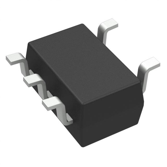
TSOP−5
CASE 483
Portable Equipment
Communication Systems
Industrial Measurement Systems
Home Automation Devices
1
5
N/C
OUT
GND
IN
N/C
TSOP−5
(Top View)
Vout = 3.0V, 3.3 V, 5.0 V/150 mA
Vin= (4 − 24 V)
Vin
NCP716B
Cin
1uF
Vout
Cout
GND
ORDERING INFORMATION
See detailed ordering, marking and shipping information in the
package dimensions section on page 7 of this data sheet.
1uF
Figure 1. Typical Application Schematic
© Semiconductor Components Industries, LLC, 2017
February, 2017 − Rev. 1
1
Publication Order Number:
NCP716B/D
�NCP716B
IN
UVLO
BANDGAP
REFERENCE
THERMAL
SHUTDOWN
MOSFET
DRIVER WITH
CURRENT LIMIT
OUT
EEPROM
GND
Figure 2. Simplified Block Diagram
Table 1. PIN FUNCTION DESCRIPTION
Pin No.
Pin
Name
1
OUT
Regulated output voltage pin. A small 1.0 mF ceramic capacitor is needed from this pin to ground to
assure stability.
2
GND
Power supply ground.
3
IN
4
N/C
No connection. This pin can be tied to ground to improve thermal dissipation or left disconnected.
5
N/C
No connection. This pin can be tied to ground to improve thermal dissipation or left disconnected.
Description
Input pin. A small capacitor is needed from this pin to ground to assure stability.
Table 2. ABSOLUTE MAXIMUM RATINGS
Rating
Symbol
Value
Unit
VIN
−0.3 to 24
V
VOUT
−0.3 to 6
V
tSC
Indefinite
s
TJ(MAX)
150
°C
TSTG
−55 to 150
°C
ESD Capability, Human Body Model (Note 2)
ESDHBM
2000
V
ESD Capability, Machine Model (Note 2)
ESDMM
200
V
Input Voltage (Note 1)
Output Voltage
Output Short Circuit Duration
Maximum Junction Temperature
Storage Temperature
Stresses exceeding those listed in the Maximum Ratings table may damage the device. If any of these limits are exceeded, device functionality
should not be assumed, damage may occur and reliability may be affected.
1. Refer to ELECTRICAL CHARACTERISTICS and APPLICATION INFORMATION for Safe Operating Area.
2. This device series incorporates ESD protection and is tested by the following methods:
ESD Human Body Model tested per EIA/JESD22−A114
ESD Machine Model tested per EIA/JESD22−A115
ESD Charged Device Model tested per EIA/JESD22−C101E
Latchup Current Maximum Rating tested per JEDEC standard: JESD78.
Table 3. THERMAL CHARACTERISTICS
Rating
Thermal Characteristics, TSOP−5
Thermal Resistance, Junction−to−Air
Symbol
Value
Unit
RqJA
250
°C/W
www.onsemi.com
2
�NCP716B
Table 4. ELECTRICAL CHARACTERISTICS Voltage version 3.0 V
−40°C ≤ TJ ≤ 125°C; VIN = 4.0 V; IOUT = 1 mA, CIN = COUT = 1.0 mF, unless otherwise noted. Typical values are at TJ = +25°C. (Note 5)
Parameter
Test Conditions
Symbol
Min
VIN
2.5
Max
Unit
24
V
−40°C ≤ TJ ≤ 125°C
VOUT
2.94
3.0
3.06
V
Line Regulation
VOUT + 1 V ≤ VIN ≤ 24 V, IOUT = 0.1 mA
RegLINE
4
10
mV
Load Regulation
IOUT = 0.1 mA to 150 mA
RegLOAD
0.0013
0.007
%/mA
VOUT = 0.97 VOUT(NOM), IOUT = 150 mA
VDO
700
1100
mV
4.7
Operating Input Voltage
Output Voltage Accuracy
Dropout Voltage (Note 3)
Maximum Output Current
Ground Current
Power Supply Rejection Ratio
Output Noise Voltage
Thermal Shutdown Temperature (Note 4)
Thermal Shutdown Hysteresis (Note 4)
Typ
(Note 6)
IOUT
IOUT = 0 mA, −40 < TA < 125°C
IGND
3.2
PSRR
55
dB
VOUT = 3.0 V, IOUT = 150 mA
f = 100 Hz to 100 kHz
VN
80
mVrms
Temperature increasing from TJ = +25°C
TSD
180
°C
Temperature falling from TSD
TSDH
VIN = 4.0 V, VOUT = 3.0 V +
200 mVpp modulation
IOUT = 1 mA, COUT =10 mF
f = 100 kHz
150
−
mA
10
−
mA
°C
3. Characterized when VOUT falls 3% below the nominal VOUT = 3.0 V
4. Guaranteed by design and characterization.
5. Performance guaranteed over the indicated operating temperature range by design and/or characterization production tested at TJ = TA =
25°C. Low duty cycle pulse techniques are used during testing to maintain the junction temperature as close to ambient as possible.
6. Please follow the Safe Operating Area.
Table 5. ELECTRICAL CHARACTERISTICS Voltage version 5.0 V
−40°C ≤ TJ ≤ 125°C; VIN = 6.0 V; IOUT = 1 mA, CIN = COUT = 1.0 mF, unless otherwise noted. Typical values are at TJ = +25°C. (Note 9)
Parameter
Test Conditions
Symbol
Min
VIN
2.5
−40°C ≤ TJ ≤ 125°C
VOUT
4.90
VOUT + 1 V ≤ VIN ≤ 24 V, IOUT = 0.1 mA
Operating Input Voltage
Output Voltage Accuracy
Line Regulation
Load Regulation
Typ
Max
Unit
24
V
5.0
5.10
V
RegLINE
4
10
mV
IOUT = 0.1 mA to 150 mA
RegLOAD
0.0013
0.008
%/mA
Dropout Voltage (Note 7)
VOUT = 0.97 VOUT(NOM), IOUT = 150 mA
VDO
600
955
mV
Maximum Output Current
(Note 10)
IOUT
IOUT = 0 mA, −40 < TA < 125°C
IGND
3.2
PSRR
53
dB
VN
115
mVrms
Ground Current
Power Supply Rejection Ratio
Output Noise Voltage
Thermal Shutdown Temperature (Note 8)
Thermal Shutdown Hysteresis (Note 8)
VIN = 6.0 V, VOUT = 5.0 V +
200 mVpp modulation
IOUT = 1 mA, COUT =10 mF
f = 100 kHz
VOUT = 5.0 V, IOUT = 150 mA
f = 100 Hz to 100 kHz
Temperature increasing from TJ = +25°C
TSD
Temperature falling from TSD
TSDH
150
mA
4.7
°C
180
−
10
mA
−
°C
7. Characterized when VOUT falls 3% below the nominal VOUT = 5.0 V
8. Guaranteed by design and characterization.
9. Performance guaranteed over the indicated operating temperature range by design and/or characterization production tested at TJ = TA =
25°C. Low duty cycle pulse techniques are used during testing to maintain the junction temperature as close to ambient as possible.
10. Please follow the Safe Operating Area.
www.onsemi.com
3
�NCP716B
3.016
5.02
3.012
5.01
OUTPUT VOLTAGE (V)
OUTPUT VOLTAGE (V)
TYPICAL CHARACTERISTICS
3.008
3.004
NCP716BSN300T1G
CIN = COUT = 1 mF
IOUT = 1 mA
VIN = 4.0 V to 24 V
3.000
2.996
−40
−20
0
20
40
60
80
100
5.00
4.99
VIN = 6.0 V
VIN = 8.0 to 24 V
4.98
4.97
−40
120
−20
0
Figure 3. Output Voltage vs. Temperature
60
80
100
120
Figure 4. Output Voltage vs. Temperature
3.02
5.06
3.01
OUTPUT VOLTAGE (V)
OUTPUT VOLTAGE (V)
40
TEMPERATURE (°C)
TEMPERATURE (°C)
3.00
VIN = 4.0 V
VIN = 5.0 V
VIN = 10 V
VIN = 15 V
VIN = 20 V
VIN = 24 V
2.99
2.98
2.97
0
25
NCP716BSN300T1G
CIN = COUT = 1 mF
TA = 25°C
50
75
100
OUTPUT CURRENT (mA)
125
NCP716BSN500T1G
CIN = COUT = 1 mF
TA = 25°C
5.04
5.02
5.00
VIN = 6.0 V
VIN = 10 V
VIN = 15 V
VIN = 20 V
VIN = 24 V
4.98
4.96
0
150
Figure 5. Output Voltage vs. Output Current
25
50
75
100
OUTPUT CURRENT (mA)
125
150
Figure 6. Output Voltage vs. Output Current
1200
1000
NCP716BSN300T1G
CIN = COUT = 1 mF
1000
DROPOUT VOLTAGE (mV)
DROPOUT VOLTAGE (mV)
20
TA = −40°C
TA = 25°C
TA = 125°C
800
600
400
200
NCP716BSN500T1G
CIN = COUT = 1 mF
800
TA = −40°C
TA = 25°C
TA = 125°C
600
400
200
0
0
0
25
50
75
100
OUTPUT CURRENT (mA)
125
150
0
Figure 7. Dropout Voltage vs. Output Current
25
50
75
100
OUTPUT CURRENT (mA)
125
150
Figure 8. Dropout Voltage vs. Output Current
www.onsemi.com
4
�NCP716B
TYPICAL CHARACTERISTICS
20
NCP716BSN300T1G
CIN = COUT = 1 mF
TA = 25°C
16
QUIESCENT CURRENT (mA)
GROUND CURRENT (mA)
20
IOUT = 0
IOUT = 50 mA
IOUT = 150 mA
12
8
4
0
NCP716BSN500T1G
CIN = COUT = 1 mF
TA = 25°C
16
IOUT = 0
IOUT = 50 mA
IOUT = 150 mA
12
8
4
0
0
5
10
15
20
0
25
5
INPUT VOLTAGE (V)
Figure 9. Ground Current vs. Input Voltage
3.5
3.0
NOISE DENSITY (mV/√Hz)
NOISE DENSITY (mV/√Hz)
20
25
7
NCP716BSN300T1G
VIN = 4 V
CIN = COUT = 1 mF
IOUT = 150 mA
TA = 25°C
4.0
2.5
2.0
1.5
1.0
NCP716BSN500T1G
VIN = 6 V
CIN = COUT = 1 mF
IOUT = 150 mA
TA = 25°C
6
5
4
3
2
1
0.5
0
0
10
100
1K
10K
100K
10
1M
100
1K
10K
100K
1M
FREQUENCY (Hz)
FREQUENCY (Hz)
Figure 11. Spectral Noise Density vs.
Frequency
Figure 12. Spectral Noise Density vs.
Frequency
100
100
IOUT = 50 mA
IOUT = 10 mA
IOUT = 1 mA
IOUT = 50 mA
IOUT = 10 mA
IOUT = 1 mA
80
PSRR (dB)
80
PSRR (dB)
15
Figure 10. Ground Current vs. Input Voltage
4.5
60
40
20
10
INPUT VOLTAGE (V)
NCP716BSN300T1G
VIN = 4 V + 200 mVpp modulation
COUT = 10 mF
60
40
NCP716BSN500T1G
VIN = 6 V + 200 mVpp modulation
COUT = 10 mF
20
0
0
10
100
1K
10K
100K
1M
10
100
1K
10K
100K
FREQUENCY (Hz)
FREQUENCY (Hz)
Figure 13. PSRR vs. Frequency
Figure 14. PSRR vs. Frequency
www.onsemi.com
5
1M
�NCP716B
TYPICAL CHARACTERISTICS
Figure 15. Line Transient Response
Figure 16. Line Transient Response
Figure 17. Load Transient Response
Figure 18. Load Transient Response
Figure 19. Turn−On Response
Figure 20. Turn−On Response
www.onsemi.com
6
�NCP716B
APPLICATIONS INFORMATION
Power Dissipation and Heat sinking
The NCP716B is the member of new family of Wide Input
Voltage Range Low Dropout Regulators which delivers
Ultra Low Ground Current consumption, Good Noise and
Power Supply Rejection Ratio Performance.
The maximum power dissipation supported by the device
is dependent upon board design and layout. Mounting pad
configuration on the PCB, the board material, and the
ambient temperature affect the rate of junction temperature
rise for the part. The maximum power dissipation the
NCP716B can handle is given by:
Input Decoupling (CIN)
It is recommended to connect at least 1.0 mF Ceramic X5R
or X7R capacitor between IN and GND pin of the device.
This capacitor will provide a low impedance path for any
unwanted AC signals or Noise superimposed onto constant
Input Voltage. The good input capacitor will limit the
influence of input trace inductances and source resistance
during sudden load current changes.
Higher capacitance and lower ESR Capacitors will
improve the overall line transient response.
P D(MAX) +
ƪTJ(MAX) * TAƫ
(eq. 1)
R qJA
The power dissipated by the NCP716B for given
application conditions can be calculated from the following
equations:
P D [ V INǒI GND(I OUT)Ǔ ) I OUTǒV IN * V OUTǓ
(eq. 2)
or
Output Decoupling (COUT)
The NCP716B does not require a minimum Equivalent
Series Resistance (ESR) for the output capacitor. The device
is designed to be stable with standard ceramics capacitors
with values of 1.0 mF or greater up to 10 mF. The X5R and
X7R types have the lowest capacitance variations over
temperature thus they are recommended.
V IN(MAX) [
P D(MAX) ) ǒV OUT
I OUTǓ
I OUT ) I GND
(eq. 3)
For reliable operation, junction temperature should be
limited to +125°C maximum.
Hints
VIN and GND printed circuit board traces should be as
wide as possible. When the impedance of these traces is
high, there is a chance to pick up noise or cause the regulator
to malfunction. Place external components, especially the
output capacitor, as close as possible to the NCP716B, and
make traces as short as possible.
ORDERING INFORMATION
Voltage Option
Marking
Package
Shipping†
NCP716BSN300T1G
3.0 V
6AA
TSOP−5
(Pb−Free)
3000 / Tape & Reel
NCP716BSN330T1G
3.3 V
6AC
TSOP−5
(Pb−Free)
3000 / Tape & Reel
NCP716BSN500T1G
5.0 V
6AV
TSOP−5
(Pb−Free)
3000 / Tape & Reel
Device
†For information on tape and reel specifications, including part orientation and tape sizes, please refer to our Tape and Reel Packaging
Specifications Brochure, BRD8011/D.
www.onsemi.com
7
�MECHANICAL CASE OUTLINE
PACKAGE DIMENSIONS
TSOP−5
CASE 483
ISSUE N
5
1
SCALE 2:1
NOTES:
1. DIMENSIONING AND TOLERANCING PER ASME
Y14.5M, 1994.
2. CONTROLLING DIMENSION: MILLIMETERS.
3. MAXIMUM LEAD THICKNESS INCLUDES LEAD FINISH
THICKNESS. MINIMUM LEAD THICKNESS IS THE
MINIMUM THICKNESS OF BASE MATERIAL.
4. DIMENSIONS A AND B DO NOT INCLUDE MOLD
FLASH, PROTRUSIONS, OR GATE BURRS. MOLD
FLASH, PROTRUSIONS, OR GATE BURRS SHALL NOT
EXCEED 0.15 PER SIDE. DIMENSION A.
5. OPTIONAL CONSTRUCTION: AN ADDITIONAL
TRIMMED LEAD IS ALLOWED IN THIS LOCATION.
TRIMMED LEAD NOT TO EXTEND MORE THAN 0.2
FROM BODY.
D 5X
NOTE 5
2X
DATE 12 AUG 2020
0.20 C A B
0.10 T
M
2X
0.20 T
5
B
1
4
2
B
S
3
K
DETAIL Z
G
A
A
TOP VIEW
DIM
A
B
C
D
G
H
J
K
M
S
DETAIL Z
J
C
0.05
H
C
SIDE VIEW
SEATING
PLANE
END VIEW
GENERIC
MARKING DIAGRAM*
SOLDERING FOOTPRINT*
0.95
0.037
MILLIMETERS
MIN
MAX
2.85
3.15
1.35
1.65
0.90
1.10
0.25
0.50
0.95 BSC
0.01
0.10
0.10
0.26
0.20
0.60
0_
10 _
2.50
3.00
1.9
0.074
5
5
XXXAYWG
G
1
1
Analog
2.4
0.094
XXX = Specific Device Code
A
= Assembly Location
Y
= Year
W = Work Week
G
= Pb−Free Package
1.0
0.039
XXX MG
G
Discrete/Logic
XXX = Specific Device Code
M = Date Code
G
= Pb−Free Package
(Note: Microdot may be in either location)
0.7
0.028
SCALE 10:1
mm Ǔ
ǒinches
*For additional information on our Pb−Free strategy and soldering
details, please download the ON Semiconductor Soldering and
Mounting Techniques Reference Manual, SOLDERRM/D.
DOCUMENT NUMBER:
DESCRIPTION:
98ARB18753C
TSOP−5
*This information is generic. Please refer to
device data sheet for actual part marking.
Pb−Free indicator, “G” or microdot “ G”,
may or may not be present.
Electronic versions are uncontrolled except when accessed directly from the Document Repository.
Printed versions are uncontrolled except when stamped “CONTROLLED COPY” in red.
PAGE 1 OF 1
ON Semiconductor and
are trademarks of Semiconductor Components Industries, LLC dba ON Semiconductor or its subsidiaries in the United States and/or other countries.
ON Semiconductor reserves the right to make changes without further notice to any products herein. ON Semiconductor makes no warranty, representation or guarantee regarding
the suitability of its products for any particular purpose, nor does ON Semiconductor assume any liability arising out of the application or use of any product or circuit, and specifically
disclaims any and all liability, including without limitation special, consequential or incidental damages. ON Semiconductor does not convey any license under its patent rights nor the
rights of others.
© Semiconductor Components Industries, LLC, 2018
www.onsemi.com
�onsemi,
, and other names, marks, and brands are registered and/or common law trademarks of Semiconductor Components Industries, LLC dba “onsemi” or its affiliates
and/or subsidiaries in the United States and/or other countries. onsemi owns the rights to a number of patents, trademarks, copyrights, trade secrets, and other intellectual property.
A listing of onsemi’s product/patent coverage may be accessed at www.onsemi.com/site/pdf/Patent−Marking.pdf. onsemi reserves the right to make changes at any time to any
products or information herein, without notice. The information herein is provided “as−is” and onsemi makes no warranty, representation or guarantee regarding the accuracy of the
information, product features, availability, functionality, or suitability of its products for any particular purpose, nor does onsemi assume any liability arising out of the application or use
of any product or circuit, and specifically disclaims any and all liability, including without limitation special, consequential or incidental damages. Buyer is responsible for its products
and applications using onsemi products, including compliance with all laws, regulations and safety requirements or standards, regardless of any support or applications information
provided by onsemi. “Typical” parameters which may be provided in onsemi data sheets and/or specifications can and do vary in different applications and actual performance may
vary over time. All operating parameters, including “Typicals” must be validated for each customer application by customer’s technical experts. onsemi does not convey any license
under any of its intellectual property rights nor the rights of others. onsemi products are not designed, intended, or authorized for use as a critical component in life support systems
or any FDA Class 3 medical devices or medical devices with a same or similar classification in a foreign jurisdiction or any devices intended for implantation in the human body. Should
Buyer purchase or use onsemi products for any such unintended or unauthorized application, Buyer shall indemnify and hold onsemi and its officers, employees, subsidiaries, affiliates,
and distributors harmless against all claims, costs, damages, and expenses, and reasonable attorney fees arising out of, directly or indirectly, any claim of personal injury or death
associated with such unintended or unauthorized use, even if such claim alleges that onsemi was negligent regarding the design or manufacture of the part. onsemi is an Equal
Opportunity/Affirmative Action Employer. This literature is subject to all applicable copyright laws and is not for resale in any manner.
PUBLICATION ORDERING INFORMATION
LITERATURE FULFILLMENT:
Email Requests to: orderlit@onsemi.com
onsemi Website: www.onsemi.com
◊
TECHNICAL SUPPORT
North American Technical Support:
Voice Mail: 1 800−282−9855 Toll Free USA/Canada
Phone: 011 421 33 790 2910
Europe, Middle East and Africa Technical Support:
Phone: 00421 33 790 2910
For additional information, please contact your local Sales Representative
�


 工商网监
湘ICP备2023018690号
工商网监
湘ICP备2023018690号
