NCP7800
1.0 A Positive Voltage
Regulators
The NCP7800 series consists of 3 pin, fixed output, positive linear
voltage regulators, suitable for a wide variety of applications. These
regulators are extremely rugged, incorporating internal current
limiting, thermal shutdown and safe-area compensation. With
adequate heat sinking they can deliver output currents in excess of
1.0 A. Designed as direct replacements for the popular MC7800
family, these products offer enhanced ESD protection.
http://onsemi.com
Features
•
•
•
•
•
•
•
•
•
•
Output Current in Excess of 1.0 A
No External Components Required
Internal Thermal Overload Protection
Internal Short Circuit Current Limiting
Output Transistor Safe−Area Compensation
Output Voltage Offered in 4% Tolerance
Available in Standard 3−Lead Transistor Packages
For Tighter Tolerances and Extended Operating Range Refer to MC7800
Enhanced ESD Tolerance: HBM 4 kV (5 V and 8 V Options), 3 kV
(12 V and 15 V Options), and MM 400 V
These are Pb−Free Devices
Input
NCP78XX
Cin*
0.33 mF
1
2
3
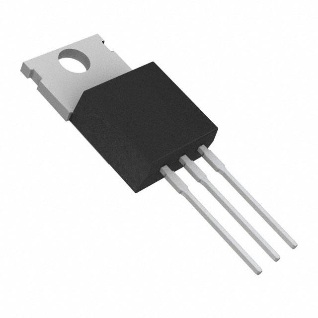
TO−220−3
T SUFFIX
CASE 221AB
PIN CONNECTIONS
Pin 1. Input
2. Ground
3. Output
Heatsink surface
connected to Pin 2
Output
MARKING
DIAGRAM
CO**
78xxT
AWLYWWG
A common ground is required between the input and
the output voltages. The input voltage must remain
typically 2.0 V above the output voltage even during the
low point on the input ripple voltage.
XX These two digits of the type number indicate
nominal voltage.
* Cin is required if regulator is located an appreciable
distance from power supply filter.
xx
A
WL, L
Y
WW
G
= 05, 08, 12 or 15
= Assembly Location
= Wafer Lot
= Year
= Work Week
= Pb−Free Device
ORDERING INFORMATION
See detailed ordering and shipping information in the package
dimensions section on page 11 of this data sheet.
** CO is not needed for stability; however,
it does improve transient response. Values of less
than 0.1 mF could cause instability.
Figure 1. Application Schematic
© Semiconductor Components Industries, LLC, 2010
June, 2010 − Rev. 1
1
Publication Order Number:
NCP7800/D
�NCP7800
Figure 2. Simplified Block Diagram
Table 1. PIN FUNCTION DESCRIPTION
Pin No.
Pin Name
Description
1
Vin
2
GND
Power Supply Ground; Device Substrate.
3
Vout
Regulated Output Voltage.
Positive Power Supply Input.
http://onsemi.com
2
�NCP7800
Table 2. ABSOLUTE MAXIMUM RATINGS (Note 1)
Rating
Input Voltage Range
Symbol
Value
Unit
Vin
−0.3 to 35
V
PD
Internally Limited
W
TJ(max)
150
°C
(for Vout: 5.0 − 15 V)
Power Dissipation
Maximum Junction Temperature
Storage Temperature Range
ESD Capability, Human Body Model (Note 2)
NCP7805, NCP7808
NCP7812, NCP7815
ESD Capability, Machine Model (Note 2)
Tstg
−65 to +150
°C
ESDHBM
4
3
kV
ESDMM
400
V
Stresses exceeding Maximum Ratings may damage the device. Maximum Ratings are stress ratings only. Functional operation above the
Recommended Operating Conditions is not implied. Extended exposure to stresses above the Recommended Operating Conditions may affect
device reliability.
1. Refer to ELECTRICAL CHARACTERISTICS and APPLICATION INFORMATION for Safe Operating Area.
2. This device series incorporates ESD protection and is tested by the following methods:
ESD Human Body Model tested per EIA/JESD22−A114
ESD Machine Model tested per EIA/JESD22−A115
Latchup Current Maximum Rating: ≤150 mA per JEDEC standard: JESD78
Table 3. THERMAL CHARACTERISTICS
Rating
Symbol
Value
RqJC
RqJA
7.5
65
Thermal Characteristics, TO−220−3 (Note 3)
Thermal Resistance, Junction−to−Case
Thermal Resistance, Junction−to−Air (Note 4)
Unit
°C/W
3. Refer to ELECTRICAL CHARACTERISTICS and APPLICATION INFORMATION for Safe Operating Area.
4. Value based on thermal measurement in a test socket.
Table 4. OPERATING RANGES (Note 5)
Rating
Input Voltage (Note 6)
Symbol
Min
Max
Unit
Vin
7.0
35
V
TJ
0
125
°C
(for Vout: 5.0 − 15 V)
Junction Temperature
5. Refer to ELECTRICAL CHARACTERISTICS and APPLICATION INFORMATION for Safe Operating Area.
6. Minimum Vin = 7.0 V or (Vout + VDO), whichever is higher.
http://onsemi.com
3
�NCP7800
Table 5. ELECTRICAL CHARACTERISTICS (Vin = 10 V, IO = 500 mA, TJ = 0°C to 125°C, unless otherwise noted) (Note 7)
NCP7805
Symbol
Min
Typ
Max
Unit
Output Voltage (TJ = 25°C)
VO
4.8
5.0
5.2
Vdc
Output Voltage (5.0 mA ≤ IO ≤ 1.0 A, PD ≤ 15 W)
7.0 Vdc ≤ Vin ≤ 20 Vdc
VO
4.75
5.0
5.25
−
−
1.1
0.6
100
50
−
−
1.5
2.9
50
100
−
3.0
8
−
−
0.28
0.07
1.3
0.5
Characteristic
Line Regulation (TJ = 25°C)
7.5 Vdc ≤ Vin ≤ 20 Vdc
8.0 Vdc ≤ Vin ≤ 12 Vdc
Regline
Load Regulation (TJ = 25°C)
5.0 mA ≤ IO ≤ 1.0 A
5.0 mA ≤ IO ≤ 1.5 A
Regload
Quiescent Current (TJ = 25°C)
IB
Vdc
mV
mV
mA
Quiescent Current Change
7.0 Vdc ≤ Vin ≤ 25 Vdc
5.0 mA ≤ IO ≤ 1.0 A
DIB
Ripple Rejection (Note 8)
8.0 Vdc ≤ Vin ≤ 18 Vdc, f = 120 Hz
RR
62
75
−
VI − VO
−
2.0
−
Vdc
Vn
−
6.8
−
mV/VO
Output Resistance f = 1.0 kHz (Note 8)
rO
−
2.2
−
mW
Short Circuit Current Limit (TJ = 25°C) (Note 8)
Vin = 35 Vdc
ISC
−
0.3
−
A
Peak Output Current (TJ = 25°C) (Note 8)
Imax
−
2.4
−
A
TCVO
−
0.13
−
mV/°C
Dropout Voltage (IO = 1.0 A, TJ = 25°C) (Note 8)
Output Noise Voltage (TJ = 25°C) (Note 8)
10 Hz ≤ f ≤ 100 kHz
Average Temperature Coefficient of Output Voltage (Note 8)
mA
dB
7. Performance guaranteed over the indicated operating temperature range by design and/or characterization, production tested at
TJ = TA = 25°C. Low duty cycle pulse techniques are used during testing to maintain the junction temperature as close to ambient as possible.
8. Value based on design and/or characterization.
http://onsemi.com
4
�NCP7800
Table 6. ELECTRICAL CHARACTERISTICS (Vin = 14 V, IO = 500 mA, TJ = 0°C to 125°C, unless otherwise noted) (Note 9)
NCP7808
Symbol
Min
Typ
Max
Unit
Output Voltage (TJ = 25°C)
VO
7.68
8.0
8.32
Vdc
Output Voltage (5.0 mA ≤ IO ≤ 1.0 A, PD ≤ 15 W)
10.5 Vdc ≤ Vin ≤ 23 Vdc
VO
7.60
8.0
8.40
−
−
1.8
1.0
160
80
−
3.7
160
−
3.0
8.0
−
−
−
−
1.0
0.5
Characteristic
Line Regulation (TJ = 25°C)
10.5 Vdc ≤ Vin ≤ 25 Vdc
11.0 Vdc ≤ Vin ≤ 17 Vdc
Regline
Load Regulation (TJ = 25°C)
5.0 mA ≤ IO ≤ 1.5 A
Regload
Quiescent Current (TJ = 25°C)
IB
Vdc
mV
mV
mA
Quiescent Current Change
10.5 Vdc ≤ Vin ≤ 25 Vdc
5.0 mA ≤ IO ≤ 1.0 A
DIB
Ripple Rejection (Note 10)
11.5 Vdc ≤ Vin ≤ 21.5 Vdc, f = 120 Hz
RR
56
72
−
dB
VI − VO
−
2.0
−
Vdc
Output Noise Voltage (TJ = 25°C) (Note 10)
10 Hz ≤ f ≤ 100 kHz
Vn
−
6.8
−
mV/VO
Output Resistance f = 1.0 kHz (Note 10)
rO
−
2.7
−
mW
Short Circuit Current Limit (TJ = 25°C) (Note 10)
Vin = 35 Vdc
ISC
−
0.3
−
A
Imax
−
2.4
−
A
TCVO
−
0.24
−
mV/°C
Dropout Voltage (IO = 1.0 A, TJ = 25°C) (Note 10)
Peak Output Current (TJ = 25°C) (Note 10)
Average Temperature Coefficient of Output Voltage (Note 10)
mA
9. Performance guaranteed over the indicated operating temperature range by design and/or characterization, production tested at
TJ = TA = 25°C. Low duty cycle pulse techniques are used during testing to maintain the junction temperature as close to ambient as possible.
10. Value based on design and/or characterization.
http://onsemi.com
5
�NCP7800
Table 7. ELECTRICAL CHARACTERISTICS (Vin = 19 V, IO = 500 mA, TJ = 0°C to 125°C, unless otherwise noted) (Note 11)
NCP7812
Symbol
Min
Typ
Max
Unit
Output Voltage (TJ = 25°C)
VO
11.52
12
12.48
Vdc
Output Voltage (5.0 mA ≤ IO ≤ 1.0 A, PD ≤ 15 W)
14.5 Vdc ≤ Vin ≤ 27 Vdc
VO
11.40
12
12.60
−
−
2.7
1.4
240
120
−
5.5
240
−
3.0
8.0
−
−
−
−
1.0
0.5
Characteristic
Line Regulation (TJ = 25°C)
14.5 Vdc ≤ Vin ≤ 30 Vdc
16 Vdc ≤ Vin ≤ 22 Vdc
Regline
Load Regulation (TJ = 25°C)
5.0 mA ≤ IO ≤ 1.5 A
Regload
Quiescent Current (TJ = 25°C)
IB
Vdc
mV
mV
mA
Quiescent Current Change
14.5 Vdc ≤ Vin ≤ 30 Vdc
5.0 mA ≤ IO ≤ 1.0 A
DIB
Ripple Rejection (Note 12)
15 Vdc ≤ Vin ≤ 25 Vdc, f = 120 Hz
RR
55
71
−
dB
VI − VO
−
2.0
−
Vdc
Output Noise Voltage (TJ = 25°C) (Note 12)
10 Hz ≤ f ≤ 100 kHz
Vn
−
6.8
−
mV/VO
Output Resistance f = 1.0 kHz (Note 12)
rO
−
3.6
−
mW
Short Circuit Current Limit (TJ = 25°C) (Note 12)
Vin = 35 Vdc
ISC
−
0.3
−
A
Imax
−
2.4
−
A
TCVO
−
0.47
−
mV/°C
Dropout Voltage (IO = 1.0 A, TJ = 25°C) (Note 12)
Peak Output Current (TJ = 25°C) (Note 12)
Average Temperature Coefficient of Output Voltage (Note 12)
mA
11. Performance guaranteed over the indicated operating temperature range by design and/or characterization, production tested at
TJ = TA = 25°C. Low duty cycle pulse techniques are used during testing to maintain the junction temperature as close to ambient as possible.
12. Value based on design and/or characterization.
http://onsemi.com
6
�NCP7800
Table 8. ELECTRICAL CHARACTERISTICS (Vin = 23 V, IO = 500 mA, TJ = 0°C to 125°C, unless otherwise noted) (Note 13)
NCP7815
Symbol
Min
Typ
Max
Unit
Output Voltage (TJ = 25°C)
VO
14.40
15
15.60
Vdc
Output Voltage (5.0 mA ≤ IO ≤ 1.0 A, PD ≤ 15 W)
17.5 Vdc ≤ Vin ≤ 30 Vdc
VO
14.25
15
15.75
−
−
3.3
1.8
300
150
−
6.9
300
−
3.0
8.0
−
−
−
−
1.0
0.5
Characteristic
Line Regulation (TJ = 25°C)
17.9 Vdc ≤ Vin ≤ 30 Vdc
20 Vdc ≤ Vin ≤ 26 Vdc
Regline
Load Regulation (TJ = 25°C)
5.0 mA ≤ IO ≤ 1.5 A
Regload
Quiescent Current (TJ = 25°C)
IB
Vdc
mV
mV
mA
Quiescent Current Change
17.5 Vdc ≤ Vin ≤ 30 Vdc
5.0 mA ≤ IO ≤ 1.0 A
DIB
Ripple Rejection (Note 14)
18.5 Vdc ≤ Vin ≤ 28.5 Vdc, f = 120 Hz
RR
54
70
−
dB
VI − VO
−
2.0
−
Vdc
Output Noise Voltage (TJ = 25°C) (Note 14)
10 Hz ≤ f ≤ 100 kHz
Vn
−
6.8
−
mV/VO
Output Resistance f = 1.0 kHz (Note 14)
rO
−
4.7
−
mW
Short Circuit Current Limit (TJ = 25°C) (Note 14)
Vin = 35 Vdc
ISC
−
0.3
−
A
Imax
−
2.4
−
A
TCVO
−
0.42
−
mV/°C
Dropout Voltage (IO = 1.0 A, TJ = 25°C) (Note 14)
Peak Output Current (TJ = 25°C) (Note 14)
Average Temperature Coefficient of Output Voltage (Note 14)
mA
13. Performance guaranteed over the indicated operating temperature range by design and/or characterization, production tested at
TJ = TA = 25°C. Low duty cycle pulse techniques are used during testing to maintain the junction temperature as close to ambient as possible.
14. Value based on design and/or characterization.
http://onsemi.com
7
�NCP7800
TYPICAL CHARACTERISTICS
90
2.5
RR, RIPPLE REJECTION (dB)
IO, OUTPUT CURRENT (A)
3.0
TJ = 0°C
2.0
TJ = 25°C
1.5
TJ = 125°C
1.0
0.5
0
0
5
10
15
20
25
35
30
6
8
10
12
14
16
18
20
22
Figure 4. Ripple Rejection as a Function of
Output Voltage
24
5.10
VO, OUTPUT VOLTAGE (V)
RR, RIPPLE REJECTION (dB)
4
Figure 3. Peak Output Current as a Function
of Input/Output Differential Voltage (NCP7805)
60
Vin = 8.0 V to 18 V
IO = 500 mA
TA = 25°C
50
40
0.01
0.1
1
Vin = 20 V
IO = 5.0 mA
5.05
5.00
4.95
4.90
4.85
4.80
−60
10
−20
60
20
100
140
f, FREQUENCY (kHz)
TJ, JUNCTION TEMPERATURE (°C)
Figure 5. Ripple Rejection as a Function of
Frequency (NCP7805)
Figure 6. Output Voltage as a Function of
Junction Temperature (NCP7805)
10
180
6
IB, QUIESCENT CURRENT (mA)
ZO, OUTPUT IMPEDANCE (mW)
PART #� � Vin
NCP7805�= 10 V
NCP7808�= 14 V
NCP7812�= 19 V
NCP7815�= 23 V
60
VO, OUTPUT VOLTAGE (V)
70
1
0.1
70
Vin − Vout, INPUT/OUTPUT VOLTAGE DIFFERENTIAL (V)
80
30
80
50
40
f = 120 Hz
IO = 20 mA
DVin = 1.0 V(RMS)
f = 120 Hz
IO = 500 mA
CL = 0 mF
4
6
8
10
12
14
16
18
20
22
Vin = 10 V
VO = 5.0 V
IL = 20 mA
5
4
3
2
1
0
−50
24
−25
0
25
50
75
100
125
VO, OUTPUT VOLTAGE (V)
TJ, JUNCTION TEMPERATURE (°C)
Figure 7. Output Impedance as a Function of
Output Voltage
Figure 8. Quiescent Current as a Function of
Temperature (NCP7805)
http://onsemi.com
8
�NCP7800
APPLICATIONS INFORMATION
Design Considerations
input bypass capacitor should be selected to provide good
high−frequency characteristics to insure stable operation
under all load conditions. A 0.33 mF or larger tantalum,
mylar, or other capacitor having low internal impedance at
high frequencies should be chosen. The bypass capacitor
should be mounted with the shortest possible leads directly
across the regulators input terminals. Normally good
construction techniques should be used to minimize ground
loops and lead resistance drops since the regulator has no
external sense lead.
The NCP7800 Series of fixed voltage regulators are
designed with Thermal Overload Protection that shuts down
the circuit when subjected to an excessive power overload
condition, Internal Short Circuit Protection that limits the
maximum current the circuit will pass, and Output Transistor
Safe−Area Compensation that reduces the output short circuit
current as the voltage across the pass transistor is increased.
In many low current applications, compensation
capacitors are not required. However, it is recommended
that the regulator input be bypassed with a capacitor if the
regulator is connected to the power supply filter with long
wire lengths, or if the output load capacitance is large. An
NCP7805
Input
0.33 mF
R
IO
Constant
Current to
Grounded
Load
Output
NCP7805
Input
0.33 mF
The NCP7800 regulators can also be used as a current source when
connected as above. In order to minimize dissipation the NCP7805 is
chosen in this application. Resistor R determines the current as follows:
0.1 mF
+
1.0 k
5.0�V
I +
)I
B
O
R
10 k
MC34072V
VO = 7.0 V to 20 V
VIN ≥ VO + 2.0 V
IB ^ 3.2 mA over line and load changes.
For example, a 1.0 A current source would require R to be a 5.0 W,
10 W resistor and the output voltage compliance would be the input
voltage less 7.0 V.
The addition of an operational amplifier allows adjustment to higher or
intermediate values while retaining regulation characteristics. The
minimum voltage obtainable with this arrangement is 2.0 V greater than the
regulator voltage.
Figure 9. Current Regulator
Figure 10. Adjustable Output Regulator
RSource
MJ2955 or Equiv.
Input
Input
0.33 mF
R
RSC
RSource
NCP78XX
0.33 mF
2N6049
or Equiv.
Output
R
≥ 10 mF
1.0 mF
MJ2955
or Equiv.
1.0 mF
≥ 10 mF
NCP78XX
1.0 mF
Output
XX = 2 digits of type number indicating voltage.
XX = 2 digits of type number indicating voltage.
The NCP7800 series can be current boosted with a PNP transistor. The
MJ2955 provides current to 5.0 A. Resistor R in conjunction with the VBE
of the PNP determines when the pass transistor begins conducting; this
circuit is not short circuit proof. Input/output differential voltage minimum is
increased by VBE of the pass transistor.
The circuit of Figure 11 can be modified to provide supply protection
against short circuits by adding a short circuit sense resistor, RSC, and an
additional PNP transistor. The current sensing PNP must be able to handle
the short circuit current of the three-terminal regulator. Therefore, a
four-ampere plastic power transistor is specified.
Figure 11. Current Boost Regulator
Figure 12. Short Circuit Protection
http://onsemi.com
9
�NCP7800
2.5
20
PD , POWER DISSIPATION (W)
Vin - Vout , INPUT-OUTPUT VOLTAGE
DIFFERENTIAL (V)
qHS = 0°C/W
16
qHS = 5°C/W
12
qHS = 15°C/W
8.0
4.0
0
-50
qJC = 7.5°C/W
qJA = 65°C/W
TJ(max) = 150°C
No Heatsink
-25
0
25
50
75
100
125
IO = 500 mA
IO = 200 mA
IO = 20 mA
1.5
IO = 0 mA
1.0
DVO = 2% of VO
0.5
0
-75
150
IO = 1.0 A
2.0
-50
-25
0
25
50
75
100
125
TA, AMBIENT TEMPERATURE (°C)
TJ, JUNCTION TEMPERATURE (°C)
Figure 13. Worst Case Power Dissipation vs.
Ambient Temperature (TO−220)
Figure 14. Input Output Differential as a Function
of Junction Temperature
Protection Diode
several milliseconds. In this case a damage may occur to the
regulator.
To protect the regulator the external bypass diode
connected between output and input is recommended. The
protection diode should be rated for sufficient peak current.
The NCP7800 Series has internal low impedance (about
1 W) diode path that normally does not require protection
when used in the typical regulator applications. The path
connects between output and input and it can withstand a
peak surge current of about 5 A for a reasonable time
(several milliseconds). Normal cycling of Vin cannot
generate a current surge of this magnitude for too long time
since output capacitor discharges from output to input and
follows input voltage therefore the magnitude of reverse
current is not so high. However, when Vin is shorted or
crowbarred to ground and output cap is too large and
moreover if higher voltage option is used then the peak of
reverse current is much higher than 5 A and lasts more than
Protection Diode
Input
Cin
NCP78XX
Output
Cout
Figure 15. Protection Diode Placement
http://onsemi.com
10
�NCP7800
DEFINITIONS
Quiescent Current − That part of the input current that is
not delivered to the load.
Output Noise Voltage − The rms ac voltage at the output,
with constant load and no input ripple, measured over a
specified frequency range.
Long Term Stability − Output voltage stability under
accelerated life test conditions with the maximum rated
voltage listed in the devices’ electrical characteristics and
maximum power dissipation.
Line Regulation − The change in output voltage for a
change in the input voltage. The measurement is made under
conditions of low dissipation or by using pulse techniques
such that the average chip temperature is not significantly
affected.
Load Regulation − The change in output voltage for a
change in load current at constant chip temperature.
Maximum Power Dissipation − The maximum total
device dissipation for which the regulator will operate
within specifications.
ORDERING INFORMATION
Nominal Voltage
Operating
Temperature Range
NCP7805TG
5.0 V
NCP7808TG
Device
Package
Shipping
TJ = 0°C to +125°C
TO−220
(Pb−Free)
50 Units / Rail
8.0 V
TJ = 0°C to +125°C
TO−220
(Pb−Free)
50 Units / Rail
NCP7812TG
12 V
TJ = 0°C to +125°C
TO−220
(Pb−Free)
50 Units / Rail
NCP7815TG
15 V
TJ = 0°C to +125°C
TO−220
(Pb−Free)
50 Units / Rail
http://onsemi.com
11
�MECHANICAL CASE OUTLINE
PACKAGE DIMENSIONS
TO−220, SINGLE GAUGE
CASE 221AB−01
ISSUE A
−T−
B
F
T
SCALE 1:1
SEATING
PLANE
C
S
DATE 16 NOV 2010
NOTES:
1. DIMENSIONING AND TOLERANCING PER ANSI Y14.5M, 1982.
2. CONTROLLING DIMENSION: INCHES.
3. DIMENSION Z DEFINES A ZONE WHERE ALL BODY AND
LEAD IRREGULARITIES ARE ALLOWED.
4. PRODUCT SHIPPED PRIOR TO 2008 HAD DIMENSIONS
S = 0.045 - 0.055 INCHES (1.143 - 1.397 MM)
4
DIM
A
B
C
D
F
G
H
J
K
L
N
Q
R
S
T
U
V
Z
A
Q
U
1 2 3
H
K
Z
L
R
V
J
G
D
N
INCHES
MIN
MAX
0.570
0.620
0.380
0.405
0.160
0.190
0.025
0.035
0.142
0.147
0.095
0.105
0.110
0.155
0.018
0.025
0.500
0.562
0.045
0.060
0.190
0.210
0.100
0.120
0.080
0.110
0.020
0.024
0.235
0.255
0.000
0.050
0.045
----0.080
MILLIMETERS
MIN
MAX
14.48
15.75
9.66
10.28
4.07
4.82
0.64
0.88
3.61
3.73
2.42
2.66
2.80
3.93
0.46
0.64
12.70
14.27
1.15
1.52
4.83
5.33
2.54
3.04
2.04
2.79
0.508
0.61
5.97
6.47
0.00
1.27
1.15
----2.04
STYLE 1:
PIN 1.
2.
3.
4.
BASE
COLLECTOR
EMITTER
COLLECTOR
STYLE 2:
PIN 1.
2.
3.
4.
BASE
EMITTER
COLLECTOR
EMITTER
STYLE 3:
PIN 1.
2.
3.
4.
CATHODE
ANODE
GATE
ANODE
STYLE 4:
PIN 1.
2.
3.
4.
MAIN TERMINAL 1
MAIN TERMINAL 2
GATE
MAIN TERMINAL 2
STYLE 5:
PIN 1.
2.
3.
4.
GATE
DRAIN
SOURCE
DRAIN
STYLE 6:
PIN 1.
2.
3.
4.
ANODE
CATHODE
ANODE
CATHODE
STYLE 7:
PIN 1.
2.
3.
4.
CATHODE
ANODE
CATHODE
ANODE
STYLE 8:
PIN 1.
2.
3.
4.
CATHODE
ANODE
EXTERNAL TRIP/DELAY
ANODE
STYLE 9:
PIN 1.
2.
3.
4.
GATE
COLLECTOR
EMITTER
COLLECTOR
STYLE 10:
PIN 1.
2.
3.
4.
GATE
SOURCE
DRAIN
SOURCE
STYLE 11:
PIN 1.
2.
3.
4.
DRAIN
SOURCE
GATE
SOURCE
DOCUMENT NUMBER:
DESCRIPTION:
98AON23085D
TO−220, SINGLE GAUGE
Electronic versions are uncontrolled except when accessed directly from the Document Repository.
Printed versions are uncontrolled except when stamped “CONTROLLED COPY” in red.
PAGE 1 OF 1
ON Semiconductor and
are trademarks of Semiconductor Components Industries, LLC dba ON Semiconductor or its subsidiaries in the United States and/or other countries.
ON Semiconductor reserves the right to make changes without further notice to any products herein. ON Semiconductor makes no warranty, representation or guarantee regarding
the suitability of its products for any particular purpose, nor does ON Semiconductor assume any liability arising out of the application or use of any product or circuit, and specifically
disclaims any and all liability, including without limitation special, consequential or incidental damages. ON Semiconductor does not convey any license under its patent rights nor the
rights of others.
© Semiconductor Components Industries, LLC, 2019
www.onsemi.com
�onsemi,
, and other names, marks, and brands are registered and/or common law trademarks of Semiconductor Components Industries, LLC dba “onsemi” or its affiliates
and/or subsidiaries in the United States and/or other countries. onsemi owns the rights to a number of patents, trademarks, copyrights, trade secrets, and other intellectual property.
A listing of onsemi’s product/patent coverage may be accessed at www.onsemi.com/site/pdf/Patent−Marking.pdf. onsemi reserves the right to make changes at any time to any
products or information herein, without notice. The information herein is provided “as−is” and onsemi makes no warranty, representation or guarantee regarding the accuracy of the
information, product features, availability, functionality, or suitability of its products for any particular purpose, nor does onsemi assume any liability arising out of the application or use
of any product or circuit, and specifically disclaims any and all liability, including without limitation special, consequential or incidental damages. Buyer is responsible for its products
and applications using onsemi products, including compliance with all laws, regulations and safety requirements or standards, regardless of any support or applications information
provided by onsemi. “Typical” parameters which may be provided in onsemi data sheets and/or specifications can and do vary in different applications and actual performance may
vary over time. All operating parameters, including “Typicals” must be validated for each customer application by customer’s technical experts. onsemi does not convey any license
under any of its intellectual property rights nor the rights of others. onsemi products are not designed, intended, or authorized for use as a critical component in life support systems
or any FDA Class 3 medical devices or medical devices with a same or similar classification in a foreign jurisdiction or any devices intended for implantation in the human body. Should
Buyer purchase or use onsemi products for any such unintended or unauthorized application, Buyer shall indemnify and hold onsemi and its officers, employees, subsidiaries, affiliates,
and distributors harmless against all claims, costs, damages, and expenses, and reasonable attorney fees arising out of, directly or indirectly, any claim of personal injury or death
associated with such unintended or unauthorized use, even if such claim alleges that onsemi was negligent regarding the design or manufacture of the part. onsemi is an Equal
Opportunity/Affirmative Action Employer. This literature is subject to all applicable copyright laws and is not for resale in any manner.
PUBLICATION ORDERING INFORMATION
LITERATURE FULFILLMENT:
Email Requests to: orderlit@onsemi.com
onsemi Website: www.onsemi.com
◊
TECHNICAL SUPPORT
North American Technical Support:
Voice Mail: 1 800−282−9855 Toll Free USA/Canada
Phone: 011 421 33 790 2910
Europe, Middle East and Africa Technical Support:
Phone: 00421 33 790 2910
For additional information, please contact your local Sales Representative
�