NCP786A
Linear Regulator - Wide
Input Voltage Range,
Ultra-Low Iq, High PSRR,
Adjustable Output Voltage
www.onsemi.com
10�mA
The NCP786A is high−performance linear regulator, offering a very
wide operating input voltage range of up to 450 V DC, with an output
current of up to 10 mA. Ideal for high input voltage applications such
as industrial and home metering, home appliances. The NCP786A
family offers ±3% initial accuracy, extremely high−power supply
rejection ratio and ultra−low quiescent current. The NCP786A family
is optimized for high−voltage line and load transients, making them
ideal for harsh environment applications. The output voltage can be set
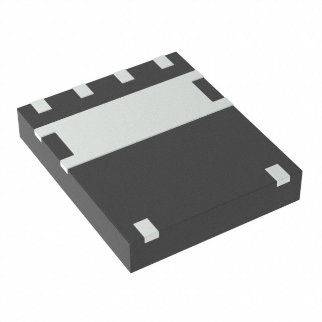
by resistor divider in range from 1.27 V up to 15 V. DFN6 5x6 Pb−free
package with high allowable power dissipation keep small footprint at
space sensitive applications.
Features
• Wide Input Voltage Range:
•
•
•
•
•
•
•
•
DC: Up to 450 V
AC: 85 V to 260 V (half−wave rectifier and 4.7 mF capacitor)
10 mA Guaranteed Output Current
Ultra Low Quiescent Current: Typ. 10 mA (VOUT ≤ 15 V)
±5% Accuracy Over Full Load, Line and Temperature Variations
Ultra−high PSRR: 70 dB at 60 Hz, 90 dB at 100 kHz
Stable with Ceramic Output Capacitor 2.2 mF MLCC
Thermal Shutdown and Current Limit Protection
Available in DFN6 5x6 Package
This is a Pb−Free Device
MARKING
DIAGRAM
DFN6 5x6
ST SUFFIX
CASE 506DV
786A
XXX
ALLYYWWG
G
(Top View)
786A = Specific Device Marking
XXX = Voltage Version
(see page 7)
A
= Assembly Location
LL = Wafer Lot
YY = Year
WW = Work Week
G
= Pb−Free Package
(Note: Microdot may be in either location)
Typical Applications
• Industrial Applications, Home Appliances
• Home Metering / Network Application
• Off−line Power Supplies
© Semiconductor Components Industries, LLC, 2017
Octoeber, 2019 − Rev. 3
ORDERING INFORMATION
See detailed ordering and shipping information in the package
dimensions section on page 7 of this data sheet.
1
Publication Order Number:
NCP786A/D
�NCP786A
3
Vin = (55 – 450) V
VIN
NC
1
5
VIN
VOUT
NCP786
DFN6 5x6
2
6
NC
ADJ
VOUT = (1.275 – 15.0) V / 10mA
VOUT
R1
GND EP
CIN
4
4.7 mF
COUT
EP
2.2 mF
R2
GND
GND
Figure 1. Typical Applications
VIN
Thermal
Shutdown
Current
Limit
VREF
1.27V
+
−
+
−
VOUT
GND
ADJ
Figure 2. Simplified Internal Block Diagram
Table 1. PIN FUNCTION DESCRIPTION
Pin No.
Pin Name
1
VIN
Description
Supply Voltage Input. Connect 4.7 mF capacitor from VIN to GND.
2
NC
Not connected.
3
NC
Not connected.
4
GND
Ground connection.
5
VOUT
Regulator Output. Connect 2.2 mF or higher MLCC capacitor from VOUT to GND.
6
ADJ
ADJ pin for output voltage setting via resistors divider.
EP
EP
EP should be connected to GND potential.
Table 2. ABSOLUTE MAXIMUM RATINGS
Rating
Input Voltage (Note 1)
Output Voltage
Maximum Junction Temperature
www.onsemi.com
2
Symbol
Value
Unit
VIN
−0.3 to 700
V
VOUT
−0.3 to 18
V
TJ(MAX)
125
°C
�NCP786A
Table 2. ABSOLUTE MAXIMUM RATINGS
Storage Temperature
TSTG
−55 to 150
°C
ESD Capability, Human Body Model (All pins except HV pin no.1) (Note 2)
ESDHBM
2000
V
ESD Capability, Machine Model (Note 2)
ESDMM
200
V
Stresses exceeding those listed in the Maximum Ratings table may damage the device. If any of these limits are exceeded, device functionality
should not be assumed, damage may occur and reliability may be affected.
1. Peak 650 V max 1 ms non repeated for 1 s
2. This device series incorporates ESD protection and is tested by the following methods:
ESD Human Body Model tested per AEC−Q100−002 (EIA/JESD22−A114)
ESD Machine Model tested per AEC−Q100−003 (EIA/JESD22−A115)
Latch−up Current Maximum Rating tested per JEDEC standard: JESD78.
Table 3. THERMAL CHARACTERISTICS
Rating
Thermal Characteristics, DFN6
Thermal Resistance, Junction−to−Air
JEDEC 51.3, One side, 600 sq mm PCB
Symbol
Value
Unit
RqJA
82
°C/W
www.onsemi.com
3
�NCP786A
Table 4. ELECTRICAL CHARACTERISTICS NCP786A Adj. (−40°C ≤ TJ ≤ 85°C; VIN = 340 V; IOUT = 100 mA, CIN = 4.7 mF,
COUT = 10 mF, unless otherwise noted. Typical values are at TJ = +25°C.) (Note 3)
Parameter
Test Conditions
Operating Input Voltage DC
Maximum output voltage
Reference Voltage Accuracy
Symbol
Min
VIN
55
Voutmax
−40°C ≤ TJ ≤ 85°C, Iout = 100 mA,
55 V ≤ Vin ≤ 450 V
Typ
Max
Unit
450
V
15
V
TJ = 25°C, Iout = 100 mA, 55 V ≤ Vin ≤ 450 V
VREF
−3%
1.275
+3%
V
−40°C ≤ TJ ≤ 85°C, Iout = 100 mA,
55 V ≤ Vin ≤ 450 V
VREF
−5%
1.275
+5%
V
Line Regulation
VIN = 55 V to 450 V, Iout = 100 mA
RegLINE
−0.5
0.1
+0.5
%
Load Regulation
IOUT = 100 mA to 10 mA, Vin = 55 V
RegLOAD
−1.0
0.7
+1.0
%
Maximum Output Current
55 V ≤ Vin ≤ 450 V, (Note 4)
IOUT
11
Quiescent Current
IOUT = 0, 55 V ≤ Vin ≤ 450 V
IGND
Ground current
55 V ≤ Vin ≤ 450 V, (Note 4)
0 < IOUT ≤ 10 mA
mA
10
ADJ Pin current
15
mA
25
mA
150
nA
Power Supply Rejection Ratio
Vin = 340 VDC +1 Vpp modulation,
Iout = 100 mA
f = 1 kHz
PSRR
65
dB
Noise
f = 10 kHz to 1 MHz Vin = 340 VDC, Iout = 1 mA,
COUT = 10 mF
VNOISE
150
mVrms
Thermal Shutdown Temperature
(Note 5)
Temperature increasing from TJ = +25°C
TSD
145
°C
Thermal Shutdown Hysteresis
(Note 5)
Temperature falling from TSD
TSDH
−
10
−
°C
Product parametric performance is indicated in the Electrical Characteristics for the listed test conditions, unless otherwise noted. Product
performance may not be indicated by the Electrical Characteristics if operated under different conditions.
3. Performance guaranteed over the indicated operating temperature range by design and/or characterization production tested at TJ = TA =
25°C. Low duty cycle pulse techniques are used during testing to maintain the junction temperature as close to ambient as possible.
4. Respect to Safe Operating Area
5. Guaranteed by design
www.onsemi.com
4
�NCP786A
TYPICAL CHARACTERISTICS
1.279
1.277
1.278
OUTPUT VOLTAGE (V)
1.278
OUTPUT VOLTAGE (V)
1.279
TA = 85°C
TA = 25°C
1.276
TA = 0°C
1.275
NCP786A Adj. VOUT(nom) = 1.275 V
CIN = 4.7 mF, COUT = 10 mF
IOUT = 100 mA
1.274
1.273
1.272
100
150
200
250
300
350
0
20
40
60
80
Figure 3. Output Voltage vs. Input Voltage
Figure 4. Output Voltage vs. Temperature
1.278
1.276
8
7
6
5
1.274
VIN = 55 V
VIN = 75 V
VIN = 100 V
VIN = 150 V
VIN = 200 V
VIN = 250 V
VIN = 300 V
VIN = 350 V
1.272
1.270
1.268
4
50
100
150
200
250
300
350
1.266
450
400
0
1
2
3
NCP786A Adj. TA = 25°C
CIN = 4.7 mF, COUT = 10 mF
VOUT(nom) = 1.275 V
4
5
6
7
8
9
INPUT VOLTAGE (V)
OUTPUT CURRENT (mA)
Figure 5. Quiescent Current vs. Input Voltage
Figure 6. Output Voltage vs. Output Current
25
NOISE DENSITY (mV√Hz)
−20
TEMPERATURE (°C)
9
20
15
10
5
0
VIN = 55 V
VIN = 150 V
VIN = 250 V
VIN = 350 V
VIN = 450 V
1.274
INPUT VOLTAGE (V)
OUTPUT VOLTAGE (V)
QUIESCENT CURRENT (mA)
1.275
1.272
−40
450
400
10
3
1.276
1.273
TA = −40°C
50
1.277
0.01
0.1
1
10
100
1000
FREQUENCY (kHz)
Figure 7. Noise Density vs. Frequency
www.onsemi.com
5
10
�NCP786A
APPLICATION INFORMATION
Vin = (55 – 450) Vdc
NC
IN
OUT
Vout = 1.275 V – 15 V / 10 mA
R1
NCP786A
Cin
Cout
NC GND EP ADJ
Vin = (85 – 265) Vac
NC
IN
Cin
OUT
R2
Vout = 1.275 V – 15 V / 10 mA
R1
NCP786A
Cout
NC GND EP ADJ
Vin = (85 – 265) Vac
NC
IN
Cin
OUT
R2
Vout = 1.275 V – 15 V / 10 mA
NCP786A
NC
GND EP
R1
Cout
ADJ
R2
Figure 8. Typical Application Schematics
Input Decoupling (C1)
Layout Recommendations
A 4.7 mF capacitor either ceramic or electrolytic is
recommended and should be connected close to the input pin
of NCP786A. Higher value 4.7 mF is necessary to keep the
input voltage above the required minimum input voltage at
full load for AC voltage as low as 85 V with half wave
rectifier. The capacitor 2.2 mF or 1 mF could be acceptable
for DC input voltage or AC input voltage 235 V ±20%.
There must be assured minimum Input Voltage more than
55 V at input pin of NCP786A regulator in order to keep
stable desired output voltage with guaranteed parameters.
Please be sure that the VIN and GND lines are sufficiently
wide. When the impedance of these lines is high, there is a
chance to pick up noise or to cause the malfunction of
regulator.
Set external components, especially the output capacitor,
as close as possible to the circuit, and make leads as short as
possible.
Thermal
As power across the NCP786A increases, it might become
necessary to provide some thermal relief. The maximum
power dissipation supported by the device is dependent
upon board design layout and used package. Mounting pad
configuration on the PCB, the board material, and also the
ambient temperature affect the rate of temperature rise for
the part. This is stating that when the NCP786A has good
thermal conductivity through the PCB, the junction
temperature will be relatively low with high power
dissipation applications.
Output Decoupling (C2)
The NCP786A Regulator does not require any specific
Equivalent Series Resistance (ESR). Thus capacitors
exhibiting ESRs ranging from a few mW up to 0.5 W can be
used safely. The minimum decoupling value is 2.2 mF. The
regulator accepts ceramic chip capacitors as well as
tantalum devices or low ESR electrolytic capacitors. Larger
values improve noise rejection and especially load transient
response.
www.onsemi.com
6
�NCP786A
Output Voltage
The output voltage can be set by using a resistor divider
as shown in Figure 1 in range from 1.275 V up to 15 V. The
appropriate resistor divider can be found by solving the
equation below.
V OUT + 1.275
ǒ1 ) R1
Ǔ ) ǒIADJ
R2
R1Ǔ
The recommended current through the resistor divider is
from 1 mA to 3 mA in order to keep negligible ADJ pin
consumption. In this case we can simplify Equation 1 to:
V OUT + 1.275
(eq. 1)
ǒ1 ) R1
Ǔ
R2
(eq. 2)
ORDERING INFORMATION
Part Number
Output Voltage
Marking
Package
Shipping†
NCP786AMNADJTBG
Adjustable
ADJ
DFN6 5x6
(Pb−Free)
1000 / Tape & Reel
†For information on tape and reel specifications, including part orientation and tape sizes, please refer to our Tape and Reel Packaging
Specifications Brochure, BRD8011/D.
www.onsemi.com
7
�MECHANICAL CASE OUTLINE
PACKAGE DIMENSIONS
DFN6 5x6, 1.27P
CASE 506DV
ISSUE O
DATE 12 OCT 2016
SCALE 2:1
D
B
A
L
ALTERNATE A−1
PIN ONE
REFERENCE
ALTERNATE TERMINAL
CONSTRUCTIONS
ÉÉÉ
ÉÉÉ
ÇÇÇ
TOP VIEW
0.08 C
A
A3
e2
1
2
C
6X
L
ÉÉÉ
ÉÉÉ
ÇÇÇ
A3
A1
ALTERNATE B−2
DETAIL B
SEATING
PLANE
ALTERNATE
CONSTRUCTIONS
DIM
A
A1
A3
b
D
D2
E
E2
e
e2
K
L
XXXXXXXX
XXXXXXXX
ALLYYWWG
G
5.30
4.41
E2
6
e
6X
0.60
6
3
1.27 PITCH
3
D2
BOTTOM VIEW
1.95
6.30
0.20
6X
0.75
PACKAGE
OUTLINE
1
3.81
PITCH
2
MILLIMETERS
MIN
NOM
MAX
0.80
0.90
1.00
−−−
−−−
0.05
0.20 REF
0.30
0.40
0.50
4.90
5.00
5.10
4.10
4.20
4.30
5.90
6.10
6.00
1.75
1.85
1.95
1.27 BSC
3.81 BSC
0.25
−−−
−−−
0.45
0.55
0.65
GENERIC
MARKING DIAGRAM*
RECOMMENDED
SOLDERING FOOTPRINT*
DETAIL A
K
MOLD CMPD
ALTERNATE B−1
A1
SIDE VIEW
NOTE 4
10X b
0.10 C A B
0.05 C NOTE 3
EXPOSED Cu
DETAIL A
0.10 C
ALTERNATE A−2
DETAIL A
E
ÉÉ
ÉÉ
NOTES:
1. DIMENSIONING AND TOLERANCING PER
ASME Y14.5M, 1994.
2. CONTROLLING DIMENSION: MILLIMETER.
3. DIMENSION b APPLIES TO PLATED
TERMINAL AND IS MEASURED BETWEEN
0.20 AND 0.25 MM FROM THE TERMINAL TIP.
4. COPLANARITY APPLIES TO THE EXPOSED
PAD AS WELL AS THE TERMINALS.
5. FOR DEVICE OPN CONTAINING W OPTION,
DETAIL B ALTERNATE B−1 AND DETAIL A
ALTERNATE A−1 CONSTRUCTIONS ARE
NOT APPLICABLE.
L
A
= Assembly Location
LL = Wafer Lot
YY = Year
WW = Work Week
G
= Pb−Free Package
(Note: Microdot may be in either location)
*This information is generic. Please refer to
device data sheet for actual part marking.
Pb−Free indicator, “G” or microdot “ G”,
may or may not be present.
DIMENSIONS: MILLIMETERS
*For additional information on our Pb−Free strategy and soldering
details, please download the ON Semiconductor Soldering and
Mounting Techniques Reference Manual, SOLDERRM/D.
DOCUMENT NUMBER:
DESCRIPTION:
98AON16235G
DFN6 5X6, 1.27P
Electronic versions are uncontrolled except when accessed directly from the Document Repository.
Printed versions are uncontrolled except when stamped “CONTROLLED COPY” in red.
PAGE 1 OF 1
ON Semiconductor and
are trademarks of Semiconductor Components Industries, LLC dba ON Semiconductor or its subsidiaries in the United States and/or other countries.
ON Semiconductor reserves the right to make changes without further notice to any products herein. ON Semiconductor makes no warranty, representation or guarantee regarding
the suitability of its products for any particular purpose, nor does ON Semiconductor assume any liability arising out of the application or use of any product or circuit, and specifically
disclaims any and all liability, including without limitation special, consequential or incidental damages. ON Semiconductor does not convey any license under its patent rights nor the
rights of others.
© Semiconductor Components Industries, LLC, 2019
www.onsemi.com
�onsemi,
, and other names, marks, and brands are registered and/or common law trademarks of Semiconductor Components Industries, LLC dba “onsemi” or its affiliates
and/or subsidiaries in the United States and/or other countries. onsemi owns the rights to a number of patents, trademarks, copyrights, trade secrets, and other intellectual property.
A listing of onsemi’s product/patent coverage may be accessed at www.onsemi.com/site/pdf/Patent−Marking.pdf. onsemi reserves the right to make changes at any time to any
products or information herein, without notice. The information herein is provided “as−is” and onsemi makes no warranty, representation or guarantee regarding the accuracy of the
information, product features, availability, functionality, or suitability of its products for any particular purpose, nor does onsemi assume any liability arising out of the application or use
of any product or circuit, and specifically disclaims any and all liability, including without limitation special, consequential or incidental damages. Buyer is responsible for its products
and applications using onsemi products, including compliance with all laws, regulations and safety requirements or standards, regardless of any support or applications information
provided by onsemi. “Typical” parameters which may be provided in onsemi data sheets and/or specifications can and do vary in different applications and actual performance may
vary over time. All operating parameters, including “Typicals” must be validated for each customer application by customer’s technical experts. onsemi does not convey any license
under any of its intellectual property rights nor the rights of others. onsemi products are not designed, intended, or authorized for use as a critical component in life support systems
or any FDA Class 3 medical devices or medical devices with a same or similar classification in a foreign jurisdiction or any devices intended for implantation in the human body. Should
Buyer purchase or use onsemi products for any such unintended or unauthorized application, Buyer shall indemnify and hold onsemi and its officers, employees, subsidiaries, affiliates,
and distributors harmless against all claims, costs, damages, and expenses, and reasonable attorney fees arising out of, directly or indirectly, any claim of personal injury or death
associated with such unintended or unauthorized use, even if such claim alleges that onsemi was negligent regarding the design or manufacture of the part. onsemi is an Equal
Opportunity/Affirmative Action Employer. This literature is subject to all applicable copyright laws and is not for resale in any manner.
PUBLICATION ORDERING INFORMATION
LITERATURE FULFILLMENT:
Email Requests to: orderlit@onsemi.com
onsemi Website: www.onsemi.com
◊
TECHNICAL SUPPORT
North American Technical Support:
Voice Mail: 1 800−282−9855 Toll Free USA/Canada
Phone: 011 421 33 790 2910
Europe, Middle East and Africa Technical Support:
Phone: 00421 33 790 2910
For additional information, please contact your local Sales Representative
�