DATA SHEET
www.onsemi.com
Single Channel 10A High
Speed Low-Side MOSFET
Driver
MARKING
DIAGRAMS
DFN8
MN SUFFIX
CASE 506AA
1
XXMG
G
1
NCP81074A, NCP81074B
The NCP81074 is a single channel, low−side MOSFET driver. It is
capable of providing large peak currents into capacitive loads. This
driver can deliver a 7 A peak current at the Miller plateau region to
help reduce the Miller effect during MOSFETs switching transitions.
It exhibits a split output configuration allowing the user to control the
turn on and turn off slew rates. This part is available in SOIC−8 and
DFN8 2x2 mm packages.
Features
•
•
•
•
•
•
•
•
•
High Current Drive Capability ±10 A
TTL/CMOS Compatible Inputs Independent of Supply Voltage
High Reverse Current Capability (10 A) Peak
4 ns Typical Rise and 4 ns Typical Fall Times with 1.8 nF Load
Fast Propagation Delay Times of 15 ns with Input Falling and 15 ns
with Input Rising
Input Voltage Range from 4.5 V to 20 V
Split Output Configuration
Dual Input Design Offering Drive Flexibility
These Devices are Pb−Free, Halogen Free/BFR Free and are RoHS
Compliant
XX = Specific Device Code
M = Date Code
G
= Pb−Free Device
(Note: Microdot may be in either location)
8
8
1
SOIC−8
CASE 751
1
XXXXXX
AYWW
G
XXXXXX = Specific Device Code
A
= Assembly Location
Y
= Year
WW
= Work Week
G
= Pb−Free Package
ORDERING INFORMATION
See detailed ordering, marking and shipping information on
page 2 of this data sheet.
Applications
•
•
•
•
•
•
•
•
Server Power
Telecommunication, Datacenter Power
Synchronous Rectifier
Switch Mode Power Supply
DC/DC Converter
Power Factor Correction
Motor Drive
Renewable Energy, Solar Inverter
© Semiconductor Components Industries, LLC, 2015
July, 2022 − Rev. 4
1
Publication Order Number:
NCP81074/D
�NCP81074A, NCP81074B
ORDERING INFORMATION
Device
Temperature
Range (5C)
Marking
Input Type
Package Type
Shipping†
NCP81074AMNTBG
−40 to +140
CL
Fixed Digital Threshold
DFN8 2x2
(Pb−Free)
3000 / Tape & Reel
NCP81074BMNTBG
−40 to +140
CM
VDD Based Threshold
DFN8 2x2
(Pb−Free)
3000 / Tape & Reel
NCP81074ADR2G
−40 to +140
NCP81074A
Fixed Digital Threshold
SOIC−8
(Pb−Free)
2500 / Tape & Reel
NCP81074BDR2G
−40 to +140
NCP81074B
VDD Based Threshold
SOIC−8
(Pb−Free)
2500 / Tape & Reel
†For information on tape and reel specifications, including part orientation and tape sizes, please refer to our Tape and Reel Packaging
Specifications Brochure, BRD8011/D.
BLOCK DIAGRAM
Figure 1. NCP81074 Block Diagram
www.onsemi.com
2
�NCP81074A, NCP81074B
PIN DESCRIPTION
Pin No.
Symbol
1
IN+
2
GND
Common ground. This ground should be connected very closely to the source of the power MOSFET.
3
GND
Common ground. This ground should be connected very closely to the source of the power MOSFET.
4
OUTL
Sink pin. Connect to Gate of MOSFET.
5
OUTH
Source Pin. Connect to Gate of MOSFET.
6
VDD
Power Supply Input Pin.
7
VDD
Power supply Input Pin.
IN−
Inverting Input which has logic compatible threshold and hysteresis. If not used, this pin should be
connected to GND. It should not be left unconnected.
8
Description
Non−Inverting Input which has logic compatible threshold and hysteresis. If not used, this pin should be
connected to VDD. It should not be left unconnected.
Figure 2. TYPICAL APPLICATION CIRCUIT
ABSOLUTE MAXIMUM RATINGS
Value
Parameter
Supply Voltage
VDD
Output Current (DC)
Min
Max
Unit
−0.3
24
V
Iout_dc
0.6
A
10
Reverse Current (Pulse
很抱歉,暂时无法提供与“NCP81074AMNTBG”相匹配的价格&库存,您可以联系我们找货
免费人工找货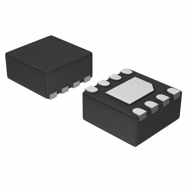


 工商网监
湘ICP备2023018690号
工商网监
湘ICP备2023018690号
