NCP81233
Multi‐Phase Controller with
I2C Interface for DrMOS
The NCP81233, a multi-phase synchronous buck controller with an
I2C interface, provides power management solutions for applications
supported by DrMOS. It supports 1-, 2-, 3-, 4-, or 6-phase operation
and provides differential voltage and current sense, flexible
programming, and comprehensive protections.
www.onsemi.com
Features
•
•
•
•
•
•
•
•
•
•
•
•
•
•
•
•
•
•
•
•
•
•
•
•
•
Selectable 1-, 2-, 3-, 4-, or 6-Phase Operation
Support up to 12-Phase Operation with Phase Doublers
I2C Interface with 8 Programmable Addresses
Vin = 4.5 V ~ 20 V with Input Feedforward
Integrated 5.35 V LDO and 3.3 V LDO
Fsw = 200 k ~ 1.2 MHz
Vout = 0.6 V ~ 5.3 V with 0.25 V~1.52 V DAC (5 mV/step)
Programmable Vboot Voltage 0.6V ~ 1.23V (10mV/step) with
Restore Function
DVID Slew Rate Options (0.125 mV/us, 0.25 mV/us, 0.5 mV/us, 1
mV/us, 2 mV/us, 4 mV/us, 8 mV/us, 16 mV/us)
Programmable External Reference Input
PWM Output Compatible to 3.3 V and 5 V DrMOS
Differential Output Voltage Sense
Differential Current Sense Compatible for both Inductor DCR Sense
and DrMOS Iout Signal
Programmable Load Line
Report of Vout and Iout
Enable with Programmable Input UVLO
DrMOS Power Ready Detection (DRVON)
Externally Programmable Soft Start
Power Saving Interface
Power Good Indicator
Programmable Over Current Protection
Programmable Over/Under Voltage Protection
Hiccup Over Temperature Protection
Thermal Shutdown Protection
This is a Pb-Free Device
Typical Applications
•
•
•
•
January, 2019 − Rev. 1
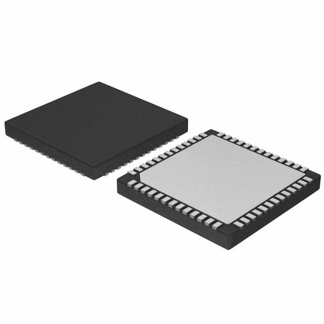
52
GFN52 6x6, O.4P
CASE 485BE
PINOUT
52 PIN, QFN
52
51
50
49
48
47
46
45
44
43
42
37
41
40
1
39
2
38
3
37
4
36
35
5
34
6
GND
53
7
8
33
32
9
31
10
30
11
29
12
28
27
13
14
15
16
17
18
19
20
21
22
23
24
24
25
26
For more details see Figure 1.
MARKING DIAGRAM*
NCP81233
AWLYYWWG
A
WL
YY
WW
G
= Assembly Location
= Wafer Lot
= Year
= Work Week
= Pb-Free Package
*This information is generic. Please refer to
device data sheet for actual part marking.
Pb-Free indicator, “G” or microdot “ G”,
may or may not be present.
ORDERING INFORMATION
Telecom Applications
Server and Storage System
Graphics Card Applications
Multiphase DC-DC Power Management
© Semiconductor Components Industries, LLC, 2017
1
Device
NCP81233MNTXG
Package
Shipping†
QFN52
(Pb-Free)
2500 / Tape & Reel
†For information on tape and reel specifications, including part orientation and tape sizes, please refer
to our Tape and Reel Packaging Specifications
Brochure, BRD8011/D.
1
Publication Order Number:
NCP81233/D
�52
51
50
49
48
47
46
45
44
43
42
41
40
REFIN
VSN
VSP
DIFFOUT
FB
COMP
NC
VDRP
VDFB
CSSUM
VREF
OTP
ILMT
NCP81233
1
IMON
ISP1
39
2
IMAX
ISN1
38
3
VBOOT1
ISN2
37
4
VBOOT2
ISP2
36
5
SS
ISP3
35
6
FSET
ISN3
34
7
CONFIG
ISN4
33
8
MODE1
ISP4
32
9
MODE2
ISP5
31
10
ADDR
ISN5
30
11
SDA
ISN6
29
12
ALERT#
ISP6
28
13
SCL
VB_RST#/PSI
27
PGOOD
DRVON
EN
VIN
VCC5V
VCC3V
PVCC
PWM6
PWM5
PWM4
PWM3
PWM2
PWM1
GND
53
14
15
16
17
18
19
20
21
22
23
24
25
26
Figure 1. Pin Configuration
www.onsemi.com
2
�NCP81233
TABLE 1. PIN DESCRIPTION
Pin
Name
Type
1
IMON
Analog Output
2
IMAX
Analog Input
Current Maximum. A resistor from this pin to ground programs IMAX.
3
VBOOT1
Analog Input
Boot-Up Voltage 1. A resistor from this pin to ground programs boot voltage
4
VBOOT2
Analog Input
Boot-Up Voltage 2. A resistor from this pin to ground programs boot voltage.
5
SS
Analog Input
Soft-Start Slew Rate. A resistor from this pin to ground programs soft-start slew rate.
6
FSET
Analog Input
Frequency Selection. A resistor from this pin to ground programs switching frequency
per phase.
7
CONFIG
Analog Input
Configuration. A resistor from this pin to ground programs configuration of power
stages.
8
MODE1
Analog Input
Mode Programming 1. A resistor from this pin to ground programs configuration of
operation functions.
9
MODE2
Analog Input
Mode Programming 2. A resistor from this pin to ground programs configuration of
operation functions.
10
ADDR
Analog Input
Address. A resistor from this pin to ground programs address of I2C interface.
11
SDA
Logic Bidirectional
12
ALERT#
Logic Output
13
SCL
Logic Input
14
PGOOD
Logic Output
Power GOOD. Open-drain output. Provides a logic high valid power good output
signal, indicating the regulator’s output is in regulation window.
15
DRVON
Analog Input
Driver On. High input voltage means power supply of DrMOS’s driver is ready.
16
EN
Analog Input
Enable. Logic high enables controller while logic low disables controller. Input supply
UVLO can be programmed at this pin.
17
VIN
Power Input
Power Supply Input. Power supply input pin of the device, which is connected to the
integrated 5.35 V LDO and 3.3 V LDO. 4.7 mF or more ceramic capacitors must
bypass this input to power ground. The capacitors should be placed as close as
possible to this pin.
18
VCC5V
Analog Power
Voltage Supply of Controller. Output of integrated 5.35 V LDO and power input pin of
analog circuits. A 4.7 mF ceramic capacitor bypasses this input to GND. This
capacitor should be placed as close as possible to this pin.
19
VCC3V
Analog Power
3.3 V Voltage Supply. Output of integrated 3.3 V LDO. A 4.7 mF ceramic capacitor
bypasses this input to GND. This capacitor should be placed as close as possible to
this pin.
20
PVCC
Analog Power
Voltage Supply of PWM Drivers. Power supply input pin of internal PWM drivers and
digital circuits, which is connected to VCC5 V via a 4.7 Ω resistor. A 1 mF or larger
ceramic capacitor bypasses this input to ground. This capacitor should be placed as
close as possible to this pin.
21
PWM6
Analog Output
PWM 6. PWM output of phase 6.
22
PWM5
Analog Output
PWM 5. PWM output of phase 5.
23
PWM4
Analog Output
PWM 4. PWM output of phase 4.
24
PWM3
Analog Output
PWM 3. PWM output of phase 3.
25
PWM2
Analog Output
PWM 2. PWM output of phase 2.
26
PWM1
Analog Output
PWM 1. PWM output of phase 1.
27
VB_RST# /
PSI
Logic Input
28
ISP6
Analog Input
Description
OUT Current Monitor. Provides output signal representing output current by
connecting a capacitor from this pin to ground.
Serial Data I/O Port. Data port of I2C interface.
ALERT. Open-drain output. Provides a logic low valid alert signal.
Serial Clock. Clock input of I2C interface.
VBOOT Restore. Logic low restores output to boot voltage.
Power Saving Interface. Logic high enables Multi-phase CCM operation, and logic
low enables 1-phase CCM operation.
Pin function is programmed at MODE2 pin.
Current Sense Positive Input 6. Non-inverting input of differential current sense
amplifier of phase 6.
www.onsemi.com
3
�NCP81233
TABLE 1. PIN DESCRIPTION (continued)
Pin
Name
Type
Description
29
ISN6
Analog Input
Current Sense Negative Input 6. Inverting input of differential current sense amplifier
of phase 6.
30
ISN5
Analog Input
Current Sense Negative Input 5. Inverting input of differential current sense amplifier
of phase 5.
31
ISP5
Analog Input
Current Sense Positive Input 5. Non-inverting input of differential current sense
amplifier of phase 5.
32
ISP4
Analog Input
Current Sense Positive Input 4. Non-inverting input of differential current sense
amplifier of phase 4.
33
ISN4
Analog Input
Current Sense Negative Input 4. Inverting input of differential current sense amplifier
of phase 4.
34
ISN3
Analog Input
Current Sense Negative Input 3. Inverting input of differential current sense amplifier
of phase 3.
35
ISP3
Analog Input
Current Sense Positive Input 3. Non-inverting input of differential current sense
amplifier of phase 3.
36
ISP2
Analog Input
Current Sense Positive Input 2. Non-inverting input of differential current sense
amplifier of phase 2.
37
ISN2
Analog Input
Current Sense Negative Input 2. Inverting input of differential current sense amplifier
of phase 2.
38
ISN1
Analog Input
Current Sense Negative Input 1. Inverting input of differential current sense amplifier
of phase 1.
39
ISP1
Analog Input
Current Sense Positive Input 1. Non-inverting input of differential current sense
amplifier of phase 1.
40
ILMT
Analog Input
Limit of Current. Voltage at this pin sets over-current threshold.
41
OTP
Analog Input
Over Temperature Protection. Voltage at this pin sets over-temperature threshold.
42
VREF
Analog Output
Output of Reference. Output of 0.6 V reference. A 10 nF ceramic capacitor bypasses
this input to GND. This capacitor should be placed as close as possible to this pin.
43
CSSUM
Analog Output
Current Sense SUM. Output of current sum amplifier.
44
VDFB
Analog Output
Droop Amplifier Feedback. Inverting input of droop amplifier
45
VDRP
Analog Output
Droop Amplifier Output. Output of droop amplifier.
46
NC
No Connection
47
COMP
Analog Output
48
FB
Analog Input
49
DIFFOUT
Analog Output
Differential Amplifier Output. Output pin of differential voltage sense amplifier.
50
VSP
Analog Input
Voltage Sense Positive Input. Non-inverting input of differential voltage sense
amplifier.
51
VSN
Analog Input
Voltage Sense Negative Input. Inverting input of differential voltage sense amplifier.
52
REFIN
Analog Input
Reference Voltage Input. External reference voltage input.
53
THERM/GND
Analog Ground
Compensation. Output pin of error amplifier.
Feedback. Inverting input of internal error amplifier.
Thermal Pad and Analog Ground. Ground of internal control circuits. Must be
connected to the system ground.
www.onsemi.com
4
�NCP81233
VIN
VIN
PVCC
PWM1
PWM
VCC5V
VIN
VSWH
NCP5339
CGND
3V3
PGND
ISP1
VREF
ISN1
OTP
PWM2
ISP2
ISN2
PWM3
ISP3
ISN3
ILMT
DRVON
EN
PGOOD
VB_RST#
DRVON
PWM4
ISP4
EN
NCP81233 ISN4
PGOOD
PWM5
VB_RST# /
PSI
ISP5
ISN5
CONFIG
MODE1
PWM6
ISP6
ISN6
MODE2
REFIN
VBOOT1
VSN
VBOOT2
VSP
SS
FSET
DIFFOUT
ADDR
SCL
SDA
ALERT#
FB
SCL
COMP
SDA
ALERT#
GND
Figure 2. Typical Application Circuit with Programmed Boot Voltage
www.onsemi.com
5
VOUT
�NCP81233
VIN
PVCC
VIN
PWM1
PWM
VSWH
NCP5339
CGND
PGND
VCC5V
3V3
ISP1
VREF
ISN1
OTP
PWM2
ISP2
ISN2
PWM3
ISP3
ISN3
ILMT
DRVON
EN
PGOOD
PSI
DRVON
PWM4
ISP4
NCP81233 ISN4
PGOOD
PWM5
VB_RST# /
ISP5
PSI
ISN5
CONFIG
EN
MODE1
PWM6
ISP6
ISN6
MODE2
REF
VIN
REFIN
VBOOT1
VSN
VBOOT2
VSP
SS
FSET
ADDR
SCL
SDA
ALERT#
DIFFOUT
FB
SCL
COMP
SDA
ALERT#
GND
Figure 3. Typical Application Circuit with External Reference Input
www.onsemi.com
6
VOUT
�NCP81233
VIN
NCP5339
PWM
VIN
VOUT
VSWH
PGND
PWMA
CSPA
VCCD
PWM1
CSNA
CSNB
NCP81162
PWM_IN
PWMB CSPB
VIN
PWM
VIN
VSWH
PGND
NCP5339
ISP1
ISN1
NCP81233
PWM2
ISP2
ISN2
PWM3
ISP3
ISN3
PWM4
ISP4
ISN4
PWM5
ISP5
ISN5
PWM6
ISP6
ISN6
Figure 4. Application Circuit with Phase Doublers
www.onsemi.com
7
�NCP81233
GND
VIN
3V3
VCC5V
PVCC
LDO
OC1
VREF
VB_RST#
/PSI
DRVON
EN
Reference
PWM Control
OC4
OC5
&
PWM4
Protections
PWM5
OC6
PWM3
PWM6
OC1
OC2
OC3
OC4
OC5
OC6
IMAX
VBOOT1
VBOOT2
MODE1
PWM2
OC3
UVLO
&
PGOOD
PGOOD
FSET
PWM1
Multi−Phase
OC2
VREF
Current Limit
Programming
Detection
ILMT
OT
Over
Temperature
Protection
ILMT
ISP1
CS1
ISN1
MODE2
SS
ISP2
ADDR
CS2
ISN2
REFIN
ALERT#
SCL
OTP
ISP3
CS3
VID DAC
/ REFIN
I2C Interface
SDA
ISN3
ISP4
CS4
VSP
ISN4
VSN
ISP5
DIFFOUT
CS5
COMP
ISN5
FB
ISP6
CS6
ISN6
Vbias
VDFB
VDRP
CSSUM
VDRP
−1/3
Vbias
Figure 5. Functional Block Diagram
www.onsemi.com
8
IMON
10
�NCP81233
TABLE 2. MAXIMUM RATINGS
Value
Rating
MIN
Symbol
MAX
Unit
30
V
6.5
V
−0.2
0.2
V
−0.3
VCC5 V+0.3
V
Power Supply Voltage to PGND
VVIN
Supply Voltage VCC5V to GND
VVCC5V
−0.3
VVSN
VSNx to GND
Other Pins to GND
Human Body Model (HBM) ESD Rating are (Note 1)
ESD HBM
2500
V
Charge Device Model (CDM) ESD Rating are (Note 1)
ESD CDM
2000
V
Latch up Current: (Note 2)
ILU
−100
100
mA
Operating Junction Temperature Range (Note 3)
TJ
−40
125
°C
Operating Ambient Temperature Range
TA
−40
100
°C
Storage Temperature Range
TSTG
−55
Thermal Resistance Junction to Top Case(Note 4)
RΨJC
1.65
_C/W
Thermal Resistance Junction to Board (Note 4)
RΨJB
3.2
_C/W
Thermal Resistance Junction to Ambient (Note 4)
RθJA
67.4
_C/W
PD
1.48
W
MSL
1
−
Power Dissipation (Note 5)
Moisture Sensitivity Level (Note 6)
150
°C
Stresses exceeding those listed in the Maximum Ratings table may damage the device. If any of these limits are exceeded, device functionality
should not be assumed, damage may occur and reliability may be affected.
1. This device is ESD sensitive. Handling precautions are needed to avoid damage or performance degradation.
2. Latch up Current per JEDEC standard: JESD78 class II.
3. The thermal shutdown set to 150°C (typical) avoids potential irreversible damage on the device due to power dissipation.
4. JEDEC standard JESD 51−7 (1S2P Direct-Attach Method) with 0 LFM. It is for checking junction temperature using external measurement.
5. The maximum power dissipation (PD) is dependent on input voltage, maximum output current and external components selected. Tambient
= 25°C, Tjunc_max = 125°C, PD = (Tjunc_max−T_amb)/Theta JA
6. Moisture Sensitivity Level (MSL): 1 per IPC/JEDEC standard: J-STD-020A.
TABLE 3. ELECTRICAL CHARACTERISTICS
(VIN = 12 V, typical values are referenced to TA = TJ = 25°C, Min and Max values are referenced to TA = TJ = −40°C to 100°C. unless other
noted.)
Characteristics
Test Conditions
Symbol
MIN
TYP
MAX
UNITS
VIN
4.5
12
20
V
3.7
SUPPLY VOLTAGE
VIN Supply Voltage Range
(Note 7)
VCC5V Under-Voltage (UVLO)
Threshold
VCC5V falling
VCCUV−
VCC5V OK Threshold
VCC5V rising
VCCOK
VCC5V UVLO Hysteresis
4.3
VCCHYS
VCC3V Under−Voltage (UVLO)
Threshold
VCC3V falling
VCC3UV−
VCC3V OK Threshold
VCC3V rising
VCC3OK
VCC3V UVLO Hysteresis
V
270
mV
2.6
V
2.9
VCC3HYS
V
135
V
mV
VCC5V REGULATOR
Output Voltage
6V < VIN < 20V,
IVCC5V = 15mA (External),EN = Low
VCC
Load Regulation
IVCC5V = 5mA to 25mA (External),
EN = Low
Dropout Voltage
VIN = 5V, IVCC5V = 25mA (External),
EN = Low
VDO_VCC
IVCC3V = 5 mA (External), EN = Low
V3V3
5.2
5.35
5.5
V
−2.0
0.2
2.0
%
200
mV
3.5
V
VCC3V REGULATOR
Output Voltage
www.onsemi.com
9
3.1
3.3
�NCP81233
TABLE 3. ELECTRICAL CHARACTERISTICS (continued)
(VIN = 12 V, typical values are referenced to TA = TJ = 25°C, Min and Max values are referenced to TA = TJ = −40°C to 100°C. unless other
noted.)
Characteristics
Test Conditions
Symbol
MIN
TYP
MAX
UNITS
3.0
%
VCC3V REGULATOR
Load Regulation
IVCC3V = 0.5 mA to 10 mA (External),
EN = Low
−3.0
SUPPLY CURRENT
VIN Quiescent Current
EN high, 1−phase only
EN high, 6−phase
IQVIN
−
−
11
17
20
28
mA
mA
VIN Shutdown Current
EN low
IsdVIN
−
5
9
mA
VREF Output Voltage
IVREF = 500 μA
VVREF
594
600
606
mV
Load Regulation
IVREF = 0 mA to 2 mA
1.0
%
1.53
V
−100
100
nA
–40°C to 85°C
−7
7
mV
–40°C to 125°C
−10
10
–40°C to 85°C
−0.5
0.5
–40°C to 125°C
−1.0
1.0
VREF
−1.0
REFIN
Maximum REFIN Voltage
(Note 7)
REFIN Bias Current
VREFIN = 1.0 V
IREFIN
SYSTEM VOLTAGE ACCURACY
System Voltage Accuracy
(V = VDAC or VREFIN)
1.0 V < V v 1.52 V
0.7 V v V v 1.0 V
0.5 V v V < 0.7 V
0.25 V v V < 0.5 V
–40°C to 85°C
−7
7
–40°C to 125°C
−10
10
–40°C to 85°C
−8
8
–40°C to 125°C
−12
12
−0.2
1.72
%
mV
mV
DIFFERENTIAL VOLTAGE-SENSE AMPLIFIER
VSP Input Voltage Range
(Note 7)
VSN Input Voltage Range
(Note 7)
DC Gain
VSP−VSN = 0 V to 1.52 V
−3dB Gain Bandwidth
CL = 20 pF to GND, RL = 10 KW to
GND (Note 7)
Input Bias Current
VSP = 1.72, VSN = −0.2 V
−0.2
0.2
V
V
GAIN_DVA
1.0
V/V
BW_DVA
10
MHz
IVS
−400
400
nA
VOLTAGE ERROR AMPLIFIER
Open-Loop DC Gain
(Note 7)
GAINEA
80
dB
Unity Gain Bandwidth
(Note 7)
GBWEA
20
MHz
Slew Rate
(Note 7)
SRCOMP
20
V/ms
COMP Voltage Swing
ICOMP(source) = 2 mA
ICOMP(sink) = 2 mA
VmaxCOMP
TRBST is
Enabled
VFB = 1.3V
3.4
VminCOMP
TRBST is
Disabled
FB Bias Current
3.2
−
IFB
−
V
0.3
V
400
nA
1.1
−400
DIFFERENTIAL CURRENT-SENSE AMPLIFIER
DC Gain
−3dB Gain Bandwidth
(Note 7)
www.onsemi.com
10
GAINCA
6
V/V
BWCA
10
MHz
�NCP81233
TABLE 3. ELECTRICAL CHARACTERISTICS (continued)
(VIN = 12 V, typical values are referenced to TA = TJ = 25°C, Min and Max values are referenced to TA = TJ = −40°C to 100°C. unless other
noted.)
Characteristics
Test Conditions
Symbol
MIN
TYP
MAX
UNITS
Vcc+0.1
V
60
mV
100
nA
DIFFERENTIAL CURRENT-SENSE AMPLIFIER
Input Common Mode Voltage Range
(Note 7)
Differential Input Voltage Range
(Note 7)
Input Bias Current
ISP, ISN = 1.0 V
−0.2
−60
ICS
−
−100
CURRENT SUMMING AMPLIFIER
DC Gain
From (ISPn – ISNn) to (CSSUM – Vbias)
GAINCSSUM
−2
V/V
−3dB Gain Bandwidth
CL = 10 pF to GND, RL = 10 kW to GND
(Note 7)
BWCSSUM
5
MHz
CSSUM Output Offset
All (ISPn – ISNn) = 0 V (Note 7)
VosCSSUM
Maximum CSSUM Output Voltage
ICSSUM(source) = 1 mA (Note 7)
2.02
V
Minimum CSSUM Output Voltage
ICSSUM(sink) = 1 mA (Note 7)
0.56
V
−7
0
7
mV
DROOP AMPLIFIER
Open-Loop DC Gain
(Note 7)
GAINDA
80
dB
Unity Gain Bandwidth
(Note 7)
GBWDA
10
MHz
Input Offset Voltage
(Note 7)
VosDA
−2.5
2.5
mV
Input Bias Current
VDFB = 1.3V
IDFB
−200
200
nA
Maximum VDRP Output Voltage
IVDRP(source) = 2 mA (Note 7)
3.0
V
Minimum VDRP Output Voltage
IVDRP(sink) = 2 mA (Note 7)
1.0
V
GAINIMON
10
V/V
2
MHz
IMON AMPLIFIER
DC Gain
−3dB Gain Bandwidth
(Note 7)
BWIMON
Input Offset Voltage
(Note 7)
VosIMON
Output Impedance
(Note 7)
RIMON
−2
2
20
mV
kW
IMAX
SourceCurrent
VIMAX = 1V
47.5
50
52.5
mA
−
1110000
1110001
1110010
1110011
1110100
1110101
1110110
1110111
−
−
I2C INTERFACE ADDRESS
Address
Float
Short to GND
2.7k
5.1k
8.2k
13k
20k
33k
−
Product parametric performance is indicated in the Electrical Characteristics for the listed test conditions, unless otherwise noted. Product
performance may not be indicated by the Electrical Characteristics if operated under different conditions.
www.onsemi.com
11
�NCP81233
TABLE 3. ELECTRICAL CHARACTERISTICS (continued)
(VIN = 12 V, typical values are referenced to TA = TJ = 25°C, Min and Max values are referenced to TA = TJ = −40°C to 100°C. unless other
noted.)
Characteristics
Test Conditions
Symbol
MIN
TYP
MAX
UNITS
VBOOT CODE
VBOOT1
Float
Short to GND
2.7 k
5.1 k
8.2 k
13 k
20 k
33 k
−
−
000XXX
001XXX
010XXX
011XXX
100XXX
101XXX
110XXX
111XXX
−
−
VBOOT2
Float
Short to GND
2.7 k
5.1 k
8.2 k
13 k
20 k
33 k
−
−
XXX000
XXX001
XXX010
XXX011
XXX100
XXX101
XXX110
XXX111
−
−
IVBT
45
50
55
mA
FSW
180
270
360
450
540
720
900
1080
200
300
400
500
600
800
1000
1200
220
330
440
550
660
880
1100
1320
kHz
IFS
45
50
55
mA
Source Current
SWITCHING FREQUENCY
Switching Frequency
2.7 k
5.1 k
Float
8.2 k
Short to GND
13 k
20 k
33 k
Source Current
SYSTEM RESET TIME
System Reset Time
Measured from EN to start of soft start.
TRST
2.0
ms
Float
SSSR
0.125
mV/us
SOFT START
Soft−Start Slew Rate
33 k
0.25
20 k
0.5
13 k
1.0
8.2 k
2.0
5.1 k
4.0
2.7 k
8.0
Short to GND
16
Source Current
ISS
45
50
55
mA
DVID
DVID Slew Rate
I2C
SR
000
0.125
001
0.25
010
0.5
011
1.0
100
2.0
101
4.0
110
8.0
111
16
mV/us
INTERFACE
Logic High Input Voltage
VIH(SDA, SCL)
www.onsemi.com
12
1.5
V
�NCP81233
TABLE 3. ELECTRICAL CHARACTERISTICS (continued)
(VIN = 12 V, typical values are referenced to TA = TJ = 25°C, Min and Max values are referenced to TA = TJ = −40°C to 100°C. unless other
noted.)
Characteristics
Test Conditions
Symbol
MIN
TYP
MAX
UNITS
0.7
V
I2C INTERFACE
VIL(SDA, SCL)
Logic Low Input Voltage
Hysteresis
SDA Output Low Voltage
350
ISDA = −4 mA
VOL
Input Current
IIH; IIL
Input Capacitance
(Note 7)
CSCL, SDA
Clock Frequency
(Note 7)
fSCL
−1.0
mV
0.3
V
1.0
mA
5.0
pF
400
kHz
SCL Falling Edge to SDA Valid Time
(Note 7)
1.0
ms
ALERT# Low Voltage
IALERT= −4 mA
VLALERT
0.3
V
ALERT# Leakage Current
ALERT# = 5 V
IlkgALERT
1.0
mA
PGOOD Startup Delay
Measured from end of Soft Start to
PGOOD assertion (Note 7)
Td_PGOOD
PGOOD Shutdown Delay
Measured from EN to PGOOD
de-assertion
PGOOD Low Voltage
IPGOOD= −4 mA
VlPGOOD
0.3
V
PGOOD Leakage Current
PGOOD = 5 V
IlkgPGOOD
1.0
mA
300
315
mV
120
130
PGOOD
100
ms
250
ns
PROTECTIONS
Current Limit Threshold
Measured from
ILIMT to GND
Over Current Protection (OCP)
Debounce Time
(Note 7)
Under Voltage Threshold Below DAC
VSP falling
ISP−ISN = 50 mV
VOCTH
ISP−ISN = 2 0 mV
285
110
8 Cycles
VUVTH
Under Voltage Protection (UVP)
Hysteresis
250
VUVHYS
300
us
350
25
mV
mV
Under-voltage Debounce Time
(Note 7)
5
ms
Shutdown Time in Hiccup Mode
UVP (Note 7)
OCP (Note 7)
OTP (Note 7)
30
ms
Absolute Over Voltage Threshold During
Soft-Start
40
20
VSP-GND
2.0
Absolute Over Voltage Threshold
Hysteresis
2.1
2.2
−25
Over Voltage Threshold Above DAC
VSP rising
VOVTH
Over Voltage Protection Hysteresis
VSP falling
VOVHYS
Over Voltage Debounce Time
VSP rising to GH low
Offset Voltage of OTP Comparator
VILMT = 200 mV
175
200
mV
225
−25
OTP Source Current
−2
IOTP
9
140
OTP Debounce Time
(Note 7)
Thermal Shutdown (TSD) Threshold
(Note 7)
Tsd
Recovery Temperature Threshold
(Note 7)
Trec
Thermal Shutdown (TSD) Debounce
Time
(Note 7)
www.onsemi.com
13
10
mV
mV
1.0
VOS_OTP
V
us
2
mV
11
mA
140
ns
150
°C
125
°C
120
ns
�NCP81233
TABLE 3. ELECTRICAL CHARACTERISTICS (continued)
(VIN = 12 V, typical values are referenced to TA = TJ = 25°C, Min and Max values are referenced to TA = TJ = −40°C to 100°C. unless other
noted.)
Characteristics
Test Conditions
Symbol
MIN
TYP
MAX
UNITS
3.5
V
ENABLE
EN Operation Voltage Range
0
EN ON Threshold
Hysteresis Source Current
VCC5V is OK
VEN_TH
0.7
0.8
0.85
V
IEN_HYS
25
30
35
mA
2.0
V
DRVON
DRVON Operation Voltage Range
0
DRVON ON Threshold
VDRVON_TH
0.75
0.8
0.85
V
IDRVON_HYS
25
30
35
mA
High Threshold
VhighRST
1.5
−
−
V
Low Threshold
VlowRST
−
−
0.7
V
Hysteresis
VhysRST
Hysteresis Source Current
VCC5V is OK
VB_RST# and PSI
Input Bias Current
External 1 K pull−up to 3.3 V
IbiasRST
350
−
−
mV
1.0
mA
50
ns
PWM MODULATION
Minimum On Time
(Note 7)
Ton_min
Minimum Off Time
(Note 7)
Toff_min
0% Duty Cycle
COMP voltage when the PWM outputs
remain Lo (Note 7)
1.3
V
100% Duty Cycle
COMP voltage when the PWM outputs
remain HI, Vin = 12.0 V (Note 7)
2.5
V
Ramp Feed−forward Voltage Range
(Note 7)
160
ns
4.5
20
V
PWM OUTPUT
PWM Output High Voltage
Isource = 0.5 mA
VPWM_H
PWM Output Low Voltage
Isink = 0.5 mA
VPWM_L
Rise and Fall Times
CL (PCB) = 50 pF, measured between
10% & 90% of VCC (Note 7)
Leakage Current in Hi-Z Stage
VCC
−0.2
V
0.2
V
10
ILK_PWM
−1.0
ns
1.0
mA
7. Guaranteed by design, not tested in production.
Table 4. RESISTOR OPTIONS FOR FUNCTION PROGRAMMING
Resistance Range (kW)
Resistor Options (kW)
MIN
TYP
MAX
+5%
2.565
2.7
2.835
2.7
2.61
2.67
2.74
2.80
4.845
5.1
5.355
5.1
4.87
4.99
5.11
5.23
+1%
7.79
8.2
8.61
8.2
7.87
8.06
8.25
8.45
12.35
13
13.65
13
12.4
12.7
13
13.3
19
20
21
20
19.1
19.6
20
20.5
31.35
33
34.65
33
31.6
32.4
33.2
34
www.onsemi.com
14
�NCP81233
TABLE 5. VBOOT CODES
VBOOT1
VBOOT2
Voltage(V)
HEX
VBOOT1
VBOOT2
Voltage(V)
HEX
0
0
0
0
0
0
0.6
00
1
0
0
0
0
0
0.92
20
0
0
0
0
0
1
0.61
01
1
0
0
0
0
1
0.93
21
0
0
0
0
1
0
0.62
02
1
0
0
0
1
0
0.94
22
0
0
0
0
1
1
0.63
03
1
0
0
0
1
1
0.95
23
0
0
0
1
0
0
0.64
04
1
0
0
1
0
0
0.96
24
0
0
0
1
0
1
0.65
05
1
0
0
1
0
1
0.97
25
0
0
0
1
1
0
0.66
06
1
0
0
1
1
0
0.98
26
0
0
0
1
1
1
0.67
07
1
0
0
1
1
1
0.99
27
0
0
1
0
0
0
0.68
08
1
0
1
0
0
0
1
28
0
0
1
0
0
1
0.69
09
1
0
1
0
0
1
1.01
29
0
0
1
0
1
0
0.7
0A
1
0
1
0
1
0
1.02
2A
0
0
1
0
1
1
0.71
0B
1
0
1
0
1
1
1.03
2B
0
0
1
1
0
0
0.72
0C
1
0
1
1
0
0
1.04
2C
0
0
1
1
0
1
0.73
0D
1
0
1
1
0
1
1.05
2D
0
0
1
1
1
0
0.74
0E
1
0
1
1
1
0
1.06
2E
0
0
1
1
1
1
0.75
0F
1
0
1
1
1
1
1.07
2F
0
1
0
0
0
0
0.76
10
1
1
0
0
0
0
1.08
30
0
1
0
0
0
1
0.77
11
1
1
0
0
0
1
1.09
31
0
1
0
0
1
0
0.78
12
1
1
0
0
1
0
1.1
32
0
1
0
0
1
1
0.79
13
1
1
0
0
1
1
1.11
33
0
1
0
1
0
0
0.8
14
1
1
0
1
0
0
1.12
34
0
1
0
1
0
1
0.81
15
1
1
0
1
0
1
1.13
35
0
1
0
1
1
0
0.82
16
1
1
0
1
1
0
1.14
36
0
1
0
1
1
1
0.83
17
1
1
0
1
1
1
1.15
37
0
1
1
0
0
0
0.84
18
1
1
1
0
0
0
1.16
38
0
1
1
0
0
1
0.85
19
1
1
1
0
0
1
1.17
39
0
1
1
0
1
0
0.86
1A
1
1
1
0
1
0
1.18
3A
0
1
1
0
1
1
0.87
1B
1
1
1
0
1
1
1.19
3B
0
1
1
1
0
0
0.88
1C
1
1
1
1
0
0
1.2
3C
0
1
1
1
0
1
0.89
1D
1
1
1
1
0
1
1.21
3D
0
1
1
1
1
0
0.9
1E
1
1
1
1
1
0
1.22
3E
0
1
1
1
1
1
0.91
1F
1
1
1
1
1
1
1.23
3F
www.onsemi.com
15
�NCP81233
TABLE 6. VID CODES
VID7
VID6
VID5
VID4
VID3
VID2
VID1
VID0
Voltage (V)
HEX
0
0
0
0
0
0
0
0
OFF
00
0
0
0
0
0
0
0
1
0.25000
01
0
0
0
0
0
0
1
0
0.25500
02
0
0
0
0
0
0
1
1
0.26000
03
0
0
0
0
0
1
0
0
0.26500
04
0
0
0
0
0
1
0
1
0.27000
05
0
0
0
0
0
1
1
0
0.27500
06
0
0
0
0
0
1
1
1
0.28000
07
0
0
0
0
1
0
0
0
0.28500
08
0
0
0
0
1
0
0
1
0.29000
09
0
0
0
0
1
0
1
0
0.29500
0A
0
0
0
0
1
0
1
1
0.30000
0B
0
0
0
0
1
1
0
0
0.30500
0C
0
0
0
0
1
1
0
1
0.31000
0D
0
0
0
0
1
1
1
0
0.31500
0E
0
0
0
0
1
1
1
1
0.32000
0F
0
0
0
1
0
0
0
0
0.32500
10
0
0
0
1
0
0
0
1
0.33000
11
0
0
0
1
0
0
1
0
0.33500
12
0
0
0
1
0
0
1
1
0.34000
13
0
0
0
1
0
1
0
0
0.34500
14
0
0
0
1
0
1
0
1
0.35000
15
0
0
0
1
0
1
1
0
0.35500
16
0
0
0
1
0
1
1
1
0.36000
17
0
0
0
1
1
0
0
0
0.36500
18
0
0
0
1
1
0
0
1
0.37000
19
0
0
0
1
1
0
1
0
0.37500
1A
0
0
0
1
1
0
1
1
0.38000
1B
0
0
0
1
1
1
0
0
0.38500
1C
0
0
0
1
1
1
0
1
0.39000
1D
0
0
0
1
1
1
1
0
0.39500
1E
0
0
0
1
1
1
1
1
0.40000
1F
0
0
1
0
0
0
0
0
0.40500
20
0
0
1
0
0
0
0
1
0.41000
21
www.onsemi.com
16
�NCP81233
TABLE 6. VID CODES (continued)
VID7
VID6
VID5
VID4
VID3
VID2
VID1
VID0
Voltage (V)
HEX
0
0
1
0
0
0
1
0
0.41500
22
0
0
1
0
0
0
1
1
0.42000
23
0
0
1
0
0
1
0
0
0.42500
24
0
0
1
0
0
1
0
1
0.43000
25
0
0
1
0
0
1
1
0
0.43500
26
0
0
1
0
0
1
1
1
0.44000
27
0
0
1
0
1
0
0
0
0.44500
28
0
0
1
0
1
0
0
1
0.45000
29
0
0
1
0
1
0
1
0
0.45500
2A
0
0
1
0
1
0
1
1
0.46000
2B
0
0
1
0
1
1
0
0
0.46500
2C
0
0
1
0
1
1
0
1
0.47000
2D
0
0
1
0
1
1
1
0
0.47500
2E
0
0
1
0
1
1
1
1
0.48000
2F
0
0
1
1
0
0
0
0
0.48500
30
0
0
1
1
0
0
0
1
0.49000
31
0
0
1
1
0
0
1
0
0.49500
32
0
0
1
1
0
0
1
1
0.50000
33
0
0
1
1
0
1
0
0
0.50500
34
0
0
1
1
0
1
0
1
0.51000
35
0
0
1
1
0
1
1
0
0.51500
36
0
0
1
1
0
1
1
1
0.52000
37
0
0
1
1
1
0
0
0
0.52500
38
0
0
1
1
1
0
0
1
0.53000
39
0
0
1
1
1
0
1
0
0.53500
3A
0
0
1
1
1
0
1
1
0.54000
3B
0
0
1
1
1
1
0
0
0.54500
3C
0
0
1
1
1
1
0
1
0.55000
3D
0
0
1
1
1
1
1
0
0.55500
3E
0
0
1
1
1
1
1
1
0.56000
3F
0
1
0
0
0
0
0
0
0.56500
40
0
1
0
0
0
0
0
1
0.57000
41
0
1
0
0
0
0
1
0
0.57500
42
0
1
0
0
0
0
1
1
0.58000
43
www.onsemi.com
17
�NCP81233
TABLE 6. VID CODES (continued)
VID7
VID6
VID5
VID4
VID3
VID2
VID1
VID0
Voltage (V)
HEX
0
1
0
0
0
1
0
0
0.58500
44
0
1
0
0
0
1
0
1
0.59000
45
0
1
0
0
0
1
1
0
0.59500
46
0
1
0
0
0
1
1
1
0.60000
47
0
1
0
0
1
0
0
0
0.60500
48
0
1
0
0
1
0
0
1
0.61000
49
0
1
0
0
1
0
1
0
0.61500
4A
0
1
0
0
1
0
1
1
0.62000
4B
0
1
0
0
1
1
0
0
0.62500
4C
0
1
0
0
1
1
0
1
0.63000
4D
0
1
0
0
1
1
1
0
0.63500
4E
0
1
0
0
1
1
1
1
0.64000
4F
0
1
0
1
0
0
0
0
0.64500
50
0
1
0
1
0
0
0
1
0.65000
51
0
1
0
1
0
0
1
0
0.65500
52
0
1
0
1
0
0
1
1
0.66000
53
0
1
0
1
0
1
0
0
0.66500
54
0
1
0
1
0
1
0
1
0.67000
55
0
1
0
1
0
1
1
0
0.67500
56
0
1
0
1
0
1
1
1
0.68000
57
0
1
0
1
1
0
0
0
0.68500
58
0
1
0
1
1
0
0
1
0.69000
59
0
1
0
1
1
0
1
0
0.69500
5A
0
1
0
1
1
0
1
1
0.70000
5B
0
1
0
1
1
1
0
0
0.70500
5C
0
1
0
1
1
1
0
1
0.71000
5D
0
1
0
1
1
1
1
0
0.71500
5E
0
1
0
1
1
1
1
1
0.72000
5F
0
1
1
0
0
0
0
0
0.72500
60
0
1
1
0
0
0
0
1
0.73000
61
0
1
1
0
0
0
1
0
0.73500
62
0
1
1
0
0
0
1
1
0.74000
63
0
1
1
0
0
1
0
0
0.74500
64
0
1
1
0
0
1
0
1
0.75000
65
www.onsemi.com
18
�NCP81233
TABLE 6. VID CODES (continued)
VID7
VID6
VID5
VID4
VID3
VID2
VID1
VID0
Voltage (V)
HEX
0
1
1
0
0
1
1
0
0.75500
66
0
1
1
0
0
1
1
1
0.76000
67
0
1
1
0
1
0
0
0
0.76500
68
0
1
1
0
1
0
0
1
0.77000
69
0
1
1
0
1
0
1
0
0.77500
6A
0
1
1
0
1
0
1
1
0.78000
6B
0
1
1
0
1
1
0
0
0.78500
6C
0
1
1
0
1
1
0
1
0.79000
6D
0
1
1
0
1
1
1
0
0.79500
6E
0
1
1
0
1
1
1
1
0.80000
6F
0
1
1
1
0
0
0
0
0.80500
70
0
1
1
1
0
0
0
1
0.81000
71
0
1
1
1
0
0
1
0
0.81500
72
0
1
1
1
0
0
1
1
0.82000
73
0
1
1
1
0
1
0
0
0.82500
74
0
1
1
1
0
1
0
1
0.83000
75
0
1
1
1
0
1
1
0
0.83500
76
0
1
1
1
0
1
1
1
0.84000
77
0
1
1
1
1
0
0
0
0.84500
78
0
1
1
1
1
0
0
1
0.85000
79
0
1
1
1
1
0
1
0
0.85500
7A
0
1
1
1
1
0
1
1
0.86000
7B
0
1
1
1
1
1
0
0
0.86500
7C
0
1
1
1
1
1
0
1
0.87000
7D
0
1
1
1
1
1
1
0
0.87500
7E
0
1
1
1
1
1
1
1
0.88000
7F
1
0
0
0
0
0
0
0
0.88500
80
1
0
0
0
0
0
0
1
0.89000
81
1
0
0
0
0
0
1
0
0.89500
82
1
0
0
0
0
0
1
1
0.90000
83
1
0
0
0
0
1
0
0
0.90500
84
1
0
0
0
0
1
0
1
0.91000
85
1
0
0
0
0
1
1
0
0.91500
86
1
0
0
0
0
1
1
1
0.92000
87
www.onsemi.com
19
�NCP81233
TABLE 6. VID CODES (continued)
VID7
VID6
VID5
VID4
VID3
VID2
VID1
VID0
Voltage (V)
HEX
1
0
0
0
1
0
0
0
0.92500
88
1
0
0
0
1
0
0
1
0.93000
89
1
0
0
0
1
0
1
0
0.93500
8A
1
0
0
0
1
0
1
1
0.94000
8B
1
0
0
0
1
1
0
0
0.94500
8C
1
0
0
0
1
1
0
1
0.95000
8D
1
0
0
0
1
1
1
0
0.95500
8E
1
0
0
0
1
1
1
1
0.96000
8F
1
0
0
1
0
0
0
0
0.96500
90
1
0
0
1
0
0
0
1
0.97000
91
1
0
0
1
0
0
1
0
0.97500
92
1
0
0
1
0
0
1
1
0.98000
93
1
0
0
1
0
1
0
0
0.98500
94
1
0
0
1
0
1
0
1
0.99000
95
1
0
0
1
0
1
1
0
0.99500
96
1
0
0
1
0
1
1
1
1.00000
97
1
0
0
1
1
0
0
0
1.00500
98
1
0
0
1
1
0
0
1
1.01000
99
1
0
0
1
1
0
1
0
1.01500
9A
1
0
0
1
1
0
1
1
1.02000
9B
1
0
0
1
1
1
0
0
1.02500
9C
1
0
0
1
1
1
0
1
1.03000
9D
1
0
0
1
1
1
1
0
1.03500
9E
1
0
0
1
1
1
1
1
1.04000
9F
1
0
1
0
0
0
0
0
1.04500
A0
1
0
1
0
0
0
0
1
1.05000
A1
1
0
1
0
0
0
1
0
1.05500
A2
1
0
1
0
0
0
1
1
1.06000
A3
1
0
1
0
0
1
0
0
1.06500
A4
1
0
1
0
0
1
0
1
1.07000
A5
1
0
1
0
0
1
1
0
1.07500
A6
1
0
1
0
0
1
1
1
1.08000
A7
1
0
1
0
1
0
0
0
1.08500
A8
1
0
1
0
1
0
0
1
1.09000
A9
www.onsemi.com
20
�NCP81233
TABLE 6. VID CODES (continued)
VID7
VID6
VID5
VID4
VID3
VID2
VID1
VID0
Voltage (V)
HEX
1
0
1
0
1
0
1
0
1.09500
AA
1
0
1
0
1
0
1
1
1.10000
AB
1
0
1
0
1
1
0
0
1.10500
AC
1
0
1
0
1
1
0
1
1.11000
AD
1
0
1
0
1
1
1
0
1.11500
AE
1
0
1
0
1
1
1
1
1.12000
AF
1
0
1
1
0
0
0
0
1.12500
B0
1
0
1
1
0
0
0
1
1.13000
B1
1
0
1
1
0
0
1
0
1.13500
B2
1
0
1
1
0
0
1
1
1.14000
B3
1
0
1
1
0
1
0
0
1.14500
B4
1
0
1
1
0
1
0
1
1.15000
B5
1
0
1
1
0
1
1
0
1.15500
B6
1
0
1
1
0
1
1
1
1.16000
B7
1
0
1
1
1
0
0
0
1.16500
B8
1
0
1
1
1
0
0
1
1.17000
B9
1
0
1
1
1
0
1
0
1.17500
BA
1
0
1
1
1
0
1
1
1.18000
BB
1
0
1
1
1
1
0
0
1.18500
BC
1
0
1
1
1
1
0
1
1.19000
BD
1
0
1
1
1
1
1
0
1.19500
BE
1
0
1
1
1
1
1
1
1.20000
BF
1
1
0
0
0
0
0
0
1.20500
C0
1
1
0
0
0
0
0
1
1.21000
C1
1
1
0
0
0
0
1
0
1.21500
C2
1
1
0
0
0
0
1
1
1.22000
C3
1
1
0
0
0
1
0
0
1.22500
C4
1
1
0
0
0
1
0
1
1.23000
C5
1
1
0
0
0
1
1
0
1.23500
C6
1
1
0
0
0
1
1
1
1.24000
C7
1
1
0
0
1
0
0
0
1.24500
C8
1
1
0
0
1
0
0
1
1.25000
C9
1
1
0
0
1
0
1
0
1.25500
CA
1
1
0
0
1
0
1
1
1.26000
CB
www.onsemi.com
21
�NCP81233
TABLE 6. VID CODES (continued)
VID7
VID6
VID5
VID4
VID3
VID2
VID1
VID0
Voltage (V)
HEX
1
1
0
0
1
1
0
0
1.26500
CC
1
1
0
0
1
1
0
1
1.27000
CD
1
1
0
0
1
1
1
0
1.27500
CE
1
1
0
0
1
1
1
1
1.28000
CF
1
1
0
1
0
0
0
0
1.28500
D0
1
1
0
1
0
0
0
1
1.29000
D1
1
1
0
1
0
0
1
0
1.29500
D2
1
1
0
1
0
0
1
1
1.30000
D3
1
1
0
1
0
1
0
0
1.30500
D4
1
1
0
1
0
1
0
1
1.31000
D5
1
1
0
1
0
1
1
0
1.31500
D6
1
1
0
1
0
1
1
1
1.32000
D7
1
1
0
1
1
0
0
0
1.32500
D8
1
1
0
1
1
0
0
1
1.33000
D9
1
1
0
1
1
0
1
0
1.33500
DA
1
1
0
1
1
0
1
1
1.34000
DB
1
1
0
1
1
1
0
0
1.34500
DC
1
1
0
1
1
1
0
1
1.35000
DD
1
1
0
1
1
1
1
0
1.35500
DE
1
1
0
1
1
1
1
1
1.36000
DF
1
1
1
0
0
0
0
0
1.36500
E0
1
1
1
0
0
0
0
1
1.37000
E1
1
1
1
0
0
0
1
0
1.37500
E2
1
1
1
0
0
0
1
1
1.38000
E3
1
1
1
0
0
1
0
0
1.38500
E4
1
1
1
0
0
1
0
1
1.39000
E5
1
1
1
0
0
1
1
0
1.39500
E6
1
1
1
0
0
1
1
1
1.40000
E7
1
1
1
0
1
0
0
0
1.40500
E8
1
1
1
0
1
0
0
1
1.41000
E9
1
1
1
0
1
0
1
0
1.41500
EA
1
1
1
0
1
0
1
1
1.42000
EB
1
1
1
0
1
1
0
0
1.42500
EC
1
1
1
0
1
1
0
1
1.43000
ED
www.onsemi.com
22
�NCP81233
TABLE 6. VID CODES (continued)
VID7
VID6
VID5
VID4
VID3
VID2
VID1
VID0
Voltage (V)
HEX
1
1
1
0
1
1
1
0
1.43500
EE
1
1
1
0
1
1
1
1
1.44000
EF
1
1
1
1
0
0
0
0
1.44500
F0
1
1
1
1
0
0
0
1
1.45000
F1
1
1
1
1
0
0
1
0
1.45500
F2
1
1
1
1
0
0
1
1
1.46000
F3
1
1
1
1
0
1
0
0
1.46500
F4
1
1
1
1
0
1
0
1
1.47000
F5
1
1
1
1
0
1
1
0
1.47500
F6
1
1
1
1
0
1
1
1
1.48000
F7
1
1
1
1
1
0
0
0
1.48500
F8
1
1
1
1
1
0
0
1
1.49000
F9
1
1
1
1
1
0
1
0
1.49500
FA
1
1
1
1
1
0
1
1
1.50000
FB
1
1
1
1
1
1
0
0
1.50500
FC
1
1
1
1
1
1
0
1
1.51000
FD
1
1
1
1
1
1
1
0
1.51500
FE
1
1
1
1
1
1
1
1
1.52000
FF
www.onsemi.com
23
�NCP81233
TABLE 7. STANDARD COMMAND CODES (PART 1)
Command
Code
R/W
Default
Description
#
Bytes
0x01
R/W
0x80
Operation
1
0x02
R/W
0x17
ON_OFF_Config
Comment
Operation command turns the device on or off in conjunction
with EN signal.
1
Bit
Default
R/W
Comment
7
1
R/W
0: Immediate Off;
1: On (slew rate set by soft-start)
Default
6
0
R
(Reserved for future use.)
5:2
0000
R
Margin Operation.
(Reserved for future use.)
1:0
00
R
(Reserved for future use.)
Configures how the controller is turned on and off.
Bit
Default
R/W
Comment
7:5
000
R
(Reserved for future use.)
4
1
R
Switching starts when
commanded by the EN Pin and
the Operation Command, as set
in Bits 3:0
3
0
R/W
0: Unit ignores OPERATION
commands over the I2C
Interface
1: Unit responds to OPERATION
command, power up may also
depend upon EN input, as
described in Bit 2
2
1
R
0: Unit ignores EN pin
1: Unit responds EN pin, power
up may also depend upon the
Operation Register, as
described for Bit 3
1
1
R
EN Pin polarity
0 = Active Low
1 = Active High
0
1
R
1: When the controller is
disabled it will immediately
turn off (as set in the
Operation Command)
0x03
W
NA
Clear_Faults
0
Writing any value to this command code will clear all Status Bits
immediately. The ALERT# is deasserted on this command. If the
fault is still present the fault bit shall immediately be asserted
again.
This command is write only. There is no data byte for this
command.
0x19
R
0xB0
Capability
1
This command allows the host to get some information on the
I2C device.
Bit
Default
R/W
7
1
R
PEC (Packet Error Checking is
supported)
6:5
01
R
Supported maximum bus speed
is 400 kHz
4
1
R
NCP81233 has an ALERT# pin
and Alert Response Address
(ARA) protocol is supported
3:0
0000
R
(Reserved for future use.)
www.onsemi.com
24
Comment
�NCP81233
TABLE 7. STANDARD COMMAND CODES (PART 1) (continued)
Command
Code
R/W
Default
Description
#
Bytes
0x20
R
0x20
Vout_Mode
1
The NCP81233 supports VID mode for programming the output
voltage.
0x21
R/W
0x0000
Vout_Command
2
Sets the output voltage using VID in low byte.
0x24
R/W
0x00FF
Vout_Max
2
Sets maximum output voltage (VID data format).
(Reserved for future use.)
0xA4
R/W
0x0000
Vout_Min
2
Sets minimum output voltage (VID data format).
(Reserved for future use.)
0x60
R/W
0x0000
TON_DELAY
2
Sets the delay time, in ms, from the end of system reset until the
output voltage starts to rise. The lowest 4 bits of the high byte is
valid, i.e.
0x0000 = 0ms
0x0100 = 1ms
0x0200 = 2ms
…
0x0F00 = 15ms
0x78
R
0x00
STATUS BYTE
1
Comment
Bit
Name
Description
7
BUSY
A fault was declared because
the NCP81233 was busy and
unable to respond
6
OFF
5
VOUT_OV
This bit gets set whenever the
NCP81233 goes into OVP (Abs
OVP and/or Normal OVP) mode.
4
IOUT_OC
This bit gets set whenever the
NCP81233 turns off due to an
over current event.
3
VIN_UV
2
OT
This bit gets set whenever the
NCP81233 turns off due to an
over temperature event.
1
CML
This bit gets set whenever a
communications or logic fault
has occurred.
0
None of the
Above
www.onsemi.com
25
This bit is set whenever the
NCP81233 is not switching
Not supported.
A fault has occurred which is not
one of the above.
�NCP81233
TABLE 7. STANDARD COMMAND CODES (PART 1) (continued)
Command
Code
R/W
Default
Description
#
Bytes
0x79
R
0x0000
STATUS WORD
2
Comment
Byte
Bit
Name
Description
Low
7
BUSY
A fault was declared because
the NCP81233 was busy and
unable to respond.
6
OFF
This bit is set whenever the
NCP81233 is not switching.
5
VOUT
_OV
This bit gets set whenever the
NCP81233 goes into OVP
mode.
4
IOUT_
OC
This bit gets set whenever the
NCP81233 turns off due to an
over current event.
3
VIN_
UV
2
OT
This bit gets set whenever the
NCP81233 turns off due to an
over temperature event.
1
CML
This bit gets set whenever a
communications or logic fault
has occurred.
0
None
of the
Above
A fault has occurred which is not
one of the above.
7
VOUT
This bit gets set whenever the
measured output voltage goes
outside its power good limits or
an OVP/UVP event has taken
place. i.e. any bit in Status
VOUT is set.
6
Iout/
Pout
This bit gets set whenever the
measured output current or
power exceeds its warning limit
or goes into OCP. i.e. any bit in
Status IOUT is set.
High
5
(Reserved for future use.)
4
(Reserved for future use.)
3
2
www.onsemi.com
26
Not supported.
POWER
GOOD
#
The VDD_PWRGD signal is
deasserted. Same as
PowerGood in General Status.
(Reserved for future use.)
�NCP81233
Table 8. STANDARD COMMAND CODES (PART 2)
Command
Code
R/W
Default
Description
# Bytes
0x7A
R
0x00
STATUS
VOUT
1
0x7B
R
0x00
STATUS
IOUT
1
Comment
Bit
Name
Description
7
VOUT_OVER
VOLTAGE
FAULT
This bit gets set whenever an OVP event
takes place.
6
VOUT_OVER
VOLTAGE
WARNING
This bit gets set whenever the measured
output voltage goes above its
power-good limit.
(Reserved for future use.)
5
VOUT_
UNDER
VOLTAGE
WARNING
This bit gets set whenever the measured
output voltage goes below its
power*good limit.
(Reserved for future use.)
4
VOUT_UNDE
RVOLTAGE
FAULT
This bit gets set whenever an UVP event
takes place.
3
(Reserved for future use.)
2
(Reserved for future use.)
1
(Reserved for future use.)
0
(Reserved for future use.)
Bit
Name
Description
7
IOUT_OVER
CURRENT
FAULT
This bit gets set if the NCP81233 turns off
due to an OCP Event
IOUT_OVER
CURRENT
WARNING
This bit gets set if IOUT exceeds its
programmed high warning limit.
(Reserved for future use.)
6
5
0x7E
R
0x00
STATUS
CML
1
(Reserved for future use.)
4
(Reserved for future use.)
3
(Reserved for future use.)
2
(Reserved for future use.)
1
(Reserved for future use.)
0
(Reserved for future use.)
Bit
Name
7
INVALID
COMMAND
6
INVALID
DATA
5
PEC_FAULT
Description
Invalid or unsupported command is
received. (Reserved for future use.)
Invalid or unsupported data is received.
(Reserved for future use.)
PEC failed. (Reserved for future use.)
4
(Reserved for future use.)
3
(Reserved for future use.)
2
(Reserved for future use.)
1
OTHERS
0
www.onsemi.com
27
A communication fault other than the
ones listed has occurred. (Reserved for
future use.)
(Reserved for future use.)
�NCP81233
Table 8. STANDARD COMMAND CODES (PART 2)(continued)
Command
Code
R/W
Default
Description
# Bytes
0x80
R
0x00
STATUS_
ALERT
1
Comment
Bit
Name
Description
7
(Reserved for future use.)
6
(Reserved for future use.)
5
(Reserved for future use.)
4
(Reserved for future use.)
3
(Reserved for future use.)
2
VMON WARN
Gets asserted when VMON exceeds it
programmed WARN limits. (Reserved for
future use.)
1
VMON FAULT
Gets asserted when VMON exceeds it
programmed FAULT limits. (Reserved for
future use.)
0
(Reserved for future use.)
0x8B
R
0x0000
Read_VOUT
2
Readback output voltage. Voltage is read back in VID Mode.
0x8C
R
0x0000
Read_IOUT
2
Readback output current. Current is read back in Linear Mode with
unit of Amp.
0x99
R
0x1A
MFR_ID
1
0x9A
R
0x1233
MFR_
MODEL
2
0x9B
R
0x00
MFR_
REVISION
1
Table 9. MANUFACTURER SPECIFIC COMMAND CODES
Command
Code
R/W
Default
Description
#
Bytes
0xD0
R/W
0x00
Lock/Reset
1
Comment
Bit
Name
1
Reset
Resets all registers to their POR Value.
Has no effect if Lock bit is set.
0
Lock
Logic 1 locks all limit values to their
current settings. Once this bit is set, all
lockable registers become read*only and
cannot be modified until the NCP81233 is
powered down and powered up again.
This prevents rogue programs such as
viruses from modifying critical system limit
settings. (Lockable).
www.onsemi.com
28
Description
�NCP81233
Table 9. MANUFACTURER SPECIFIC COMMAND CODES (continued)
Command
Code
R/W
Default
Description
#
Bytes
0xD6
R/W
0x00
Vout Slew
Rate
1
0xDD
R
0x0000
Read_IMAX
2
0xF9
R/W
0x00
Mask
ALERT
1
Comment
Bit
Name
Description
7:5
DVID Slew
Rate
DVID Slew Rate is automatically set to the
same value as soft-start slew rate after
each startup, which is programmed by SS
pin. After that, it can be adjusted by I2C
interface.
000 = 0.125mV/us
001 = 0.25mV/us
010 = 0.5mV/us
011 = 1mV/us
100 = 2mV/us
101 = 4mV/us
110 = 8mV/us
111= 16mV/us
4:2
(Reserved for future use.)
1
(Reserved for future use.)
0
(Reserved for future use.)
Maximum load current value, which is set at IMAX pin. The unit is Amp.
Bit
Name
7
Mask VOUT
Masks any ALERT caused by bits in
Status VOUT Register.
6
Mask IOUT
Masks any ALERT caused by bits in
Status IOUT Register.
5
Mask OV
FAULT
Masks any ALERT caused by OVP (Abs
OVP and Normal OVP).
4
Mask UV
FAULT
Masks any ALERT caused by UVP.
3
Mask OC
FAULT
Masks any ALERT caused by OCP.
2
Mask OT
FAULT
Masks any ALERT caused by OTP.
1
Mask CML
Masks any ALERT caused by bits in
Status CML Register.
0
VMON
Masks any ALERT caused by VMON
exceeding its high or low limit.
(Reserved for future use.)
www.onsemi.com
29
Description
�NCP81233
DETAILED DESCRIPTION
General
Operation Modes
The NCP81233, a multi-phase synchronous buck
controller with an I2C interface, provides power
management solutions for applications supported by
DrMOS. It supports 1-, 2-, 3-, 4-, or 6-phase operation and
provides differential voltage and current sense, flexible
programming, and comprehensive protections.
The number of operational phases is programmed at
CONFIG pin as shown in Table 10. All used phases are
paralleled together in output of power stage with a common
voltage-sense feedback. All input pins of current senses in
unused phases can be left float.
TABLE 10. CONFIG CONFIGURATION
CONFIG
RCONFIG
Phase Number
Phase Number
Float
PWM1+PWM2+PWM3+PWM4+PWM5+PWM6
6
Short to GND
PWM1+PWM2+PWM3+PWM4
4
33k
PWM1+PWM2+PWM3
3
13k
PWM1+PWM2
2
5.1k
PWM1
1
Other control functions can be programmed at MODE1
pin and MODE2 pin as shown in Table 11 and Table 12.
TABLE 11. MODE 1 CONFIGURATION
TABLE 12. MODE 2 CONFIGURATION
MODE1
MODE2
RMODE1
OVP & UVP
OVP Option
OCP, UVP,
OTP
Float
Enabled
Recoverable
Hiccup
Float
Latch Off
33 k
33 k
Latch Off
20 k
13 k
8.2 k
Disabled
Disabled
Regulation
Reference
PIN 27
Function
OTP Option
VBOOT/VID
VB_RST#
OTP1
Hiccup
20 k
Latch Off
13 k
Latch Off
8.2 k
5.1 k
2.7 k
RMODE2
OTP2
PSI
OTP1
OTP2
REFIN
PSI
OTP2
5.1 k
Hiccup
2.7 k
Short to GND
OTP1
Short to GND
In applications with an external analog reference input,
the device needs to be programmed at MODE2 pin to select
REFIN as the regulation reference. Once REFIN is selected
as the regulation reference, the command Vout_Command
through I2C interface won’t be proceeded and the readback
result of the command Read_VOUT is FFh.
www.onsemi.com
30
�NCP81233
Power Sequence and Soft Start
enabled and VCC is ok. The system reset time is about 2 ms.
The value of TON_DLY can be programmed by
TON_DELAY command and the default value is zero.
When the device is disabled or UVLO happens, the device
shuts down immediately and all the PWM turn to Tri-State.
The NCP81233 has a soft start function and the soft start
slew rate is externally programmed at SS pins. The output
starts to ramp up following a system reset period TRST and
a programmable delay time TON_DLY after the device is
VCC5V
VCC5V
VCCOK
DRVON
DRVON
V DRVON_OK
EN
EN
T RST TON_DLT
TSS
TRST TON_DLT
Td_PGOOD
Vout
Vout
PGOOD
PGOOD
PWM
Tri−State
TSS
Td_PGOOD
Tri−State
PWM
(1) VCC5V and DRVON Ready before EN
(2) VCC5V and DRVON Ready after EN
Figure 6. Timing Diagrams of Power Up Sequence
VCC5V
VCC5V
DRVON
DRVON
EN
VDRVON_F
VDRVON_OK
EN
TRST TON_DLT
Vout
TSS
Td_PGOOD
Vout
PGOOD
PGOOD
PWM
PWM
Figure 7. Timing Diagram of Power Down Sequence
Tri−State
Figure 8. Timing Diagram of DRVON UVLO
www.onsemi.com
31
�NCP81233
VCC5V OK
VCC5V
UVLO
VCC5V
VCC3V OK
VCC3V
UVLO
VCC3V
VDRVON_TH
DRVON
EN_Int
IDRVON_HYS
0x02
0x01
VEN_TH
EN
IEN_HYS
Figure 9. Enable, DRVON and UVLO
The device is able to start up smoothly under an output
pre-biased condition without discharging the output before
ramping up. In applications with external analog REFIN,
soft start completes when the internal DAC reaches REFIN.
www.onsemi.com
32
�NCP81233
Enable and Input UVLO
connected to EN pin as shown in Figure 10. The high
threshold VEN_H in ENABLE signal is
The NCP81233 is enabled when the voltage at EN pin is
higher than an internal threshold VEN_TH = 0.8 V.
A hysteresis can be programmed by an external resistor REN
V EN_H + V EN_TH
(eq. 1)
VEN_TH
EN_Int
VEN_H
VEN_L
ENABLE
REN
IEN_HYS
Figure 10. Enable and Hysteresis Programming
The low threshold VEN_L in ENABLE signal is:
V EN_L + V EN_TH * V EN_HYS
V IN_H +
(eq. 2)
EN1
EN2
Ǔ
)1
V EN_TH
(eq. 4)
The low threshold VIN_L in VIN signal is:
The hysteresis VEN_HYS is:
V EN_HYS + I EN_HYS
ǒRR
V IN_L + V IN_H * V IN_HYS
(eq. 3)
R EN
(eq. 5)
The hysteresis VIN_HYS is:
A UVLO function for input power supply can be
implemented at EN pin. As shown in Figure 11, the UVLO
threshold can be programmed by two external resistors. The
high threshold VIN_H in VIN signal is:
V IN_HYS + I EN_HYS
R EN1
(eq. 6)
VIN_H
VEN_TH
EN_Int
V IN_L
VIN
REN1
I
REN2
EN_HYS
Figure 11. Enable and Input Supply UVLO Circuit
To avoid undefined operation, EN pin should not be left
float in applications.
V DRV_H +
DRVON and DrMOS Power Monitor
ǒRR
DRV1
DRV2
Ǔ
)1
V DRVON_TH
(eq. 7)
The low threshold VDRV_L in the driver supply of DrMOS
is:
The NCP81233 provides comprehensive power up
sequence control including a DrMOS power monitor to
ensure proper operation of DrMOS during power up and
down.
Similar to the UVLO function for input power supply
implemented at EN pin, as shown in Figure 12, the UVLO
threshold for DrMOS power can be programmed by two
external resistors. The high threshold VDRV_H in the driver
supply of DrMOS can be programmed as:
V DRV_L + V DRV_H * V DRV_HYS
(eq. 8)
The hysteresis VDRV_HYS is
V DRV_HYS + I DRVON_HYS
www.onsemi.com
33
R DRV1
(eq. 9)
�NCP81233
5V
VDRV
VIN
PWM
VSWH
NCP5339
VDRV_H
VDRVON_TH
VDRV_L
CGND
PGND
VDRV
EN_Int
DRVON
DRV
ON
RDRV1
RDRV2
VDRV
VIN
PWM
VSWH
NCP5339
CGND
IDRVON_HYS
VDRV
PWM
PGND
VIN
VSWH
NCP5339
CGND
PGND
Figure 12. DRVON and DrMOS Supply UVLO Circuit
PWM Output
To avoid undefined operation, DRVON pin should not be
left float in applications. In an application using phase
doublers, DRVON pin may be used to monitor a common
power supply shared by both phase doublers and DrMOSs.
To be able to operate with diverse DrMOSs and phase
doublers, the NCP81233 has 6 tri-level PWM outputs which
may be connected to PWM inputs of these receivers. As
shown in Figure 13, an internal transistor SH in the
NCP81233 pulls a PWM pin up to PVCC when outputs a
high level and another internal transistor SL pulls the PWM
pin down to GND when outputs a low level. When there is
a need to have a mid-level at the PWM input of a DrMOS or
a phase doubler during power sequence or fault modes, both
SH and SL are turned off and therefore the PWM output of
the NCP81233 is left float. To well adapt the mid-level
window of the receiver’s PWM input, an external resistor
divider composed of RH and RL is required in the connection
between the NCP81233 and the receiver if no internal
resistor divider in the receiver. Moreover, reduced input
impedance by an external resistor also speeds up entering
mid-level from either high level or low level for a receiver
having an internal resistor divider.
VBOOT Restore
On condition that VBOOT Restore (VB_RST#) function
is selected for pin 27 by function programming at MODE2
pin, the NCP81233 has a capability to restore to boot voltage
once pin 27 is pulled low for more than 4ms after PGOOD
is asserted. The output voltage slew rate has the same value
as soft start.
Power Saving Interface (PSI)
On condition that PSI function is selected for pin 27 by
function programming at MODE2 pin, the NCP81233 has 2
power operation modes responding to PSI levels as shown
in Table 13. The operation modes can be changed on the fly
after PGOOD is asserted. In PS0 mode, the operating phases
are determined by the configuration programming at
CONFIG pin. In PS1 mode, only PWM1 is active while high
impedance in other PWM outputs.
TABLE 13. POWER SAVING INTERFACE (PSI)
CONFIGURATIONS
PSI Level
Power Mode
Phase Configuration
High
PS0
Multi-Phase, FCCM
Low
PS1
1-Phase, FCCM
www.onsemi.com
34
�NCP81233
NCP5339
VCIN
3.4V
NCP81233
PVCC
SH
PWM
SL
RS
0
RH
10k
NCP81233
PVCC
SH
145k
PWM
RL
10k
NCP81162
VCC
129k
15k
PWM_IN
0
SL
( a ) Connected to DrMOS
RH
RS
PWM
RL
10k
( b ) Connected to Phase Doubler
Figure 13. PWM Connections to DrMOS and Phase Doubler
The NCP81233 works with most of DrMOSs having
either 5 V or 3.3 V PWM input logic. However, for some
3.3 V-logic DrMOSs having a low maximum voltage rating
of PWM pins which is less than the PVCC level of the
NCP81233, an additional resistor RS may be inserted into
the interconnection, as shown in Figure 13, to reduce the
high voltage level. Note the insertion of RS also raises the
low voltage level at the PWM input of the receiver, so the
resistance of RS needs to be properly designed to meet the
receiver’s specification on both high level and low level.
Output Voltage Sensing and Regulation
VBias
VDAC Or VREFIN
COMP
FB
DIFFOUT
VSN
VSP
RVS2
RFB1
RVS1
Vout
RVS3
Figure 14. Output Voltage Sensing and Regulation
The NCP81233 has a differential voltage-sense amplifier.
As shown in Figure 14, the remote voltage sensing points are
connected to input pins VSP and VSN of the differential
voltage-sense amplifier via a resistor network composed by
RVS1, RVS2, and RVS3. For applications with VOUT ≤ 1.52 V,
RVS1 = RVS3 = 0 Ω or 100 Ω and RVS2 is left open. In
steady-state, VOUT = VDAC. For applications with VOUT >
1.52 V, the output voltage needs to be divided down by the
resistor network to have VSP-VSN be within DAC range.
Usually RVS3 is set to 0 Ω or 100 Ω. Given a preset value of
RVS2, then the value of RVS1 can be obtained by
R VS1 +
ǒV OUT * V DACǓ
V DAC
R VS2
* R VS3
(eq. 10)
A small offset voltage can also be added in output if
needed. As shown in Figure 15, a resistor divider composed
by R1 and R2 is connected from VREF to the negative
remote sense point and feeds an offset voltage into VSN pin.
By doing this way, the output voltage is:
V OUT + V DAC ) V REF
www.onsemi.com
35
R1
R1 ) R2
(eq. 11)
�NCP81233
Vout +
Vout −
VSP
R1
VSN
NCP81233
R2
VREF
Figure 15. Adding Offset Voltage in Output
IMAX
The I2C interface conveys the platform IMAX value to the
master by command Read_IMAX. A resistor RIMAX from
the IMAX pin to ground programs this register at the time
the part is enabled. A 50 μA current is sourced out this pin
to generate a voltage across the programming resistor. The
maximum voltage at IMAX pin is 2 V and the maximum
value in the IMAX register 0xDDh is 00FFh which is 255 in
decimal. For applications with a maximum load IOUT_MAX
equal to or less than 255 A, the value IMAXDDh of the
register is 1 A per LSB and directly represents IOUT_MAX.
For applications with a maximum load IOUT_MAX greater
than 255 A, the resistor should be equal or higher than
39.8 k, which results in 00FFh in the IMAX register.
I OUT_MAX
IMAX DDh +
255
if
I OUT_MAX u 255 A
I OUT_MAX
6.4x10 *3
R IMAX +
if
I OUT_MAX ≤ 255 A
(eq. 12)
(eq. 13)
39.8 k or higher, if I OUT_MAX u 255 A
FB
IMAX
COMP
RDRP
R IMAX
Vbias
VDRP
IMON
RX2
C IMON
10
Rntc
I OUT_MAX ≤ 255 A
DIFFOUT
R FB1
RX
if
RX1
RX3
Vbias
VDFB
RDFB
CSSUM
ISP1−ISN1
−2
ISPn−ISNn
Figure 16. IMAX, IMON, and Load Line
IMON
RX
The voltage of the IMON pin is monitored by the internal
A/D converter and should be scaled with external resistors,
RX and RDFB, surround the droop amplifier such that the
maximum load current IOUT_MAX in an application
generates a 2 V signal at IMON pin. Therefore, the gain-up
ratio RX/RDFB can be designed as below.
R DFB
+ 1
10
1
Σ Nn+1 ǒV ISPn * V ISNnǓ
(eq. 14)
RX can be replaced by a resistor network with a NTC
resistor to compensate temperature effect on the DCR of
inductor. The filtered voltage at IMON pin is
www.onsemi.com
36
�NCP81233
RX
R DFB
V IMON + 20
Σ Nn+1 ǒV ISPn * V ISNnǓ
DC load line LL in output is:
(eq. 15)
LL + 2
The I2C interface conveys the IOUT value to the master
by command Read_IOUT. The maximum value in the IOUT
register 0x8Ch is 00FFh which is 255 in decimal. For
applications with a maximum load equal to or less than
255A, the value IOUT8Ch in the register is 1 A per LSB
which directly represents the output load current value in
Amperes. For applications with a maximum load greater
than 255 A, the real output current value can be obtained
from the reading IOUT8Ch in the register with a coefficient
of IOUT_MAX/255.
I OUT +
IOUT 8Ch
255
IOUT 8Ch
if
I OUT_MAX ≤ 255 A
I OUT_MAX
if
I OUT_MAX u 255 A
R VS1 ) R VS2 ) R VS3
R VS2
DCR
(eq. 18)
By means of the configuration at MODE1 pin as shown in
Table 11, the users can choose either recoverable OVP or
latch-off OVP.
Recoverable OVP
During normal operation the output voltage is monitored
at the differential inputs VSP and VSN. If VSP-VSN voltage
exceeds the DAC+VOVTH (or REFIN+VOVTH) for more
than 1us, over voltage protection OVP is triggered and
PGOOD is pulled low. In the meanwhile, all the high-side
MOSFETs are turned off and all the low-side MOSFETs are
turned on. The over voltage protection can be cleared once
VSP-VSN voltage drops 25mV lower than DAC+VOVTH
(or REFIN+VOVTH), and then the system comes back to
normal operation. During soft-start, the OVP threshold is set
to 2.1V before PGOOD is asserted, but it changes to
DAC+VOVTH (or REFIN+VOVTH) after OVP is triggered.
(eq. 16)
In applications with a need of programmable load line, the
output of the droop amplifier needs to be connected to FB
pin by an external resistor RDRP as shown in Figure 16.
Droop voltage VDROOP in DIFFOUT output can be
obtained by:
R FB1
R DRP
RX
R DFB
Over Voltage Protection (OVP)
Load Line Programming
V DROOP + 2
R FB1
R DRP
RX N
ǒV
Σ
* V ISNnǓ
R DFB n+1 ISPn
(eq. 17)
Latch-Off OVP
( a ) Normal Operation Mode
( b ) During Start Up
Figure 17. Function of Latch-Off Over Voltage Protection
MOSFETs toggle between on and off as the output voltage
follows the DAC+VOVTH (or REFIN+VOVTH ) down with
a hysteresis of 25 mV. When the DAC gets to zero, all the
high-side MOSFETs will be held off and all the low-side
MOSFETs will remain on. During soft-start, the OVP
threshold is set to 2.1 V, and it changes to DAC+VOVTH (or
REFIN+VOVTH) after DAC starts to ramp down. To restart
the device after latch-off OVP, the system needs to have
either VCC5V or EN toggled state.
During normal operation the output voltage is monitored
at the differential inputs VSP and VSN. If VSP-VSN voltage
exceeds the DAC+VOVTH (or REFIN+VOVTH) for more
than 1us, over voltage protection OVP is triggered and
PGOOD is pulled low. In the meanwhile, all the high-side
MOSFETs are latched off and all the low-side MOSFETs are
turned on. After the OVP trips, the DAC ramps slowly down
to zero, having a slew rate of −0.5 mV/us to avoid a negative
output voltage spike during shutdown. All the low-side
www.onsemi.com
37
�NCP81233
Over Current Protection (OCP)
OVP detection starts from the beginning of soft-start time
TSS and ends in shutdown, latch-off, and idle time of hiccup
mode caused by other protections.
The NCP81233 senses phase current by a differential
current-sense amplifier and provides a cycle-by-cycle over
current protection for each phase. If OCP happens in all the
phases and lasts for more than 8 times of the switching cycle,
the NCP81233 turns off both high-side MOSFETs and
low-side MOSFETs with all PWM outputs in high
impedance and enters into a hiccup mode or ends in
latch-off, which is programmable at MODE1 pin as shown
in Table 11. A normal power up sequence happens after a
hiccup interval. To restart the device after latch-off OCP, the
system needs to have either VCC5V or EN toggled state. The
part may enter into hiccup mode or latch-off sooner due to
the under voltage protection in a case if the output voltage
drops down very fast.
Under Voltage Protection (UVP)
The NCP81233 pulls PGOOD low and turns off both
high-side MOSFETs and low-side MOSFETs with high
impedance in all PWM outputs once VSP-VSN voltage
drops below DAC-VUVTH for more than 5μ s. Under voltage
protection operates in either a hiccup mode or ends in
latch-off, which is programmable at MODE1 pin as shown
in Table 11. A normal power up sequence happens after a
hiccup interval. To restart the device after latch-off UVP, the
system needs to have either VCC5V or EN toggled state.
UVP detection starts when PGOOD delay Td_PGOOD is
expired right after a soft start, and ends in shutdown,
latch-off, and idle time of hiccup mode.
ISP
OCP
ISN
6
ISP
ISP
ISP
ISN
ISN
ISN
RNTC
ILMT
6
ILMT
RT2
RT3
RT1
VREF
OTP
OTP
OCP
OTP
10uA
RILIM2
0.6 V
ROTP2
OTP
ROTP1
10uA
(1) OTP Configuration 1
RILMT1 VREF
ROTP2
V
ROTP1
(2) OTP Configuration 2
Figure 18. Over−Current Protection and Over−Temperature Protection
Over Temperature Protection (OTP)
The over-current threshold can be externally programmed
at the ILIM pin. As shown in Figure 18 (1), a NTC resistor
RNTC can be employed for temperature compensated over
current protection. The peak current limit per phase can be
calculated by
V ISP * V ISN +
1
6
R T3
R
R T1 ) R
T2
R
NTC
T2)R NTC
) R T3
The NCP81233 provides over temperature protection. To
serve different types of DrMOS, one of two internal
configurations of OTP detection can be selected at MODE2
pin as shown in Table 12.
With OTP Configuration 1, as shown in Figure 18 (1), the
NTC resistor RNTC senses the hot-spot temperature and
changes the voltage at ILMT pin. Both over-temperature
threshold and hysteresis are externally programmed at OTP
pin by a resistor divider. Once the voltage at ILMT pin is
higher than the voltage at OTP pin, the NCP81233 turns off
both high-side MOSFETs and low-side MOSFETs with all
PWM outputs in high impedance and operates in either a
hiccup mode or ends in latch-off, which is programmable at
MODE1 pin as shown in Table 11. The controller will have
a normal start up after a hiccup interval in condition that the
temperature drops below the OTP reset threshold. To restart
the device after latch-off OTP, the system needs to have
V REF
(eq. 19)
If no temperature compensation is needed, as shown in
Figure 18 (2), the peak current limit per phase can be simply
set by
V ISP * V ISN +
1
6
R ILIM2
R ILIM1 ) R ILIM2
V REF
(eq. 20)
OCP detection starts from the beginning of soft-start time
TSS, and ends in shutdown and idle time of hiccup mode.
www.onsemi.com
38
�NCP81233
Thermal Shutdown (TSD)
either VCC5V or EN toggled state. The OTP assertion
threshold VOTP and reset threshold VOTP_RST can be
calculated by:
V OTP +
V REF ) I OTP_HYS
R OTP1
The NCP81233 has an internal thermal shutdown
protection to protect the device from overheating in an
extreme case that the die temperature exceeds 150°C. TSD
detection is activated when VCC5V, EN, and DRVON are
valid. Once the thermal protection is triggered, the whole
chip shuts down and all PWM signals are in high impedance.
If the temperature drops below 125°C, the system
automatically recovers and a normal power sequence
follows.
(eq. 21)
R
1 ) ROTP1
OTP2
V OTP_RST +
V REF R OTP2
R OTP1 ) R OTP2
(eq. 22)
The corresponding OTP temperature TOTP and reset
temperature TOTP_RST can be calculated by
T OTP +
ǒ
ln R
1
NTC_OTP
ńRTNCǓ
B
T OTP_RST +
* 273.15
)
1
25)273.15
1
ǒ
ln R
NTC_OTPRST
ńR TNCǓ
B
I2C Interface
Control of the NCP81233 is carried out using the I2C
Interface. The NCP81233 is connected to this bus as a slave
device, under the control of a master controller. The master
controller can start to access the NCP81233 via I2C after
VCC5V is ready for more than 2 ms.
Data is sent over the serial bus in sequences of nine clock
pulses: eight bits of data followed by an acknowledge bit
from the slave device. Transitions on the data line must
occur during the low period of the clock signal and remain
stable during the high period, because a low-to-high
transition when the clock is high might be interpreted as a
stop signal. The number of data bytes that can be transmitted
over the serial bus in a single read or write operation is
limited only by what the master and slave devices can
handle.
When all data bytes have been read or written, stop
conditions are established. In write mode, the master pulls
the data line high during the tenth clock pulse to assert a stop
condition. In read mode, the master device overrides the
acknowledge bit by pulling the data line high during the low
period before the ninth clock pulse; this is known as No
Acknowledge. The master takes the data line low during the
low period before the tenth clock pulse, and then high during
the tenth clock pulse to assert a stop condition.
Any number of bytes of data can be transferred over the
serial bus in one operation, but it is not possible to mix read
and write in one operation because the type of operation is
determined at the beginning and cannot subsequently be
changed without starting a new operation.
In the NCP81233, write operations contain one, two or
three bytes, and read operations contain one or two bytes.
The command code or register address determines the
number of bytes to be read or written, See the register map
for more information.
To write data to one of the device data registers or read
data from it, the address pointer register must be set so that
the correct data register is addressed (i.e. command code),
and then data can be written to that register or read from it.
The first byte of a read or write operation always contains an
address that is stored in the address pointer register. If data
is to be written to the device, the write operation contains a
(eq. 23)
* 273.15
)
1
25)273.15
(eq. 24)
Where:
R NTC_OTP +
1
1
R
T_OTP
*R T1
R NTC_OTPRST +
1
R
R T_OTP +
ǒVV
R T_OTPRST +
REF
OTP
ǒ
* R1
T_OTPRST
Ǔ
*1
(eq. 25)
T2
1
*R T1
* R1
T2
R T3
(eq. 26)
(eq. 27)
Ǔ
V REF
*1
V OTP_RST
R T3
(eq. 28)
With OTP Configuration 2, as shown in Figure 18 (2), the
NCP81233 receives an external signal VT linearly
representing temperature and compares to an internal 0.6 V
reference voltage. If the voltage is over the threshold OTP
happens. The OTP assertion threshold VOTP and reset
threshold VOTP_RST in this configuration can be obtained by
V T_OTP +
ǒ1 ) RR Ǔ
V T_OTP_RST +
OTP1
0.6
(eq. 29)
OTP2
ǒR0.6
OTP2
* I OTP_HYS
Ǔ
R OTP1 ) 0.6
(eq. 30)
OTP detection starts from the beginning of soft-start time
TSS, and ends in shutdown, latch-off, and idle time of hiccup
mode.
www.onsemi.com
39
�NCP81233
second data byte that is written to the register selected by the
address pointer register.
This write byte operation is shown in Figure 20. The
device address is sent over the bus, and then R/ W is set to
0. This is followed by two data bytes. The first data byte is
the address of the internal data register to be written to,
which is stored in the address pointer register. The second
data byte is the data to be written to the internal data register.
• The read byte operation is shown in Figure 21. First the
command code needs to be written to the NCP81233 so
that the required data is sent back. This is done by
performing a write to the NCP81233 as before, but only
the data byte containing the register address is sent,
because no data is written to the register. A repeated
start is then issued and a read operation is then
performed consisting of the serial bus address; R/ W bit
set to 1, followed by the data byte read from the data
register.
It is not possible to read or write a data byte from a data
register without first writing to the address pointer
register, even if the address pointer register is already at
the correct value.
In addition to supporting the send byte, the NCP81233
also supports the read byte, write byte, read word and
write word protocols.
•
•
1
9
1
9
SCL
SDA
1
0
1
0
0
A1
R/W
A0
START BY
MASTER
D6
D7
D5
D4
D3
D2
D1
ACK. BY
NCP81233
D0
ACK. BY STOP BY
NCP81233 MASTER
FRAME 1
SERIAL BUS ADDRESS BYTE
FRAME 2
COMMAND CODE
Figure 19. Send Byte
1
9
1
9
…
SCL
…
SDA
1
1
0
0
0
A1
A0
R/W
START BY
MASTER
D6
D7
D5
D4
D3
D2
D1
D0
ACK. BY
NCP81233
ACK. BY
NCP81233
FRAME 1
SERIAL BUS ADDRESS BYTE
FRAME 2
COMMAND CODE
1
9
SCL (CONTINUED)
…
…
SDA (CONTINUED)
…
…
D7
D6
D5
D4
D3
D2
D1
D0
ACK. BY STOP BY
NCP81233 MASTER
FRAME 3
DATA BYTE
Figure 20. Write Byte
www.onsemi.com
40
�NCP81233
1
9
1
9
SCL
SDA
1
1
0
0
0
A1
A0
START BY
MASTER
R/W
D7
D6
D5
D4
D3
D2
D1
ACK. BY
NCP81233
D0
ACK. BY
NCP81233
FRAME 1
SERIAL BUS ADDRESS BYTE
FRAME 2
COMMAND CODE
1
9
1
9
SCL
SDA
1
1
0
0
0
A1
A0
REPEATED START
BY MASTER
R/W
D7
D6
D5
D4
D3
D2
D1
ACK. BY
NCP81233
D0
NO ACK. BY STOP BY
MASTER
MASTER
FRAME 1
SERIAL BUS ADDRESS BYTE
FRAME 2
COMMAND CODE
Figure 21. Read Byte
1
Write Operations
The I2C specification defines several protocols for
different types of read and writes operations. The ones used
in the NCP81233 are discussed in this section. The
following abbreviations are used in the diagrams:
S—START
P—STOP
R—READ
W—WRITE
A—ACKNOWLEDGE
A—NO ACKNOWLEDGE
2
3
4
56
COMMAND
SLAVE
S ADDR ESS W A
AP
CODE
Figure 22. Send Byte Command
If the master is required to read data from the register
immediately after setting up the address, it can assert a repeat
start condition immediately after the final ACK and carry
out a single byte read without asserting an intermediate stop
condition.
The NCP81233 uses the following I2C write protocols.
Write Byte
In this operation, the master device sends a command byte
and one data byte to the slave device as follows:
1. The master device asserts a start condition on
SDA.
2. The master sends the 7-bit slave address followed
by the write bit (low).
3. The addressed slave device asserts ACK on SDA.
4. The master sends a command code.
5. The slave asserts ACK on SDA.
6. The master sends a data byte.
7. The slave asserts ACK on SDA.
8. The master asserts a stop condition on SDA and
the transaction ends.
Send Byte
In this operation, the master device sends a single
command byte to a slave device as follows:
1. The master device asserts a start condition on
SDA.
2. The master sends the 7-bit slave address followed
by the write bit (low).
3. The addressed slave device asserts ACK on SDA.
4. The master sends a command code.
5. The slave asserts ACK on SDA.
6. The master asserts a stop condition on SDA and
the transaction ends.
For the NCP81233, the send byte protocol is used to clear
faults. This operation is shown in Figure 22.
The byte write operation is shown in Figure 23.
www.onsemi.com
41
�NCP81233
1
2
3
SLAVE
S ADDRESS W A
4
5
COMMAND
A
CODE
6
DATA
2
3
4
1
AP
SLAVE W A COMMAND A BYTE COUNT A DATA A
S ADDRESS
CODE
BYTE 1
=N
Figure 23. Single Byte Write to a Register
10
In this operation, the master device sends a command byte
and two data bytes to the slave device as follows:
1. The master device asserts a start condition on
SDA.
2. The master sends the 7-bit slave address followed
by the write bit (low).
3. The addressed slave device asserts ACK on SDA.
4. The master sends a command code.
5. The slave asserts ACK on SDA.
6. The master sends the first data byte.
7. The slave asserts ACK on SDA.
8. The master sends the second data byte.
9. The slave asserts ACK on SDA.
10. The master asserts a stop condition on SDA and
the transaction ends.
7
11
3
SLAVE
S ADDRESS W A
4
5
COMMAND
A
CODE
6
7
12
DATA
(LSB)
A
13 14
DATA
BYTE N A P
Read Operations
The NCP81233 uses the following I2C read protocols.
Read Byte
In this operation, the master device receives a single byte
from a slave device as follows:
1. The master device asserts a start condition on
SDA.
2. The master sends the 7-bit slave address followed
by the write bit (low).
3. The addressed slave device asserts ACK on SDA.
4. The master sends a command code.
5. The slave asserted ACK on SDA.
6. The master sends a repeated start condition on
SDA.
7. The master sends the 7 bit slave address followed
by the read bit (high).
8. The slave asserts ACK on SDA.
9. The slave sends the Data Byte.
10. The master asserts NO ACK on SDA.
11. The master asserts a stop condition on SDA and
the transaction ends.
9 10
8
8
Figure 25. Block Write to a Register
The word write operation is shown in Figure 24.
2
6
DATA
BYTE 2 A
Write Word
1
5
9
78
DATA
A P
(MSB)
Figure 24. Single Word Write to a Register
Block Write
In this operation, the master device sends a command byte
and a byte count followed by the stated number of data bytes
to the slave device as follows:
1. The master device asserts a START condition on
SDA.
2. The master sends the 7-bit slave address followed
by the write bit (low).
3. The addressed slave device asserts ACK on SDA.
4. The master sends a command code.
5. The slave asserts ACK on SDA.
6. The master sends the byte count N.
7. The slave asserts ACK on SDA.
8. The master sends the first data byte.
9. The slave asserts ACK on SDA.
10. The master sends the second data byte.
11. The slave asserts ACK on SDA.
12. The master sends the remainder of the data byes.
13. The slave asserts an ACK on SDA after each data
byte.
14. After the last data byte the master asserts a STOP
condition on SDA.
1
2
3
4
5 6
7
8
9
10 11
SLAVE W A COMMAND A S SLAVE R A DATA A P
S ADDRESS
CODE
ADDRESS
Figure 26. Single Byte Read to a Register
Read Word
In this operation, the master device receives two data
bytes from a slave device as follows:
1. The master device asserts a start condition on
SDA.
2. The master sends the 7-bit slave address followed
by the write bit (low).
3. The addressed slave device asserts ACK on SDA.
4. he master sends a command code.
5. The slave asserted ACK on SDA.
6. The master sends a repeated start condition on
SDA.
www.onsemi.com
42
�NCP81233
ALERT# Signal
7. The master sends the 7 bit slave address followed
by the read bit (high).
8. The slave asserts ACK on SDA.
9. The slave sends the first Data Byte (low Data
Byte).
10. The master asserts ACK on SDA.
11. The slave sends the second Data Byte (high Data
Byte).
12. The master asserts a No ACK on SDA.
13. The master asserts a stop condition on SDA and
the transaction ends.
1
2
3
4
5 6
7
8
9
The NCP81233 has an ALERT# output to notify the host
of fault or warning conditions and also supports the Alert
Response Address (ARA) protocol. ALERT# pin is an
open-drain output. It is pulled low whenever at least one bit
in the status registers is asserted with the following
exception, on condition that the corresponding alert is not
masked in the Mask Alert register. Bit 6 in Status Byte and
Bit 3 in the high byte of Status Word have no impact on
ALERT#.
A broadcast address used by the system host as part of the
Alert Response Protocol initiated when a device asserts the
ALERT# signal. The Alert Response Address (0001 100b)
can be a substitute for device master capability. The host
processes the interrupt and simultaneously accesses all
ALERT# devices through the Alert Response Address. Only
the device(s) which pulled ALERT# low will acknowledge
the Alert Response Address. The host performs a modified
Receive Byte operation. The 7 bit device address provided
by the slave transmit device is placed in the 7 most
significant bits of the byte. The eighth bit can be a zero or
one.
10
SLAVE W A COMMAND A S SLAVE
S ADDRESS
R A DATA A
CODE
(LSB)
ADDRESS
11
12 13
DATA A P
(MSB)
Figure 27. Single Word Read to a Register
Block Read
7
In this operation, the master device sends a command
byte, the slave sends a byte count followed by the stated
number of data bytes to the master device as follows:
1. The master device asserts a START condition on
SDA.
2. The master sends the 7-bit slave address followed
by the write bit (low).
3. The addressed slave device asserts ACK on SDA.
4. The master sends a REPEATED START condition
on SDA
5. The master sends the 7-bit slave address followed
by the read bit (high).
6. The slave asserts ACK on SDA.
7. The slave sends the byte count N.
8. The master asserts ACK on SDA.
9. The slave sends the first data byte.
10. The master asserts ACK on SDA.
11. The slave sends the remainder of the data byes, the
master asserts an ACK on SDA after each data
byte.
12. After the last data byte the master asserts a No
ACK on SDA.
13. The master asserts a STOP condition on SDA.
1
2
SLAVE
S ADDRESS
3
4
SLAVE
WA S
ADDRESS
8
9
A
DATA
BYTE 1
10
A
5
6
R A
S
Address
1 1
X N P
Timeout
The NCP81233 includes a timeout feature. If there is no
activity for 35 ms, the NCP81233 assumes that the bus is
locked and releases the bus. This prevents the device from
locking or holding the expecting data. Some controllers
cannot handle the timeout feature, so it can be disabled.
Configuration Register 1 (0xD1)
Bit 3 BUS_TO_EN = 1; timeout enabled.
Bit 3 TODIS = 0; timeout disabled (default).
Virus Protection
To prevent rogue programs or viruses from accessing
critical NCP81233 register settings, the lock bit can be set.
Setting Bit 0 of the Lock/Reset sets the lock bit and locks
critical registers. In this mode, certain registers can no
longer be written to until the NCP81233 is powered down
and powered up again. For more information on which
registers are locked see the register map.
12 13
A
Rd A
7
If more than one device pulls ALERT# low, the highest
priority (lowest address) device will win communication
rights via standard arbitration during the slave address
transfer. A host which does not implement the ALERT#
signal may periodically access the ARA.
7
11
1
Figure 29. Alert Response Address Command
BYTE
COUNT=N
DATA
BYTE N
Alert Response Address
1
P
Figure 28. Block Write to a Command Coder
www.onsemi.com
43
�MECHANICAL CASE OUTLINE
PACKAGE DIMENSIONS
QFN52 6x6, 0.4P
CASE 485BE
ISSUE B
DATE 23 JUN 2010
1 52
SCALE 2:1
PIN ONE
LOCATION
ÉÉÉÉ
ÉÉÉÉ
ÉÉÉÉ
L1
DETAIL A
E
ALTERNATE TERMINAL
CONSTRUCTIONS
ÉÉÉ
ÉÉÉ
ÉÉÉ
0.10 C
EXPOSED Cu
TOP VIEW
0.10 C
A
(A3)
DETAIL B
0.10 C
L
L
A B
D
MOLD CMPD
DETAIL B
ALTERNATE
CONSTRUCTION
0.08 C
A1
NOTE 4
SIDE VIEW
C
D2
DETAIL C
DIM
A
A1
A3
b
D
D2
E
E2
e
K
L
L1
L2
MILLIMETERS
MIN
MAX
0.80
1.00
0.00
0.05
0.20 REF
0.15
0.25
6.00 BSC
4.60
4.80
6.00 BSC
4.60
4.80
0.40 BSC
0.30 REF
0.25
0.45
0.00
0.15
0.15 REF
GENERIC
MARKING DIAGRAM*
SEATING
PLANE
K
14
DETAIL A
L2
27
L2
DETAIL C
XXXXXXXXX
XXXXXXXXX
AWLYYWWG
8 PLACES
E2
52X
XXX = Specific Device Code
A
= Assembly Location
WL = Wafer Lot
YY = Year
WW = Work Week
G = Pb−Free Package
L
1
40
52
52X
e
BOTTOM VIEW
b
0.07 C A B
0.05 C
NOTE 3
*This information is generic. Please refer to
device data sheet for actual part marking.
Pb−Free indicator, “G” or microdot “ G”,
may or may not be present.
SOLDERING FOOTPRINT*
6.40
4.80
52X
0.63
4.80
6.40
0.11
PKG
OUTLINE
NOTES:
1. DIMENSIONING AND TOLERANCING PER
ASME Y14.5M, 1994.
2. CONTROLLING DIMENSIONS: MILLIMETERS.
3. DIMENSION b APPLIES TO PLATED
TERMINAL AND IS MEASURED BETWEEN
0.15 AND 0.30mm FROM TERMINAL TIP
4. COPLANARITY APPLIES TO THE EXPOSED
PAD AS WELL AS THE TERMINALS.
0.49
DETAIL D
0.40
PITCH
52X
DETAIL D
8 PLACES
0.25
DIMENSIONS: MILLIMETERS
*For additional information on our Pb−Free strategy and soldering
details, please download the ON Semiconductor Soldering and
Mounting Techniques Reference Manual, SOLDERRM/D.
DOCUMENT NUMBER:
DESCRIPTION:
98AON47515E
QFN52, 6x6, 0.4MM PITCH
Electronic versions are uncontrolled except when accessed directly from the Document Repository.
Printed versions are uncontrolled except when stamped “CONTROLLED COPY” in red.
PAGE 1 OF 1
ON Semiconductor and
are trademarks of Semiconductor Components Industries, LLC dba ON Semiconductor or its subsidiaries in the United States and/or other countries.
ON Semiconductor reserves the right to make changes without further notice to any products herein. ON Semiconductor makes no warranty, representation or guarantee regarding
the suitability of its products for any particular purpose, nor does ON Semiconductor assume any liability arising out of the application or use of any product or circuit, and specifically
disclaims any and all liability, including without limitation special, consequential or incidental damages. ON Semiconductor does not convey any license under its patent rights nor the
rights of others.
© Semiconductor Components Industries, LLC, 2019
www.onsemi.com
�onsemi,
, and other names, marks, and brands are registered and/or common law trademarks of Semiconductor Components Industries, LLC dba “onsemi” or its affiliates
and/or subsidiaries in the United States and/or other countries. onsemi owns the rights to a number of patents, trademarks, copyrights, trade secrets, and other intellectual property.
A listing of onsemi’s product/patent coverage may be accessed at www.onsemi.com/site/pdf/Patent−Marking.pdf. onsemi reserves the right to make changes at any time to any
products or information herein, without notice. The information herein is provided “as−is” and onsemi makes no warranty, representation or guarantee regarding the accuracy of the
information, product features, availability, functionality, or suitability of its products for any particular purpose, nor does onsemi assume any liability arising out of the application or use
of any product or circuit, and specifically disclaims any and all liability, including without limitation special, consequential or incidental damages. Buyer is responsible for its products
and applications using onsemi products, including compliance with all laws, regulations and safety requirements or standards, regardless of any support or applications information
provided by onsemi. “Typical” parameters which may be provided in onsemi data sheets and/or specifications can and do vary in different applications and actual performance may
vary over time. All operating parameters, including “Typicals” must be validated for each customer application by customer’s technical experts. onsemi does not convey any license
under any of its intellectual property rights nor the rights of others. onsemi products are not designed, intended, or authorized for use as a critical component in life support systems
or any FDA Class 3 medical devices or medical devices with a same or similar classification in a foreign jurisdiction or any devices intended for implantation in the human body. Should
Buyer purchase or use onsemi products for any such unintended or unauthorized application, Buyer shall indemnify and hold onsemi and its officers, employees, subsidiaries, affiliates,
and distributors harmless against all claims, costs, damages, and expenses, and reasonable attorney fees arising out of, directly or indirectly, any claim of personal injury or death
associated with such unintended or unauthorized use, even if such claim alleges that onsemi was negligent regarding the design or manufacture of the part. onsemi is an Equal
Opportunity/Affirmative Action Employer. This literature is subject to all applicable copyright laws and is not for resale in any manner.
PUBLICATION ORDERING INFORMATION
LITERATURE FULFILLMENT:
Email Requests to: orderlit@onsemi.com
onsemi Website: www.onsemi.com
◊
TECHNICAL SUPPORT
North American Technical Support:
Voice Mail: 1 800−282−9855 Toll Free USA/Canada
Phone: 011 421 33 790 2910
Europe, Middle East and Africa Technical Support:
Phone: 00421 33 790 2910
For additional information, please contact your local Sales Representative
�