NCP81391, NCP81391A
Advance Information
Integrated Driver
and MOSFET
The NCP81391/A integrates a MOSFET driver, high−side
MOSFET and low−side MOSFET into a single package. The driver
and MOSFETs have been optimized for high−current DC−DC
buck−boost power conversion applications. The NCP81391/A
integrated solution greatly reduces package parasitics and board space
compared to a discrete component solution.
www.onsemi.com
MARKING
DIAGRAM
Features
81391 = Specific Device Code
A
= Assembly Location
L
= Wafer Lot
Y
= Year
W = Work Week
G
= Pb−Free Package
(Note: Microdot may be in either location)
• E−Cigarettes
• Unmanned Aerial Vehicles
VCCD
VCC
ZCD_EN#
PWM
EN
CGND
PGND2
PHASE
6
5
4
3
2
1
NC9
9
31
GLD31
BST
10
30
GLD30
GH
11
29
GLF29
28
GLF28
27
VSWH27
26
VSWH26
32
PGND
FLAG
5V − 12V
5V − 12V
VIN
PGND
VSW
GLD
GLD
GLF
GLF
15
25
VSWH25
VIN16
16
24
PWM2 from
controller
VSWH24
ZCD_EN#
PGND
ZCD_EN2
from controller
CGND
23
CGND
VSW
VIN15
PWM
PWM1 from
controller
ZCD_EN#
14
PGND23
PHASE
VIN14
22
PHASE
DRVON from
controller
EN
PGND22
BST
21
GH
20
PWM
GH
BST
33
VIN
FLAG
PGND21
EN
VCCD
13
PGND20
DRVON from
controller
VCC
12
19
VIN
NC12
VIN19
VCC
34
GLF
VIN13
18
VCCD
VOUT
17
VIN
4.5V − 20V
ZCD_EN1
from controller
7
Applications
8
PINOUT DIAGRAM
VIN18
•
•
•
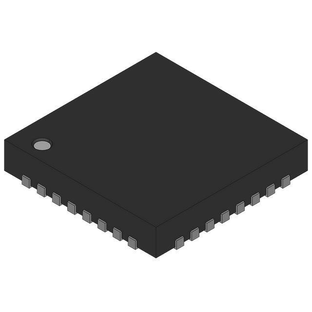
QFN31 5x5
CASE 485FG
Capable of Average Currents up to 25 A
Capable of Peak Currents up to 65 A
Over 97% Peak−Efficiency
Compatible with 3.3 V and 5 V PWM Inputs, with Tri−State
Zero Current Detection for Improving Light Load Efficiency
Optional Thermal Shutdown Protection
♦ NCP81391: With Thermal Shutdown
♦ NCP81391A: No Thermal Shutdown
Internal Bootstrap Diode
Undervoltage Lockout
This is a Pb−Free Device
VIN17
•
•
•
•
•
•
81391
ALYWG
G
(Top View)
Figure 1. Application Diagram (Buck−Boost)
ORDERING INFORMATION
This document contains information on a new product. Specifications and information
herein are subject to change without notice.
Device
NCP81391MNTXG
NCP81391AMNTXG
Package
Shipping†
QFN31
(Pb−Free)
2500 / Tape &
Reel
†For information on tape and reel specifications,
including part orientation and tape sizes, please
refer to our Tape and Reel Packaging Specification
Brochure, BRD8011/D.
© Semiconductor Components Industries, LLC, 2017
August, 2017 − Rev. P0
1
Publication Order Number:
NCP81391/D
�NCP81391, NCP81391A
GH
BST
VCCD
VIN
VCC
3.84V
LEVEL
SHIFT
UVLO
SHUTDOWN
DEAD
TIME
CNTRL
PWM
3.84V
ZCD_EN#
PHASE
45k
Clip
Temp
Sense
VSWH
For NCP81391/
No TSD for
NCP81391A
LOGIC
LEVEL
SHIFT
VSWH
45k
PGND
EN
For NCP81391/
No resistor for
NCP81391A
GLD GLF
CGND
Figure 2. Simplified Block Diagram
Table 1. PIN LIST AND DESCRIPTIONS
Pin No.
Symbol
Description
1
PHASE
Bootstrap Capacitor Return
2
PGND2
Power Ground
3
CGND
Signal Ground
4
EN
5
PWM
6
ZCD_EN#
7
VCC
Control Power Supply Input
8
VCCD
Driver Power Supply Input
9
NC9
No Connect
10
BST
Bootstrap Supply Voltage. Connect a MLCC capacitor of at least 0.1 mF from this pin to PHASE.
High−Side MOSFET Gate Access. Leave floating.
Enable. There is a pull−down resistor to CGND for the NCP81391. No pull−down resistor for NCP81391A.
PWM Control Input:
PWM = High ³ HS FET is on, LS FET is off
PWM = Mid ³ HS FET is off, LS FET is off
PWM = Low, ZCD_EN# = High ³ HS FET is off, LS FET is on
PWM = Low, ZCD_EN# = Low ³ HS FET is off, LS FET is off when zero current is detected
Zero Current Detect Control. When this pin is at logic low, low−side FET will turn off when zero inductor
current is detected (after a minimum blanking/de−bounce time). There is an internal pull−up resistor.
11
GH
12
NC12
No Connect
13
VIN13
Conversion Supply Power Input
14
VIN14
Conversion Supply Power Input
15
VIN15
Conversion Supply Power Input
www.onsemi.com
2
�NCP81391, NCP81391A
Table 1. PIN LIST AND DESCRIPTIONS
Pin No.
Symbol
Description
16
VIN16
Conversion Supply Power Input
17
VIN17
Conversion Supply Power Input
18
VIN18
Conversion Supply Power Input
19
VIN19
Conversion Supply Power Input
20
PGND20
Power Ground
21
PGND21
Power Ground
22
PGND22
Power Ground
23
PGND23
Power Ground
24
VSWH24
Switch Node Output
25
VSWH25
Switch Node Output
26
VSWH26
Switch Node Output
27
VSWH27
Switch Node Output
28
GLF28
Low−Side MOSFET Gate Access. Pins 28, 29, 30 and 31 must be connected together on the PCB.
29
GLF29
Low−Side MOSFET Gate Access. Pins 28, 29, 30 and 31 must be connected together on the PCB.
30
GLD30
Low−Side Driver Gate Access. Pins 28, 29, 30 and 31 must be connected together on the PCB.
31
GLD31
Low−Side Driver Gate Access. Pins 28, 29, 30 and 31 must be connected together on the PCB.
32
PGND32
33
VIN33
Conversion Supply Power Input Flag
34
GL34
Low Side MOSFET Gate Access. Do not connect to PCB. See Recommended PCB Footprint for details.
Power Ground Flag
Table 2. ABSOLUTE MAXIMUM RATINGS (Electrical Information – all signals referenced to PGND unless noted otherwise)
Pin Name
VMIN
VMAX
Unit
−0.3
13.2
V
−
15
V
VIN
−0.3
30
V
BST (DC)
−0.3
35
V
BST (< 10 ns)
−0.3
40
V
BST to PH (DC)
−0.3
13.2
V
VSWH, PHASE (DC)
−0.3
30
V
VSWH, PHASE (< 10 ns)
−5
35
V
GH (DC)
−
VBST + 0.3
V
−0.3
13.2
V
−2
−
V
VCC, VCCD (DC)
VCC, VCCD (< 100 ns)
GH wrt/ VSWH (DC)
GH wrt/ VSWH (< 200 ns)
GH wrt/ VSWH (< 100 ns)
−
15
V
−0.3
VVCC + 0.3
V
GL (< 200 ns)
−5
−
V
GL (< 100 ns)
−
15
V
−0.3
6.5
V
GL (DC)
EN, ZCD_EN#, PWM
Stresses exceeding those listed in the Maximum Ratings table may damage the device. If any of these limits are exceeded, device functionality
should not be assumed, damage may occur and reliability may be affected.
www.onsemi.com
3
�NCP81391, NCP81391A
Table 3. THERMAL INFORMATION
Rating
Symbol
Value
Unit
qJ−A
23
°C/W
RyJ−BT
0.3
°C/W
RyJ−CT
0.5
°C/W
Operating Junction Temperature Range (Note 2)
TJ
−40 to +150
°C
Operating Ambient Temperature Range
TA
−40 to +125
°C
Maximum Storage Temperature Range
TSTG
−40 to +150
°C
PD
5.4
W
MSL
3
Thermal Resistance (Note 1)
Maximum Power Dissipation
Moisture Sensitivity Level
1. JESD 51-7 (2S2P Direct-Attach Method) with 0 LFM
2. The maximum package power dissipation must be observed.
Table 4. RECOMMENDED OPERATING CONDITIONS
Parameter
Supply Voltage Range
Conversion Voltage
Pin Name
Conditions
Min
Typ
Max
Unit
VCC, VCCD
4.5
12
13.2
V
VIN
4.5
12
20
V
FSW = 250 kHz
25
A
FSW = 250 kHz, VVIN = 12 V, VOUT =
6 V, Duration = 10 ms, Period = 1 s
65
A
100
°C
Continuous Output Current
Peak Output Current
Operating Temperature
−40
Functional operation above the stresses listed in the Recommended Operating Ranges is not implied. Extended exposure to stresses beyond
the Recommended Operating Ranges limits may affect device reliability.
Table 5. ELECTRICAL CHARACTERISTICS
(VVCC = VVCCD = 12 V, VVIN = 12 V, VEN = 5.0 V, CVCCD = CVCC = 0.1 mF unless specified otherwise) Min/Max values are valid for the
temperature range −40°C ≤ TA ≤ 100°C unless noted otherwise, and are guaranteed by test, design or statistical correlation.)
Parameter
Symbol
Conditions
Min
Typ
Max
Unit
EN = 5 V, PWM = 250 kHz
−
−
2
mA
IVCC_EN
EN# = 5 V, PWM = 0 V, ZCD_EN# = 5 V
−
−
2
mA
IVCC_ZCD
EN# = 5 V, PWM = 0 V, ZCD_EN# = 0 V
−
−
2
mA
IVCC_DIS
EN = 0 V, ZCD_EN# = 5 V
−
960
1500
mA
IVCC_DIS_ZCD EN = 0 V, ZCD_EN# = 0 V
−
960
1500
mA
VCC
Operating Current
Enabled, No switching
Disabled Current
IVCC_PWM
UVLO Threshold
VUVLO
UVLO Hysteresis
VUVLO_HYS
VCC rising
3.8
4.35
4.5
V
150
200
−
mV
−
47
70
mA
VCCD SUPPLY CURRENT
Operating
Enabled, No switching
Disabled
IVCCD_PWM
IVCCD_EN
IVCCD_DIS
EN = 5 V, PWM = 250 kHz
EN = 5 V, PWM = 0 V
NCP81391
−
−
100
mA
EN = 5 V, PWM = 0 V
NCP81391A
−
−
100
mA
−
60
100
mA
EN = 0 V
PWM INPUT
Input High Voltage
VPWM_HI
2.6
−
−
V
Input Mid Voltage
VPWM_MID
1.4
−
1.8
V
Input Low Voltage
VPWM_LO
−
−
0.6
V
RPWM
−
162
−
kW
−
1.6
−
V
PWM Input Resistance
PWM Input Bias Voltage
VPWM_BIAS
PWM pin is floating
www.onsemi.com
4
�NCP81391, NCP81391A
Table 5. ELECTRICAL CHARACTERISTICS
(VVCC = VVCCD = 12 V, VVIN = 12 V, VEN = 5.0 V, CVCCD = CVCC = 0.1 mF unless specified otherwise) Min/Max values are valid for the
temperature range −40°C ≤ TA ≤ 100°C unless noted otherwise, and are guaranteed by test, design or statistical correlation.)
Parameter
Symbol
Conditions
Min
Typ
Max
Unit
−
−
5
mA
PWM = Low to GH−VSWH falling @ 90%
−
18
24
PWM INPUT
IPWM_LK
Input Leakage
HIGH SIDE DRIVER
Propagation Delay, PWM Falling
TPWM,PD_F
Non−overlap Delay, Leading Edge
(Note 3)
TNOL_L
GL falling @ 1 V to
GH−VSWH rising @ 1 V
6
13
20
ns
Fall Time, High−Side Gate
tfDRVH
GH falling, 90% to 10%
−
3.5
−
ns
Rise Time, High−Side Gate
trDRVH
GH rising, 10% to 90%
−
10
−
ns
Entering PWM Mid-state Propagation TPWM_ENTER_H PWM = High−to−Mid to GH−VSWH falling
@ 90%
Delay, High-to−Mid
−
20
−
ns
TPWM_EXIT_H PWM = Mid−to−High to GH−VSWH rising
@ 10%
−
13
25
ns
PWM = High to GL falling @ 90%
−
15
22
ns
Exiting PWM Mid-state Propagation
Delay, Mid-to−High
LOW SIDE DRIVER
Propagation Delay, PWM Rising
TPWM,PD_R
Non−overlap Delay, Trailing Edge
(Note 3)
TNOL_T
GH−VSWH falling @ 1 V to
GL rising @ 1 V
5
16
21
ns
Fall Time, Low−Side Gate
tfDRVL
GL falling, 90% to 10%
−
13
−
ns
Rise Time, Low−Side Gate
trDRVL
GL rising, 10% to 90%
−
2.8
−
ns
Entering PWM Mid-state Propagation TPWM_ENTER_L PWM = Low−to−Mid to GL falling @ 90%
Delay, Low-to−Mid
−
30
−
ns
TPWM_EXIT_L PWM = Mid−to−Low to GL rising @ 10%
−
13
25
ns
Exiting PWM Mid-state Propagation
Delay, Mid-to−Low
MOSFET
N−Channel High−Side MOSFET On
Resistance
RON_HS
From VIN to VSWH pin
−
2.0
−
mW
N−Channel Low−Side MOSFET On
Resistance
RON_LS
From VSWH to PGND pin
−
1.7
−
mW
IEN_LK
NCP8139
−
20
−
mA
NCP8139A
−
50
−
nA
EN INPUT
Input Leakage
Upper Threshold
VEN_HI
2.0
−
−
V
Lower Threshold
VEN_LO
−
−
0.8
V
Hysteresis
VEN_HYS
VEN_HI – VEN_LO
−
470
−
mV
Pull−down resistance to CGND
−
300
−
kW
EN Input Resistance
(NCP81391 Only)
REN
Enable Delay Time
TEN_ON
EN rising @ VEN_HI to GH−VSWH rising @
10%, PWM = High
−
30
−
ns
Disable Delay Time
TEN_OFF
EN falling @ VEN_LO to GL falling @ 90%,
PWM = Low
−
15
40
ns
ZERO CURRENT DETECTION ENABLE
ZCD_EN# High
VZCD_ENB_HI
2.0
−
−
V
ZCD_EN# Low
VZCD_ENB_LO
−
−
0.8
V
Hysteresis
VZCD_ENB_HYS
−
470
−
mV
−
725
−
kW
−
−3
−
mV
ZCD_EN# Input Resistance
ZCD Threshold
RZCD_ENB
Pull−up resistance to internal 3.84 V
VZCD_ENB_TH ZCD_EN# = 0 V, PWM = 0 V
www.onsemi.com
5
�NCP81391, NCP81391A
Table 5. ELECTRICAL CHARACTERISTICS
(VVCC = VVCCD = 12 V, VVIN = 12 V, VEN = 5.0 V, CVCCD = CVCC = 0.1 mF unless specified otherwise) Min/Max values are valid for the
temperature range −40°C ≤ TA ≤ 100°C unless noted otherwise, and are guaranteed by test, design or statistical correlation.)
Parameter
Symbol
Conditions
Min
Typ
Max
Unit
−
130
−
ns
−
170
−
°C
−
20
−
°C
0.1
0.4
0.6
V
ZERO CURRENT DETECTION ENABLE
ZCD Blanking + De−Bounce Timer
TBLANK
THERMAL SHUTDOWN (For NCP81391 Only)
Thermal Shutdown Temperature
Thermal Shutdown Hysteresis
TTHDN
Temperature at Driver Die
TTHDN_HYS
BOOSTSTRAP DIODE
Forward Voltage
VF_BST
Forward Bias Current = 2.0 mA
Product parametric performance is indicated in the Electrical Characteristics for the listed test conditions, unless otherwise noted. Product
performance may not be indicated by the Electrical Characteristics if operated under different conditions.
3. Guaranteed by design and/or characterization. This parameter is not tested in production.
www.onsemi.com
6
�NCP81391, NCP81391A
TYPICAL CHARACTERISTICS
Figure 3. Efficiency − 12 V Input, 500 kHz
Figure 4. Power Loss − 12 V Input, 500 kHz
Figure 5. Efficiency − 12 V Input, 250 kHz
Figure 6. Power Loss − 12 V Input, 250 kHz
Figure 7. Output Current Derating
fSW = 250 kHz; VIN = 12 V; VCC = VCCD = 12 V; VOUT = 6 V; L = 720 nH
www.onsemi.com
7
�NCP81391, NCP81391A
APPLICATIONS INFORMATION
Three−State PWM Input
Theory of Operation
Switching PWM between logic−high and logic−low states
allows the driver to operate in continuous conduction mode,
as long as VCC is greater than the UVLO threshold and EN
is high.
The PWM mid−state allows the NCP81391/A to enter a
high−impedance mode, where both MOSFETs are off.
Low−Side Driver
The low−side driver drives a ground−referenced
low−RDS(on) N−Channel MOSFET. The voltage rail for the
low−side driver is internally connected to VCCD and
CGND.
The GLD pin connects directly to the output of the
low−side driver. The GLF pins connects directly to the gate
of the low−side MOSFET. See Figure 2. GLD and GLF are
not connected inside the package. For proper operation,
these pins must be connected together on the PCB.
Table 6. EN/PWM LOGIC TABLE
High−Side Driver
The high−side driver drives a floating low−RDS(on)
N−channel MOSFET. The gate voltage for the high−side
driver is developed by a bootstrap circuit referenced to the
PHASE pin, which is internally connected to the VSWH pin.
The bootstrap circuit is comprised of an internal diode and
an external bootstrap capacitor. When the NCP81391/A is
starting up, the VSWH pin is at ground, so the bootstrap
capacitor charges up to VCCD through the bootstrap diode
(see Figure 1). When the PWM input goes high, the
high−side driver will begin to turn on the high−side
MOSFET using the stored charge of the bootstrap capacitor.
As the high−side MOSFET turns on, the voltage at the
VSWH pin rises. When the high−side MOSFET is fully on,
the VSWH voltage equals the VIN voltage, with the BST
voltage higher than VIN by the amount of voltage on the
bootstrap capacitor. The bootstrap capacitor is recharged
when the switch node goes low during the next cycle.
Parasitic inductances and capacitances within the
packaging and MOSFETs can cause significant ringing of
the VSWH signal during turn−on and turn−off of the
high−side MOSFET. When operating at high input voltages
and high output currents, the peak ringing voltages on
VSWH could cause the drain−to−source voltage across the
MOSFETs to exceed its maximum rating. Including a
resistor in series with the bootstrap capacitor can reduce the
peak VSWH ringing voltages. A resistor value of 4 W is
recommended when operating at VIN voltages greater than
16 V.
EN
PWM
ZCD_EN#
GH
GL
LOW
X
X
LOW
LOW
HIGH
LOW
HIGH
LOW
HIGH
HIGH
MID
HIGH
LOW
LOW
HIGH
HIGH
HIGH
HIGH
LOW
HIGH
LOW
LOW
LOW
ZCD
HIGH
MID
LOW
LOW
LOW
HIGH
HIGH
LOW
HIGH
LOW
Zero Current Detection
At light load conditions, the inductor current can be
negative due to the inductor current ripple. The zero current
detection (ZCD) function in the NCP81391/A can prevent
negative current during these light load conditions. When
ZCD is active, the NCP81391/A will monitor the voltage at
the VSWH pins when the LS FET is on and conducting.
There is a blanking/de−bounce timer that delays when this
monitoring starts, from the time GL goes high. As the
inductor current falls towards zero, the voltage on VSWH
will become less negative. When the VSWH voltage reaches
the ZCD threshold, the LS FET is turned off. Positive current
can still flow through the body diode of the LS FET, but the
body diode will block any current in the negative direction.
ZCD is activated by placing ZCD_EN# in the logic−low
state. There is an internal pull−up resistor at the ZCD_EN#
pin.
Whenever VCC rises above the UVLO threshold, an
auto−calibration is conducted on the ZCD Threshold.
During the auto−calibration, the driver outputs will remain
low and not respond to the PWM input. The auto−calibration
cycle takes 28 ms to complete, typically.
Overlap Protection Circuit
Thermal Shutdown
As PWM transitions between the logic high and logic low
states, the driver circuitry prevents both MOSFETs from
being on at the same time. While one MOSFET is turned off,
the driver monitors the gate voltage of that MOSFET until
it reaches 1 V. At this point, a non−overlap timer is started,
and prevents the gate of the other MOSFET from going high
until this timer expires. In the electrical characteristics table,
this non−overlap timer is specified as the time between 1 V
of the falling gate and 10% of the high value of the rising
gate.
With the NCP81391, if the driver temperature exceeds
TTHDN, the part will enter thermal shutdown and turn off
both MOSFETs. After the temperature decreases to TTHDN
− TTHDN_HYS, the part will resume normal operation.
For applications that prefer not to have this power stage
have a thermal shutdown, the NCP81391A removes the
thermal shutdown protection feature.
To distinguish between the NCP81391 and NCP81391A,
externally, the NCP81391 has an internal pull−down resistor
at the EN pin while the NCP81391A does not have an
internal pull−down resistor at the EN pin.
www.onsemi.com
8
�NCP81391, NCP81391A
Power Supply Decoupling
maximum duty cycle must be respected. The maximum duty
cycle depends on the two time constants that appear during
the charging time (converter’s toff) and discharging time
(converter’s ton). To keep the bootstrap capacitor charged,
the following relation must kept.
The NCP81391/A sources relatively large currents into
the MOSFET gates. In order to maintain a constant and
stable input supply voltage, low−ESR capacitors should be
placed between VCC and GND and between VCCD and
ground, close to the NCP81391/A. A 1 mF to 4.7 mF
multilayer ceramic capacitor (MLCC) is sufficient. To
further filter noise from VCCD from entering the VCC pin,
placing a 10 W resistor between the VCC and VCCD pins is
recommended.
D@
Thus, Dmax can be expressed as
Dmax + 1 *
Bootstrap Circuit
Rbst
Rdrv ) Rbst
50
With the converter’s duty cycle, Rdrv the High−Side
Driver equivalent resistance from VBST to VSWH
(typically 5 kW), Rbst the bootstrap series resistor. Note that
the bootstrap capacitance has no effect on maximum duty
cycle since it is common in both time constants.
Example:
fsw = 250 kHz, Rdrv = 5 kW, Rbst = 4 W, the maximum duty
cycle allowed to keep the bootstrap capacitor charged is
Dmax = 96% and ton_max = Dmax/fsw = 3.84 ms.
The bootstrap circuit uses an external charge storage
capacitor (CBST) and the internal bootstrap diode. The
bootstrap capacitor should have a voltage rating twice the
maximum VCCD supply voltage. A bootstrap capacitance
of at least 100 nF with a minimum 25 V rating is
recommended. For best performances, use a 1 mF ceramic
capacitor.
In order to prevent the bootstrap capacitor from
discharging during conditions where the high side is turned
on for a long time, such as high duty cycle or ZCD, a
PWM
Rdrv
u 50
(1 * D) @ Rbst
TPWM,PD_R tfDRVL
GL
90%
90%
1V
10%
TPWM,PD_F
TNOL_L
tfDRVH
trDRVH
90%
GH −
VSWH
1V
90%
10%
1V
10%
Figure 8. Gate Timing Diagram
www.onsemi.com
9
10%
1 V trDRVL
TNOL_T
�NCP81391, NCP81391A
Inductor
Current
0A
ZCD_EN# = High allows
negative current
ZCD_EN#
0V
ZCD_EN# & PWM = Low
prevents negative current
PWM
0V
PWM = Mid puts device into
high−impedance state
GH
0V
GL stays low with PWM
in mid−state
GL
0V
GL pulls low when zero current is
detected
Figure 9. Zero Cross Detect Functionality
Figure 10. Application Schematic (Buck−Side)
www.onsemi.com
10
�NCP81391, NCP81391A
Figure 11. Recommended Layout (Buck−Side)
www.onsemi.com
11
�MECHANICAL CASE OUTLINE
PACKAGE DIMENSIONS
QFN31 5x5, 0.5P
CASE 485FG
ISSUE A
DATE 27 JUL 2017
SCALE 2:1
GENERIC
MARKING DIAGRAM*
1
XXXXXXXX
XXXXXXXX
AWLYYWWG
G
XXXXX = Specific Device Code
A
= Assembly Location
WL
= Wafer Lot
YY
= Year
WW
= Work Week
G
= Pb−Free Package
(Note: Microdot may be in either location)
*This information is generic. Please refer
to device data sheet for actual part
marking.
Pb−Free indicator, “G” or microdot “ G”,
may or may not be present.
DOCUMENT NUMBER:
DESCRIPTION:
98AON17080G
QFN31 5x5, 0.5P
Electronic versions are uncontrolled except when accessed directly from the Document Repository.
Printed versions are uncontrolled except when stamped “CONTROLLED COPY” in red.
PAGE 1 OF 1
ON Semiconductor and
are trademarks of Semiconductor Components Industries, LLC dba ON Semiconductor or its subsidiaries in the United States and/or other countries.
ON Semiconductor reserves the right to make changes without further notice to any products herein. ON Semiconductor makes no warranty, representation or guarantee regarding
the suitability of its products for any particular purpose, nor does ON Semiconductor assume any liability arising out of the application or use of any product or circuit, and specifically
disclaims any and all liability, including without limitation special, consequential or incidental damages. ON Semiconductor does not convey any license under its patent rights nor the
rights of others.
© Semiconductor Components Industries, LLC, 2019
www.onsemi.com
�onsemi,
, and other names, marks, and brands are registered and/or common law trademarks of Semiconductor Components Industries, LLC dba “onsemi” or its affiliates
and/or subsidiaries in the United States and/or other countries. onsemi owns the rights to a number of patents, trademarks, copyrights, trade secrets, and other intellectual property.
A listing of onsemi’s product/patent coverage may be accessed at www.onsemi.com/site/pdf/Patent−Marking.pdf. onsemi reserves the right to make changes at any time to any
products or information herein, without notice. The information herein is provided “as−is” and onsemi makes no warranty, representation or guarantee regarding the accuracy of the
information, product features, availability, functionality, or suitability of its products for any particular purpose, nor does onsemi assume any liability arising out of the application or use
of any product or circuit, and specifically disclaims any and all liability, including without limitation special, consequential or incidental damages. Buyer is responsible for its products
and applications using onsemi products, including compliance with all laws, regulations and safety requirements or standards, regardless of any support or applications information
provided by onsemi. “Typical” parameters which may be provided in onsemi data sheets and/or specifications can and do vary in different applications and actual performance may
vary over time. All operating parameters, including “Typicals” must be validated for each customer application by customer’s technical experts. onsemi does not convey any license
under any of its intellectual property rights nor the rights of others. onsemi products are not designed, intended, or authorized for use as a critical component in life support systems
or any FDA Class 3 medical devices or medical devices with a same or similar classification in a foreign jurisdiction or any devices intended for implantation in the human body. Should
Buyer purchase or use onsemi products for any such unintended or unauthorized application, Buyer shall indemnify and hold onsemi and its officers, employees, subsidiaries, affiliates,
and distributors harmless against all claims, costs, damages, and expenses, and reasonable attorney fees arising out of, directly or indirectly, any claim of personal injury or death
associated with such unintended or unauthorized use, even if such claim alleges that onsemi was negligent regarding the design or manufacture of the part. onsemi is an Equal
Opportunity/Affirmative Action Employer. This literature is subject to all applicable copyright laws and is not for resale in any manner.
PUBLICATION ORDERING INFORMATION
LITERATURE FULFILLMENT:
Email Requests to: orderlit@onsemi.com
onsemi Website: www.onsemi.com
◊
TECHNICAL SUPPORT
North American Technical Support:
Voice Mail: 1 800−282−9855 Toll Free USA/Canada
Phone: 011 421 33 790 2910
Europe, Middle East and Africa Technical Support:
Phone: 00421 33 790 2910
For additional information, please contact your local Sales Representative
�