NCS2004, NCS2004A
Operational Amplifier,
Rail-to-Rail, 3.5 MHz,
Wide Supply
The NCS2004 operational amplifier provides rail−to−rail output
operation. The output can swing within 70 mV to the positive rail and
30 mV to the negative rail. This rail−to−rail operation enables the user
to make optimal use of the entire supply voltage range while taking
advantage of 3.5 MHz bandwidth. The NCS2004 can operate on
supply voltage as low as 2.5 V over the temperature range of −40°C to
125°C. The high bandwidth provides a slew rate of 2.4 V/ms while
only consuming a typical 390 mA of quiescent current. Likewise the
NCS2004 can run on a supply voltage as high as 16 V making it ideal
for a broad range of battery operated applications. Since this is a
CMOS device it has high input impedance and low bias currents
making it ideal for interfacing to a wide variety of signal sensors. In
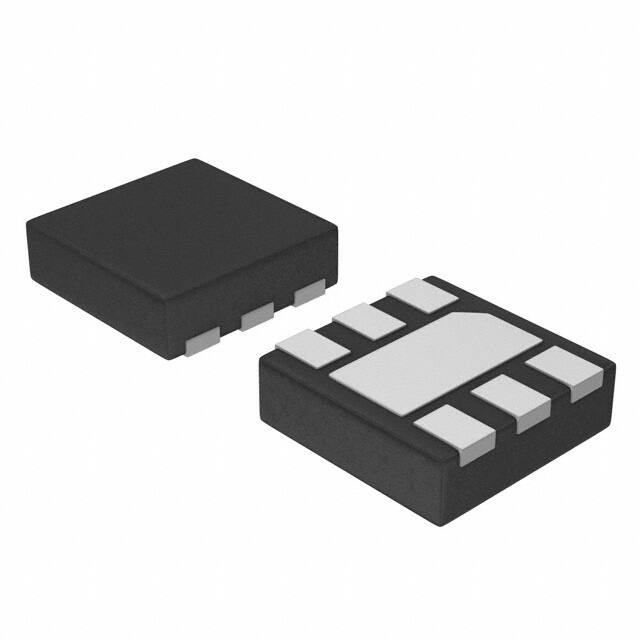
addition it comes in either a small SC−88A or UDFN package
allowing for use in high density PCB’s.
Features
•
•
•
•
•
•
•
•
•
www.onsemi.com
MARKING DIAGRAMS
SC−88A
(SC−70−5)
SN SUFFIX
CASE 419A
ADK MG
G
ADK = Specific Device Code
M
= Date Code
G
= Pb−Free Package
(Note: Microdot may be in either location)
1
6
UDFN6
CASE 517AP
xx MG
G
1
Rail−To−Rail Output
Wide Bandwidth: 3.5 MHz
High Slew Rate: 2.4 V/ms
Wide Power Supply Range: 2.5 V to 16 V
Low Supply Current: 390 mA
Low Input Bias Current: 45 pA
Wide Temperature Range: −40°C to 125°C
Small Packages: 5−Pin SC−88A and UDFN6 1.6x1.6
These Devices are Pb−Free, Halogen Free/BFR Free and are RoHS
Compliant
xx = Specific Device Code
AA for NCS2004
AC for NCS2004A
M = Date Code
G = Pb−Free Package
(Note: Microdot may be in either location)
PIN CONNECTIONS
5 VDD
IN+ 1
+
−
VSS 2
IN−
4 OUT
3
Applications
• Notebook Computers
• Portable Instruments
SC−88A (Top View)
VSS
1
NC
2
IN−
3
6 OUT
− +
5 VDD
4 IN+
UDFN (Top View)
ORDERING INFORMATION
Device
Package
Shipping†
NCS2004SQ3T2G
SC−88A
(Pb−Free)
3000 /
Tape & Reel
NCS2004MUTAG,
NCS2004AMUTAG
UDFN6
(Pb−Free)
3000 /
Tape & Reel
†For information on tape and reel specifications,
including part orientation and tape sizes, please
refer to our Tape and Reel Packaging Specifications
Brochure, BRD8011/D.
© Semiconductor Components Industries, LLC, 2015
October, 2015 − Rev. 9
1
Publication Order Number:
NCS2004/D
�NCS2004, NCS2004A
MAXIMUM RATINGS
Symbol
Rating
Value
Unit
16.5
V
Input Differential Voltage
$Supply Voltage
V
VI
Input Common Mode Voltage Range
−0.2 V to (VDD +
0.2 V)
V
II
Maximum Input Current
$10
mA
IO
Output Current Range
$100
mA
Continuous Total Power Dissipation (Note 1)
200
mW
TJ
Maximum Junction Temperature
150
°C
qJA
Thermal Resistance
333
°C/W
Tstg
Operating Temperature Range (free−air)
−40 to 125
°C
Tstg
Storage Temperature
VDD
Supply Voltage
VID
VESD
−65 to 150
°C
Mounting Temperature (Infrared or Convection − 20 sec)
260
°C
Machine Model
Human Body Model
300
2000
V
Stresses exceeding those listed in the Maximum Ratings table may damage the device. If any of these limits are exceeded, device
functionality should not be assumed, damage may occur and reliability may be affected.
1. Continuous short circuit operation to ground at elevated ambient temperature can result in exceeding the maximum allowed junction
temperature of 150°C. Output currents in excess of 45 mA over long term may adversely affect reliability. Shorting output to either V+
or V− will adversely affect reliability.
DC ELECTRICAL CHARACTERISTICS (VDD = 2.5 V, 3.3 V, 5 V and $5 V, TA = 25°C, RL w 10 kW unless otherwise noted)
Parameter
Symbol
Input Offset Voltage
(NCS2004)
VIO
Input Offset Voltage
(NCS2004A)
VIO
Offset Voltage Drift
ICVOS
VIC = VDD/2, VO = VDD/2, RL = 10 kW, RS = 50 W
Common Mode
Rejection Ratio
CMRR
0 V v VIC v VDD − 1.35 V, RS = 50 W
Conditions
Min
VIC = VDD/2, VO = VDD/2, RL = 10 kW, RS = 50 W
5.0
mV
3.0
TA = −40°C to +125°C
5.0
VDD = 2.5 V
55
mV
2.0
mV/°C
94
dB
52
VDD = 5 V
65
130
62
0 V v VIC v VDD − 1.35 V, RS = 50 W
AVD
0.5
7.0
TA = −40°C to +125°C
Large Signal
Voltage Gain
Unit
VIC = VDD/2, VO = VDD/2, RL = 10 kW, RS = 50 W
0 V v VIC v VDD − 1.35 V, RS = 50 W
PSRR
Max
TA = −40°C to +125°C
TA = −40°C to +125°C
Power Supply
Rejection Ratio
Typ
VDD = $5 V
69
TA = −40°C to +125°C
66
VDD = 2.5 V to 16 V, VIC = VDD/2, No Load
70
TA = −40°C to +125°C
65
VDD = 2.5 V
VO(pp) = VDD/2, RL = 10 kW
TA = −40°C to +125°C
90
140
135
dB
130
dB
76
VDD = 3.3 V
VO(pp) = VDD/2, RL = 10 kW
TA = −40°C to +125°C
92
123
76
VDD = 5 V
VO(pp) = VDD/2, RL = 10 kW
TA = −40°C to +125°C
95
127
86
VDD = $5 V
VO(pp) = VDD/2, RL = 10 kW
TA = −40°C to +125°C
95
90
www.onsemi.com
2
130
�NCS2004, NCS2004A
DC ELECTRICAL CHARACTERISTICS (VDD = 2.5 V, 3.3 V, 5 V and $5 V, TA = 25°C, RL w 10 kW unless otherwise noted)
Parameter
Symbol
Input Bias Current
IB
Input Offset Current
IIO
Conditions
VDD = 5 V, VIC = VDD/2, VO = VDD/2,
RS = 50 W
VDD = 5 V, VIC = VDD/2, VO = VDD/2,
RS = 50 W
Differential Input
Resistance
ri(d)
Common−mode
Input Capacitance
CIC
f = 21 kHz
Output Swing
(High−level)
VOH
VIC = VDD/2, IOH = −1 mA
Min
TA = 25°C
Unit
45
150
pA
1000
TA = 25°C
45
TA = 125°C
TA = −40°C to +125°C
150
pA
1000
2.35
1000
GW
8.0
pF
2.43
V
2.28
VDD = 3.3 V
TA = −40°C to +125°C
3.15
3.21
3.00
VDD = 5 V
VIC = VDD/2, IOH = −1 mA
TA = −40°C to +125°C
4.8
4.93
4.75
VDD = $5 V
VIC = VDD/2, IOH = −1 mA
TA = −40°C to +125°C
4.92
4.96
4.9
VDD = 2.5 V
VIC = VDD/2, IOH = −5 mA
TA = −40°C to +125°C
1.7
V
2.14
1.5
VDD = 3.3 V
VIC = VDD/2, IOH = −5 mA
TA = −40°C to +125°C
2.5
2.89
2.1
VDD = 5 V
VIC = VDD/2, IOH = −5 mA
TA = −40°C to +125°C
4.5
4.68
4.35
VDD = $5 V
VIC = VDD/2, IOH = −5 mA
TA = −40°C to +125°C
VOL
Max
TA = 125°C
VDD = 2.5 V
VIC = VDD/2, IOH = −1 mA
Output Swing
(Low−level)
Typ
4.7
4.78
4.65
VDD = 2.5 V
VIC = VDD/2, IOL = −1 mA
0.03
TA = −40°C to +125°C
0.15
V
0.22
VDD = 3.3 V
VIC = VDD/2, IOL = −1 mA
0.03
TA = −40°C to +125°C
0.15
0.22
VDD = 5 V
VIC = VDD/2, IOL = −1 mA
0.03
TA = −40°C to +125°C
0.1
0.15
VIC = VDD/2, IOL = −1 mA
VDD = $5 V
0.05
VDD = 2.5 V
0.15
TA = −40°C to +125°C
0.08
0.1
VIC = VDD/2, IOL = −5 mA
TA = −40°C to +125°C
0.7
1.1
VDD = 3.3 V
VIC = VDD/2, IOL = −5 mA
0.13
TA = −40°C to +125°C
0.7
1.1
VIC = VDD/2, IOL = −5 mA
VDD = 5 V
0.13
VDD = $5 V
0.16
TA = −40°C to +125°C
0.4
0.5
VIC = VDD/2, IOL = −5 mA
TA = −40°C to +125°C
0.3
0.35
www.onsemi.com
3
V
�NCS2004, NCS2004A
DC ELECTRICAL CHARACTERISTICS (VDD = 2.5 V, 3.3 V, 5 V and $5 V, TA = 25°C, RL w 10 kW unless otherwise noted)
Parameter
Symbol
Output Current
IO
Conditions
VO = 0.5 V from rail, VDD = 2.5 V
VO = 0.5 V from rail, VDD = 5 V
VO = 0.5 V from rail, VDD = 10 V
Power Supply
Quiescent Current
IDD
VO = VDD/2
Min
Typ
Positive rail
4.0
Negative rail
5.0
Positive rail
7.0
Negative rail
8.0
Positive rail
13
Max
mA
Negative rail
12
VDD = 2.5 V
380
560
VDD = 3.3 V
385
620
VDD = 5 V
390
660
VDD = 10 V
400
800
TA = −40°C to +125°C
Unit
mA
1000
AC ELECTRICAL CHARACTERISTICS (VDD = 2.5 V, 5 V, & $5 V, TA = 25°C, and RL w 10 kW unless otherwise noted)
Parameter
Symbol
Unity Gain
Bandwidth
UGBW
Slew Rate at Unity
Gain
SR
Conditions
RL = 2 kW, CL = 10 pF
VO(pp) = VDD/2, RL = 10 kW, CL = 50 pF
Min
VDD = 2.5 V
3.2
VDD = 5 V to
10 V
3.5
VDD = 2.5 V
TA = −40°C to +125°C
VDD = 5 V
TA = −40°C to +125°C
VDD = $5 V
TA = −40°C to +125°C
Gain Margin
Settling Time to
0.1%
Total Harmonic
Distortion plus
Noise
tS
THD+N
en
Input−Referred
Current Noise
in
MHz
V/mS
1.45
2.3
1.8
2.6
1.3
RL = 2 kW, CL = 10 pF
45
°
RL = 2 kW, CL = 10 pF
14
dB
mS
V−step(pp) = 1 V, AV = −1, RL = 2 kW,
CL = 10 pF
VDD = 2.5 V
2.9
V−step(pp) = 1 V, AV = −1, RL = 2 kW,
CL = 68 pF
VDD = 5 V,
$5 V
2.0
AV = 1
0.004
AV = 10
0.04
AV = 100
0.3
AV = 1
0.004
AV = 10
0.04
AV = 100
0.03
VDD = 2.5 V, VO(pp) = VDD/2, RL = 2 kW,
f = 10 kHz
VDD = 5 V, $ 5 V, VO(pp) = VDD/2,
RL = 2 kW, f = 10 kHz
Input−Referred
Voltage Noise
2.0
Unit
1.2
VO(pp) = VDD/2, RL = 10 kW, CL = 50 pF
qm
1.35
Max
1
VO(pp) = VDD/2, RL = 10 kW, CL = 50 pF
Phase Margin
Typ
f = 1 kHz
30
f = 10 kHz
20
f = 1 kHz
0.6
www.onsemi.com
4
%
nV/√Hz
fA/√Hz
�0
RL = 2 kW
25°C
−10
−20
CMRR (dB)
−30
−40
−50
2.5 V
−60
5V
2.7 V
−70
−80
−90
10 V
10
100
1k
10k
100k
1M
INPUT BIAS AND OFFSET CURRENT (pA)
NCS2004, NCS2004A
250
200
150
100
0
Input Offset
−50
−100
−40 −25 −10
20 35
50
65
80 95 110 125
FREE AIR TEMPERATURE (°C)
Figure 1. CMRR vs. Frequency
Figure 2. Input Bias and Offset Current vs.
Temperature
2.5
VDD = 2.5 V
HIGH LEVEL OUTPUT VOLTAGE (V)
LOW LEVEL OUTPUT VOLTAGE (V)
5
FREQUENCY (Hz)
2.5
25°C
105°C
2
1.5
−40°C
1
0.5
0
10
0
20
30
40
50
60
70
2
−40°C
1.5
25°C
105°C
1
0.5
0
0
10
20
30
40
50
LOW LEVEL OUTPUT CURRENT (mA)
Figure 3. 2.5 V VOL vs. Iout
Figure 4. 2.5 V VOH vs. Iout
3.3
HIGH LEVEL OUTPUT VOLTAGE (V)
25°C
2.7
105°C
2.4
2.1
1.8
−40°C
1.5
1.2
0.9
0.6
0.3
0
60
LOW LEVEL OUTPUT CURRENT (mA)
VDD = 3.3 V
3
0
VDD = 2.5 V
80
3.3
LOW LEVEL OUTPUT VOLTAGE (V)
Input Bias
50
10
20
30
40
50
60
70
80
90
80
VDD = 3.3 V
3
2.7
2.4
105°C
2.1
1.8
1.5
25°C
1.2
0.9
−40°C
0.6
0.3
0
0
10
20
30
40
50
60
70
HIGH LEVEL OUTPUT CURRENT (mA)
LOW LEVEL OUTPUT CURRENT (mA)
Figure 5. 3.3 V VOL vs. Iout
Figure 6. 3.3 V VOH vs. Iout
www.onsemi.com
5
70
80
90
�NCS2004, NCS2004A
5
VDD = 5.0 V
HIGH LEVEL OUTPUT VOLTAGE (V)
LOW LEVEL OUTPUT VOLTAGE (V)
5
105°C
4
3
−40°C
25°C
2
1
0
0
10
20
30
40
50
60
70
3
−40°C
2
25°C
105°C
1
0
0
10
20
30
40
50
60
70
LOW LEVEL OUTPUT CURRENT (mA)
HIGH LEVEL OUTPUT CURRENT (mA)
Figure 7. VOL vs. Iout
Figure 8. VOH vs. Iout
80
10
VDD = 10 V
9
HIGH LEVEL OUTPUT VOLTAGE (V)
LOW LEVEL OUTPUT VOLTAGE (V)
4
80
10
8
7
6
105°C
5
4
25°C
3
2
1
−40°C
0
0
10
20
30
40
50
60
70
80
VDD = 10 V
9
8
7
6
25°C
5
4
−40°C
3
105°C
2
1
0
0
10
20
30
40
50
60 70 80
90
100 110 120
LOW LEVEL OUTPUT CURRENT (mA)
HIGH LEVEL OUTPUT CURRENT (mA)
Figure 9. 10 V VOL vs. Iout
Figure 10. 10 V VOH vs. Iout
12
600
AV = 10
RL = 2k
CL = 10 pF
TA = 25°C
THD = 5%
VDD = 10 V
10
9
8
105°C
SUPPLY CURRENT / Ch (mA)
11
Vout P−P (V)
VDD = 5.0 V
7
6
VDD = 5 V
5
4
3
VDD = 2.7 V
2
VDD = 2.5 V
1
0
0.01
0.1
1
10
100
1k
500
−40°C
300
200
100
0
0
10k
25°C
400
2
4
6
8
10
12
14
16
FREQUENCY (kHz)
SUPPLY VOLTAGE (V)
Figure 11. Peak−to−Peak Output vs. Supply vs.
Frequency
Figure 12. Supply Current vs. Supply Voltage
www.onsemi.com
6
18
�NCS2004, NCS2004A
0
RL = 2 kW,
Input = 200 mVpp,
AV = 1,
VDD = 2.5 V to 10 V,
TA = 25°C
−10
−20
PSRR (dB)
−30
−40
−50
−60
−70
−80
−90
−100
−110
100
1k
10k
100k
FREQUENCY (Hz)
Figure 13. PSRR vs. Frequency
140
180
OPEN LOOP GAIN (dB)
100
80
Gain
10 V
60
40
Gain
5V
20
135
Phase
5V
90
Phase
10 V
45
Gain
2.7 V
0
PHASE MARGIN (°C)
Phase
2.7 V
120
−20
1
10
100
1k
10k
100k
0
10M
1M
FREQUENCY (Hz)
Figure 14. Open Loop Gain and Phase vs.
Frequency
4.5
4
10 V
5V
3.5
3
2.7 V
SR+ @ 105°C
SR− @ 105°C
SLEW RATE (V/ms)
FREQUENCY (MHz)
4
SR+ @ 25°C
2.5 V
2.5
3
2
SR− @ 25°C
SR− @ −40°C
1
SR+ @ −40°C
RL = 2k
CL = 10 pF
2
−40
0
−20
0
20
40
60
80
100
0
0.5
1
1.5
2
2.5
3
TEMPERATURE (°C)
SUPPLY VOLTAGE (V)
Figure 15. Gain Bandwidth Product vs.
Temperature
Figure 16. Slew Rate vs. Supply Voltage
www.onsemi.com
7
3.5
�NCS2004, NCS2004A
4
10k
SR+ 10 V
VOLTAGE NOISE (nV√Hz)
SLEW RATE (V/ms)
SR− 10 V
3
SR+ 2.7 V
VS = ±2.5 V
Vin = GND,
Av = 22 RTI
SR+ 5 V
SR− 5 V
SR− 2.7 V
2
1k
100
10
1
1
−60
−40 −20
0
20
40
60
80
100
120
1
10
100
1k
10k
FREE AIR TEMPERATURE (°C)
FREQUENCY (Hz)
Figure 17. Slew Rate vs. Temperature
Figure 18. Voltage Noise vs. Frequency
VS = ±1.25 V
Av = −1
RL = 2 kW
100k
250 mV/div
250 mV/div
VS = +2.5 V
Av = +1
RL = 2 kW
VS = ±1.25 V
Av = −1
RL = 2 kW
VS = +2.5 V
Av = +1
RL = 2 kW
25 mV/div
500 ns/div
Figure 20. 2.5 V Non−Inverting Large Signal
Pulse Response
25 mV/div
500 ns/div
Figure 19. 2.5 V Inverting Large Signal Pulse
Response
500 ns/div
500 ns/div
Figure 21. 2.5 V Inverting Small Signal Pulse
Response
Figure 22. 2.5 V Non−Inverting Small Signal
Pulse Response
www.onsemi.com
8
�NCS2004, NCS2004A
VS = +3 V
Av = +1
RL = 2 kW
250 mV/div
250 mV/div
VS = ±1.5 V
Av = −1
RL = 2 kW
Figure 23. 3 V Inverting Large Signal Pulse
Response
Figure 24. 3 V Non−Inverting Large Signal
Pulse Response
VS = ±1.5 V
Av = −1
RL = 2 kW
VS = +3 V
Av = +1
RL = 2 kW
25 mV/div
500 ns/div
25 mV/div
500 ns/div
500 ns/div
500 ns/div
Figure 25. 3 V Inverting Small Signal Pulse
Response
Figure 26. 3 V Non−Inverting Small Signal
Pulse Response
VS = ±3 V
Av = −1
RL = 2 kW
500 mV/div
500 mV/div
VS = +6 V
Av = +1
RL = 2 kW
500 ns/div
500 ns/div
Figure 27. 6 V Inverting Large Signal Pulse
Response
Figure 28. 6 V Non−Inverting Large Signal
Pulse Response
www.onsemi.com
9
�NCS2004, NCS2004A
VS = +6 V
Av = +1
RL = 2 kW
25 mV/div
25 mV/div
VS = +6 V
Av = −1
RL = 2 kW
500 ns/div
500 ns/div
Figure 29. 6 V Inverting Small Signal Pulse
Response
Figure 30. 6 V Non−Inverting Small Signal
Pulse Response
www.onsemi.com
10
�NCS2004, NCS2004A
APPLICATIONS
50 k
R1
5.0 k
VDD
VDD
R2
10 k
MC1403
VO
NCS2004
+
VO
NCS2004
VDD
−
Vref
−
+
fO +
1
V ref + V DD
2
2.5 V
R
R1
V O + 2.5 V(1 )
)
R2
R
Figure 31. Voltage Reference
C
C
1
2pRC
For: fo = 1.0 kHz
R = 16 kW
C = 0.01 mF
Figure 32. Wien Bridge Oscillator
VDD
C
R1
R3
C
−
Vin
CO
VO
NCS2004
+
R2
CO = 10 C
R2
Vref
Hysteresis
VOH
R1
Vref
Given: fo = center frequency
A(fo) = gain at center frequency
VO
+
NCS2004
Vin
VO
−
VOL
VinL
Choose value fo, C
Q
Then : R3 +
pf O C
VinH
Vref
R1 +
R1
(V OL * V ref) ) V ref
R1 ) R2
R1
V inH +
(V OH * V ref) ) V ref
R1 ) R2
R1
H+
(V OH * V OL)
R1 ) R2
V inL +
R2 +
R3
2 A(f O)
R1 R3
4Q 2 R1 * R3
For less than 10% error from operational amplifier,
((QO fO)/BW) < 0.1 where fo and BW are expressed in Hz.
If source impedance varies, filter may be preceded with
voltage follower buffer to stabilize filter parameters.
Figure 33. Comparator with Hysteresis
Figure 34. Multiple Feedback Bandpass Filter
www.onsemi.com
11
�MECHANICAL CASE OUTLINE
PACKAGE DIMENSIONS
SC−88A (SC−70−5/SOT−353)
CASE 419A−02
ISSUE L
SCALE 2:1
A
NOTES:
1. DIMENSIONING AND TOLERANCING
PER ANSI Y14.5M, 1982.
2. CONTROLLING DIMENSION: INCH.
3. 419A−01 OBSOLETE. NEW STANDARD
419A−02.
4. DIMENSIONS A AND B DO NOT INCLUDE
MOLD FLASH, PROTRUSIONS, OR GATE
BURRS.
G
5
4
−B−
S
1
2
DATE 17 JAN 2013
DIM
A
B
C
D
G
H
J
K
N
S
3
D 5 PL
0.2 (0.008)
B
M
M
N
INCHES
MIN
MAX
0.071
0.087
0.045
0.053
0.031
0.043
0.004
0.012
0.026 BSC
--0.004
0.004
0.010
0.004
0.012
0.008 REF
0.079
0.087
MILLIMETERS
MIN
MAX
1.80
2.20
1.15
1.35
0.80
1.10
0.10
0.30
0.65 BSC
--0.10
0.10
0.25
0.10
0.30
0.20 REF
2.00
2.20
J
GENERIC MARKING
DIAGRAM*
C
K
H
XXXMG
G
SOLDER FOOTPRINT
0.50
0.0197
XXX = Specific Device Code
M
= Date Code
G
= Pb−Free Package
0.65
0.025
0.65
0.025
0.40
0.0157
1.9
0.0748
SCALE 20:1
(Note: Microdot may be in either location)
*This information is generic. Please refer to
device data sheet for actual part marking.
Pb−Free indicator, “G” or microdot “G”, may
or may not be present. Some products may
not follow the Generic Marking.
mm Ǔ
ǒinches
STYLE 1:
PIN 1. BASE
2. EMITTER
3. BASE
4. COLLECTOR
5. COLLECTOR
STYLE 2:
PIN 1. ANODE
2. EMITTER
3. BASE
4. COLLECTOR
5. CATHODE
STYLE 3:
PIN 1. ANODE 1
2. N/C
3. ANODE 2
4. CATHODE 2
5. CATHODE 1
STYLE 4:
PIN 1. SOURCE 1
2. DRAIN 1/2
3. SOURCE 1
4. GATE 1
5. GATE 2
STYLE 6:
PIN 1. EMITTER 2
2. BASE 2
3. EMITTER 1
4. COLLECTOR
5. COLLECTOR 2/BASE 1
STYLE 7:
PIN 1. BASE
2. EMITTER
3. BASE
4. COLLECTOR
5. COLLECTOR
STYLE 8:
PIN 1. CATHODE
2. COLLECTOR
3. N/C
4. BASE
5. EMITTER
STYLE 9:
PIN 1. ANODE
2. CATHODE
3. ANODE
4. ANODE
5. ANODE
DOCUMENT NUMBER:
DESCRIPTION:
98ASB42984B
STYLE 5:
PIN 1. CATHODE
2. COMMON ANODE
3. CATHODE 2
4. CATHODE 3
5. CATHODE 4
Note: Please refer to datasheet for
style callout. If style type is not called
out in the datasheet refer to the device
datasheet pinout or pin assignment.
Electronic versions are uncontrolled except when accessed directly from the Document Repository.
Printed versions are uncontrolled except when stamped “CONTROLLED COPY” in red.
SC−88A (SC−70−5/SOT−353)
PAGE 1 OF 1
ON Semiconductor and
are trademarks of Semiconductor Components Industries, LLC dba ON Semiconductor or its subsidiaries in the United States and/or other countries.
ON Semiconductor reserves the right to make changes without further notice to any products herein. ON Semiconductor makes no warranty, representation or guarantee regarding
the suitability of its products for any particular purpose, nor does ON Semiconductor assume any liability arising out of the application or use of any product or circuit, and specifically
disclaims any and all liability, including without limitation special, consequential or incidental damages. ON Semiconductor does not convey any license under its patent rights nor the
rights of others.
© Semiconductor Components Industries, LLC, 2018
www.onsemi.com
�MECHANICAL CASE OUTLINE
PACKAGE DIMENSIONS
UDFN6 1.6x1.6, 0.5P
CASE 517AP
ISSUE O
6
1
SCALE 4:1
A
B
D
2X
0.10 C
PIN ONE
REFERENCE
2X
0.10 C
ÉÉ
ÉÉ
ÉÉ
DETAIL A
OPTIONAL
CONSTRUCTION
(A3)
DETAIL B
A
0.05 C
A1
0.05 C
SIDE VIEW
DETAIL A
6X
ÉÉÉ
ÉÉÉ
EXPOSED Cu
TOP VIEW
6X
C
A1
SEATING
PLANE
1
OPTIONAL
CONSTRUCTION
K
6
A3
DIM
A
A1
A3
b
D
E
e
D2
E2
K
L
L1
MILLIMETERS
MIN
MAX
0.45
0.55
0.00
0.05
0.13 REF
0.20
0.30
1.60 BSC
1.60 BSC
0.50 BSC
1.10
1.30
0.45
0.65
0.20
−−−
0.20
0.40
0.00
0.15
GENERIC
MARKING DIAGRAM*
1
XX MG
G
3
E2
6X
MOLD CMPD
DETAIL B
D2
L
NOTES:
1. DIMENSIONING AND TOLERANCING PER
ASME Y14.5M, 1994.
2. CONTROLLING DIMENSION: MILLIMETERS.
3. DIMENSION b APPLIES TO PLATED TERMINAL
AND IS MEASURED BETWEEN 0.15 AND
0.30 mm FROM TERMINAL.
4. COPLANARITY APPLIES TO THE EXPOSED
PAD AS WELL AS THE TERMINALS.
L
L1
E
DATE 26 OCT 2007
4
6X
XX = Specific Device Code
M = Date Code
G = Pb−Free Package
b
e
(Note: Microdot may be in either location)
0.10 C A B
BOTTOM VIEW
0.05 C
*This information is generic. Please refer
to device data sheet for actual part
marking.
Pb−Free indicator, “G” or microdot “ G”,
may or may not be present.
NOTE 3
SOLDERMASK DEFINED
MOUNTING FOOTPRINT*
1.26
6X
0.52
0.61 1.90
1
0.50 PITCH
6X
0.32
DIMENSIONS: MILLIMETERS
*For additional information on our Pb−Free strategy and soldering
details, please download the ON Semiconductor Soldering and
Mounting Techniques Reference Manual, SOLDERRM/D.
DOCUMENT NUMBER:
DESCRIPTION:
98AON25711D
6 PIN UDFN, 1.6X1.6, 0.5P
Electronic versions are uncontrolled except when accessed directly from the Document Repository.
Printed versions are uncontrolled except when stamped “CONTROLLED COPY” in red.
PAGE 1 OF 1
ON Semiconductor and
are trademarks of Semiconductor Components Industries, LLC dba ON Semiconductor or its subsidiaries in the United States and/or other countries.
ON Semiconductor reserves the right to make changes without further notice to any products herein. ON Semiconductor makes no warranty, representation or guarantee regarding
the suitability of its products for any particular purpose, nor does ON Semiconductor assume any liability arising out of the application or use of any product or circuit, and specifically
disclaims any and all liability, including without limitation special, consequential or incidental damages. ON Semiconductor does not convey any license under its patent rights nor the
rights of others.
© Semiconductor Components Industries, LLC, 2019
www.onsemi.com
�onsemi,
, and other names, marks, and brands are registered and/or common law trademarks of Semiconductor Components Industries, LLC dba “onsemi” or its affiliates
and/or subsidiaries in the United States and/or other countries. onsemi owns the rights to a number of patents, trademarks, copyrights, trade secrets, and other intellectual property.
A listing of onsemi’s product/patent coverage may be accessed at www.onsemi.com/site/pdf/Patent−Marking.pdf. onsemi reserves the right to make changes at any time to any
products or information herein, without notice. The information herein is provided “as−is” and onsemi makes no warranty, representation or guarantee regarding the accuracy of the
information, product features, availability, functionality, or suitability of its products for any particular purpose, nor does onsemi assume any liability arising out of the application or use
of any product or circuit, and specifically disclaims any and all liability, including without limitation special, consequential or incidental damages. Buyer is responsible for its products
and applications using onsemi products, including compliance with all laws, regulations and safety requirements or standards, regardless of any support or applications information
provided by onsemi. “Typical” parameters which may be provided in onsemi data sheets and/or specifications can and do vary in different applications and actual performance may
vary over time. All operating parameters, including “Typicals” must be validated for each customer application by customer’s technical experts. onsemi does not convey any license
under any of its intellectual property rights nor the rights of others. onsemi products are not designed, intended, or authorized for use as a critical component in life support systems
or any FDA Class 3 medical devices or medical devices with a same or similar classification in a foreign jurisdiction or any devices intended for implantation in the human body. Should
Buyer purchase or use onsemi products for any such unintended or unauthorized application, Buyer shall indemnify and hold onsemi and its officers, employees, subsidiaries, affiliates,
and distributors harmless against all claims, costs, damages, and expenses, and reasonable attorney fees arising out of, directly or indirectly, any claim of personal injury or death
associated with such unintended or unauthorized use, even if such claim alleges that onsemi was negligent regarding the design or manufacture of the part. onsemi is an Equal
Opportunity/Affirmative Action Employer. This literature is subject to all applicable copyright laws and is not for resale in any manner.
PUBLICATION ORDERING INFORMATION
LITERATURE FULFILLMENT:
Email Requests to: orderlit@onsemi.com
onsemi Website: www.onsemi.com
◊
TECHNICAL SUPPORT
North American Technical Support:
Voice Mail: 1 800−282−9855 Toll Free USA/Canada
Phone: 011 421 33 790 2910
Europe, Middle East and Africa Technical Support:
Phone: 00421 33 790 2910
For additional information, please contact your local Sales Representative
�