ON Semiconductor
Is Now
To learn more about onsemi™, please visit our website at
www.onsemi.com
onsemi and and other names, marks, and brands are registered and/or common law trademarks of Semiconductor Components Industries, LLC dba “onsemi” or its affiliates and/or
subsidiaries in the United States and/or other countries. onsemi owns the rights to a number of patents, trademarks, copyrights, trade secrets, and other intellectual property. A listing of onsemi
product/patent coverage may be accessed at www.onsemi.com/site/pdf/Patent-Marking.pdf. onsemi reserves the right to make changes at any time to any products or information herein, without
notice. The information herein is provided “as-is” and onsemi makes no warranty, representation or guarantee regarding the accuracy of the information, product features, availability, functionality,
or suitability of its products for any particular purpose, nor does onsemi assume any liability arising out of the application or use of any product or circuit, and specifically disclaims any and all
liability, including without limitation special, consequential or incidental damages. Buyer is responsible for its products and applications using onsemi products, including compliance with all laws,
regulations and safety requirements or standards, regardless of any support or applications information provided by onsemi. “Typical” parameters which may be provided in onsemi data sheets and/
or specifications can and do vary in different applications and actual performance may vary over time. All operating parameters, including “Typicals” must be validated for each customer application
by customer’s technical experts. onsemi does not convey any license under any of its intellectual property rights nor the rights of others. onsemi products are not designed, intended, or authorized
for use as a critical component in life support systems or any FDA Class 3 medical devices or medical devices with a same or similar classification in a foreign jurisdiction or any devices intended for
implantation in the human body. Should Buyer purchase or use onsemi products for any such unintended or unauthorized application, Buyer shall indemnify and hold onsemi and its officers, employees,
subsidiaries, affiliates, and distributors harmless against all claims, costs, damages, and expenses, and reasonable attorney fees arising out of, directly or indirectly, any claim of personal injury or death
associated with such unintended or unauthorized use, even if such claim alleges that onsemi was negligent regarding the design or manufacture of the part. onsemi is an Equal Opportunity/Affirmative
Action Employer. This literature is subject to all applicable copyright laws and is not for resale in any manner. Other names and brands may be claimed as the property of others.
�Dual Operational Amplifier,
7 MHz Bandwidth with
Shutdown
NCS20282
The NCS20282 high precision op amp features a wide bandwidth
along with shutdown. These amplifiers provide low bias current useful
for transimpedance applications. The wide bandwidth eases the design
of active filters. The NCS20282 is specified for operation from −40°C
to +125°C.
Features
•
•
•
•
•
•
•
•
High Bandwidth: 7 MHz typical
Low Bias Current: 50 pA typical
Rail−to−Rail Input/Output
Shutdown Current: 1 mA max
Offset Voltage: 1.5 mV max
Offset Drift: 10 mV/°C max
Supply Voltage: 2.5 V to 5.5 V
These Devices are Pb−free, Halogen Free/BFR Free and are RoHS
Compliant
www.onsemi.com
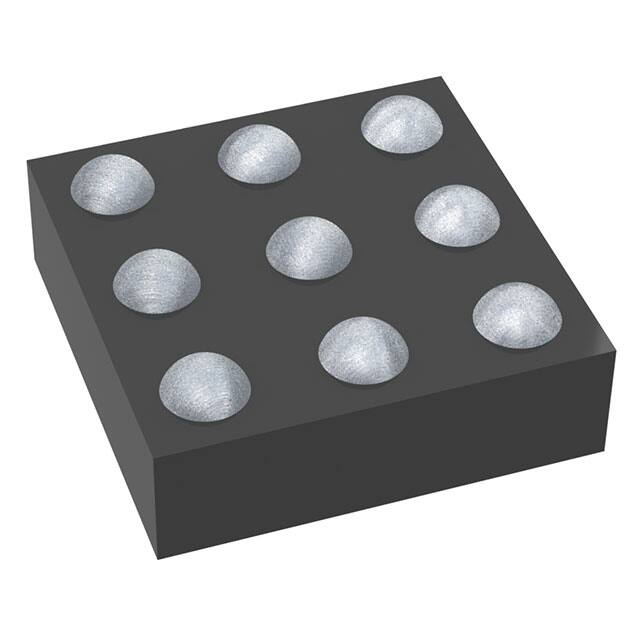
WLCSP9
CASE 567UW
WLCSP9
CASE 567YD
MARKING DIAGRAM
AAA
AYW
AAA = Specific Device Code
A
= Assembly Location
Y
= Year
W = Work Week
(Note: Microdot may be in either location)
Typical Applications
•
•
•
•
Transducer Applications
Sensor Conditioning
Medical Instrumentation
Impedance Sensing
PIN CONNECTIONS
VDD
+INA
+
−INA
−
EN
+INB
+
−INB
−
A
OUTA
A3
OUTB
A2
VDD
A1
OUTA
B3
−INB
B2
EN
B1
−INA
C3
+INB
C2
VSS
C1
+INA
Package Bottom View (Bump Up)
B
OUTB
ORDERING INFORMATION
See detailed ordering, marking and shipping information in the
package dimensions section on page 9 of this data sheet.
VSS
This document contains information on some products that are still under development.
ON Semiconductor reserves the right to change or discontinue these products without
notice.
© Semiconductor Components Industries, LLC, 2020
August, 2020 − Rev. 0
1
Publication Order Number:
NCS20282/D
�NCS20282
Table 1. ABSOLUTE MAXIMUM RATINGS Over operating free−air temperature, unless otherwise stated.
Rating
Unit
7
V
Input Voltage (Note 1)
(VSS – 0.5) to 7
V
Input Current (Note 1)
±5
mA
Output Pin Voltage, Disabled
7
V
Parameter
Supply Voltage (VDD− VSS)
INPUT AND OUTPUT PINS
Output Short Circuit Current (Note 2)
Continuous
TEMPERATURE
Operating Temperature
–40 to +125
°C
Storage Temperature
–65 to +150
°C
Junction Temperature
+150
°C
Human Body Model (HBM)
2000
V
Charged Device Model (CDM)
1000
V
100
mA
ESD RATINGS (Note 3)
OTHER RATINGS
Latch−up Current (Note 4)
MSL
Level 1
Stresses exceeding those listed in the Maximum Ratings table may damage the device. If any of these limits are exceeded, device functionality
should not be assumed, damage may occur and reliability may be affected.
1. The input voltage at any pin may exceed the voltage shown if the current at that pin is limited to 5 mA.
2. Short−circuit to ground.
3. This device series incorporates ESD protection and is tested by the following methods:
ESD Human Body Model tested per JEDEC standard JS−001−2017
ESD Charged Device Model tested per JEDEC standard JS−002−2014
4. Latch−up Current tested per JEDEC standard: JESD78
Table 2. THERMAL INFORMATION
Parameter
Thermal Resistance
Junction to Ambient
NOTE:
Symbol
Cu Area mm2
1.0 oz
2.0 oz
Unit
QJA
10
301
263
°C/W
25
263
230
40
246
215
80
229
204
140
220
196
250
211
188
350
206
183
500
200
179
650
197
175
800
194
173
Four layer JSEC JESD51−7
Table 3. OPERATING CONDITIONS
Parameter
Symbol
Range
Units
Supply Voltage (VDD − VSS)
VS
2.5 to 5.5
V
Specified Operating Temperature Range
TA
−40 to +125
°C
VCM
VSS to VDD
V
Input Common Mode Voltage Range
Functional operation above the stresses listed in the Recommended Operating Ranges is not implied. Extended exposure to stresses beyond
the Recommended Operating Ranges limits may affect device reliability.
www.onsemi.com
2
�NCS20282
Table 4. ELECTRICAL CHARACTERISTICS: VS = 2.5 V to 5.5 V
At TA = +25°C, RL = 10 kW, VCM = VOUT = midsupply, Enable input connected to VDD, unless otherwise noted.
Boldface limits apply over the specified temperature range, TA = –40°C to +125°C, guaranteed by characterization and/or design.
Parameter
Symbol
Conditions
Min
Typ
Max
Units
INPUT CHARACTERISTICS
Offset Voltage
VOS
300
1500
mV
DVOS/DT
2
10
mV/°C
Input Bias Current (Note 5)
IIB
50
800
pA
Input Offset Current
IOS
10
Offset Voltage Drift vs Temp
Input Common−Mode Voltage Range
Common Mode Rejection Ratio
VCM
pA
VSS to VDD
V
86
dB
Differential
10
GW
Common Mode
10
Differential
2
Common Mode
5
CMRR
VCM = −0.1V to (VDD+0.1V)
Input Resistance
RIN
Input Capacitance
CIN
66
pF
OUTPUT CHARACTERISTICS
Open Loop Voltage Gain
Closed Loop Output Impedance
AVOL
0.4 V ≤ VOUT ≤ VDD – 0.4 V
ZOUT_CL
See Figure 23
96
116
dB
See
Figure 23
W
Output Voltage High, Referenced to VDD
VOH
VDD−3
VDD−10
mV
Output Voltage Low, Referenced to VSS
VOL
VSS+6
VSS+10
mV
Short Circuit Current (Note 5)
ISC
Sinking Current
10
15
mA
Sourcing Current
10
15
100
300
Capacitive Load Drive (Note 5)
CL
pF
DYNAMIC PERFORMANCE
Gain Bandwidth Product (Note 5)
GBW
VS = 3 V;
RL = 10 kW, CL = 100 pF
Gain Margin
AM
Phase Margin
Slew Rate
Overload Recovery Time
5.4
7
MHz
CL = 100 pF
50
dB
YM
CL = 100 pF
55
°
SR
AV = +1
5
V/ms
tOR
VIN X AV > VS
1
ms
Voltage Noise Density
eN
fIN = 10 kHz
20
nV/√Hz
Current Noise Density
iN
fIN = 1 Hz
300
fA/√Hz
120
dB
NOISE PERFORMANCE
POWER SUPPLY
PSRR
Power Supply Rejection Ratio
90
Shutdown Enable Time (Notes 5, 6)
tON
30
Shutdown Disable Time (Note 6)
tOFF
30
Shutdown Leakage
Input
VIN = VS+400 mV
Output
VOUT = VS+1 V
Vth(EN)
Operating
Enable Input Leakage Current
IEnable
Enable = + 5.0 V
1.1
Enable = VSS
1.1
Per Channel
No load
500
nA
ms
V
1.3
Disabled
IQ
ms
500
Enable Input Threshold Voltage
Quiescent Current
50
0.5
mA
Quiescent
850
1300
Shutdown
0.3
1
mA
5. Guaranteed by design and/or characterization
6. Shutdown Disable Time (tOFF) and Enable Time (tON) are defined as the time between the 50% point of the signal applied to the EN pin and
the point at which the output voltage reaches the 10% (disable) or 90% (enable) level.
Product parametric performance is indicated in the Electrical Characteristics for the listed test conditions, unless otherwise noted. Product
performance may not be indicated by the Electrical Characteristics if operated under different conditions.
www.onsemi.com
3
�NCS20282
TYPICAL CHARACTERISTICS
Figure 1. CMRR vs. Frequency
Figure 2. PSRR vs. Frequency
Figure 4. Input Bias Current vs.
VCM at VS = 3.3 V
Figure 3. Input Bias Current vs.
VCM at VS = 2.5 V
www.onsemi.com
4
�NCS20282
TYPICAL CHARACTERISTICS
Figure 5. Input Bias Current vs.
VCM at VS = 5.5 V
Figure 6. Input Offset Current vs.
VCM at VS = 2.5 V
Figure 7. Input Offset Current vs.
VCM at VS = 3.3 V
Figure 8. Input Offset Current vs.
VCM at VS = 5.5 V
www.onsemi.com
5
�NCS20282
TYPICAL CHARACTERISTICS
120
160
Phase
140
120
80
40
Gain
60
2.5 V (G)
3.3 V (G)
5.5 V (G)
2.5 V (P)
3.3 V (P)
5.5 V (P)
40
20
0
10
100
20
0
1K
10K
100K
1M
10M
60
15 pF (G)
100 pF (G)
200 pF (G)
300 pF (G)
500 pF (G)
20
−40
0
−60
100M
−20
10
100
−50
0.100
−60
0.075
−20
AV = −10 V/V
RL = 10 KW
10K
−40
100K
1M
10M
−60
100M
0.050
VOLTAGE (V)
−80
−90
−100
−110
AV = +1 V/V
VS = 2.5 V
RL = 10 KW
CL = 15 pF
0.025
0
−0.025
−120
−0.050
VS = 2.5 V
VS = 3.3 V
VS = 5.5 V
−130
10
100
1K
10K
100K
1M
−0.100
−2
10M
0
2
4
6
8
10
FREQUENCY (Hz)
TIME (ms)
Figure 11. Channel Separation
Figure 12. Non Inverting Small Signal
Transient Response
0.100
1.00
0.075
0.75
0.050
0.50
AV = +1 V/V
VS = 5.5 V
RL = 10 KW
0.025
0
−0.025
−0.050
0
2
4
0.25
0
−0.25
Input
CL = 15 pF
CL = 100 pF
−0.75
6
8
10
12
−1.00
−2
0
2
4
6
8
10
TIME (ms)
TIME (ms)
Figure 13. Non Inverting Small Signal
Transient Response
Figure 14. Non Inverting Large Signal
Transient Response
www.onsemi.com
6
12
AV = +1 V/V
VS = 2.5 V
RL = 10 KW
−0.50
Input
CL = 15 pF
CL = 100 pF
−0.075
−0.100
−2
Input
CL = 15 pF
−0.075
VOLTAGE (V)
REJECTION (dB)
20
Figure 10. Open Loop Gain and Phase Margin
vs. CL
−70
VOLTAGE (V)
40
FREQUENCY (Hz)
Figure 9. Open Loop Gain and Phase Margin
vs. Frequency
−140
−150
60
0
1K
FREQUENCY (Hz)
80
15 pF (P)
100 pF (P)
200 pF (P)
300 pF (P)
500 pF (P)
80
40
−20
AV = −10 V/V
RL = 10 KW
CL = 15 pF
100
Gain
100
GAIN (dB)
GAIN (dB)
80
Phase
PHASE MARGIN (°)
140
60
100
−20
100
PHASE MARGIN (°)
120
120
160
12
�NCS20282
3.0
0.100
2.5
2.0
0.075
−1.0
2
4
0.025
0
−0.025
Input
CL = 15 pF
CL = 100 pF
CL = 300 pF
CL = 500 pF
−0.050
Input
CL = 15 pF
CL = 100 pF
0
AV = +1 V/V
VS = 5.5 V
RL = 10 KW
0.050
VOLTAGE (V)
0.5
0
−0.5
−1.5
−2.0
−2.5
−3.0
−2
VOLTAGE (V)
AV = +1 V/V
VS = 5.5 V
RL = 10 KW
1.5
1.0
−0.075
6
8
10
−0.100
−2
12
0
4
6
10
Figure 15. Non Inverting Large Signal
Transient Response
Figure 16. Non Inverting Large Signal
Transient Response vs. CLoad
0.10
0.10
0.08
0.08
0.06
0.06
0.04
Input
CL = 15 pF
CL = 100 pF
0.02
0
AV = −1 V/V
VS = 2.5 V
RL = 10 KW
12
0.04
0.02
Input
CL = 15 pF
CL = 100 pF
0
−0.02
AV = −1 V/V
VS = 5.5 V
RL = 10 KW
−0.04
−0.04
−0.06
−0.06
−0.08
−0.10
−2
−0.08
−0.10
−2
0
2
4
6
8
10
12
0
2
4
6
8
10
TIME (ms)
TIME (ms)
Figure 17. Inverting Small Signal Transient
Response
Figure 18. Inverting Small Signal Transient
Response
12
3
1.00
0.75
2
Input
CL = 15 pF
CL = 100 pF
0.25
AV = −1 V/V
VS = 2.5 V
RL = 10 KW
Input
CL = 15 pF
CL = 100 pF
0
VOLTAGE (V)
0.50
−0.25
1
0
AV = −1 V/V
VS = 5.5 V
RL = 10 KW
−1
−0.50
−2
−0.75
−1.00
−2
8
TIME (ms)
−0.02
VOLTAGE (V)
2
TIME (ms)
VOLTAGE (V)
VOLTAGE (V)
TYPICAL CHARACTERISTICS
0
2
4
6
8
10
−3
−2
12
0
2
4
6
8
10
TIME (ms)
TIME (ms)
Figure 19. Inverting Large Signal Transient
Response
Figure 20. Inverting Large Signal Transient
Response
www.onsemi.com
7
12
�NCS20282
TYPICAL CHARACTERISTICS
3.0
3.0
Enable
Output
2.5
2.5
2.0
VOLTS (V)
VOLTS (V)
2.0
1.5
1.0
0.5
0
0
0
20
10
−0.5
−0.5
40
30
0.5
1.0
FREQUENCY (ms)
Figure 21. Enable Turn−On Time
Figure 22. Disable Turn−Off Time
1.5
10K
NOISE DENSITY (nV/√Hz)
100
10
1
0.1
AV = +1 V/V
10
100
1K
10K
1M
100K
1K
100
10
1
10M
10
1
100
1K
10K
FREQUENCY (Hz)
FREQUENCY (Hz)
Figure 23. Closed Loop Output Impedance
Figure 24. Voltage Noise Density vs.
Frequency
10
VS = 5.5 V
AV = 11 (RTI)
RL = 10 KW
8
6
VOLTAGE (mV)
0.01
0
TIME (ms)
1K
IMPEDANCE (W)
1.0
0.5
−0.5
−10
Enable
Output
1.5
4
2
0
−2
−4
−6
−8
−10
0
1
2
3
4
5
6
7
8
TIME (s)
Figure 25. 0.1 Hz to 10 Hz Noise
www.onsemi.com
8
9
10
100K
�NCS20282
DEVICE ORDERING INFORMATION
Marking
Bump Type
Case Outline
Package
Shipping†
NCS20282FCTTAG
AAA
Sn Plate
567UW
WLCSP−9
(Pb−Free)
5000 / Tape & Reel
NCS20282FCSTAG*
(In Development)
AAA
SAC 405
567YD
WLCSP−9
(Pb−Free)
5000 / Tape & Reel
Device
†For information on tape and reel specifications, including part orientation and tape sizes, please refer to our Tape and Reel Packaging
Specifications Brochure, BRD8011/D.
www.onsemi.com
9
�NCS20282
PACKAGE DIMENSIONS
WLCSP9, 1.02x1.02x0.33
CASE 567UW
ISSUE A
PIN A1
REFERENCE
ÈÈ
ÈÈ
NOTES:
1. DIMENSIONING AND TOLERANCING PER
ASME Y14.5M, 2009.
2. CONTROLLING DIMENSION: MILLIMETERS.
3. COPLANARITY APPLIES TO THE SPHERICAL
CROWNS OF THE SOLDER BALLS.
A B
E
D
DIM
A
A1
A2
b
D
E
e
TOP VIEW
A
0.05 C
0.05 C
A1
SIDE VIEW
NOTE 3
9X
C
SEATING
PLANE
RECOMMENDED
SOLDERING FOOTPRINT*
A1
b
0.03 C A B
A2
MILLIMETERS
MIN
NOM
MAX
−−−
−−−
0.33
0.04
0.06
0.08
0.23 REF
0.180
0.200
0.220
0.99
1.02
1.05
0.99
1.02
1.05
0.35 BSC
e
PACKAGE
OUTLINE
e
C
9X
B
0.20
A
1
2
0.35
PITCH
3
BOTTOM VIEW
0.35
PITCH
DIMENSIONS: MILLIMETERS
*For additional information on our Pb−Free strategy and soldering
details, please download the ON Semiconductor Soldering and
Mounting Techniques Reference Manual, SOLDERRM/D.
www.onsemi.com
10
�NCS20282
PACKAGE DIMENSIONS
WLCSP9, 1.02x1.02x0.441
CASE 567YD
ISSUE O
ON Semiconductor and
are trademarks of Semiconductor Components Industries, LLC dba ON Semiconductor or its subsidiaries in the United States and/or other countries.
ON Semiconductor owns the rights to a number of patents, trademarks, copyrights, trade secrets, and other intellectual property. A listing of ON Semiconductor’s product/patent
coverage may be accessed at www.onsemi.com/site/pdf/Patent−Marking.pdf. ON Semiconductor reserves the right to make changes without further notice to any products herein.
ON Semiconductor makes no warranty, representation or guarantee regarding the suitability of its products for any particular purpose, nor does ON Semiconductor assume any liability
arising out of the application or use of any product or circuit, and specifically disclaims any and all liability, including without limitation special, consequential or incidental damages.
Buyer is responsible for its products and applications using ON Semiconductor products, including compliance with all laws, regulations and safety requirements or standards,
regardless of any support or applications information provided by ON Semiconductor. “Typical” parameters which may be provided in ON Semiconductor data sheets and/or
specifications can and do vary in different applications and actual performance may vary over time. All operating parameters, including “Typicals” must be validated for each customer
application by customer’s technical experts. ON Semiconductor does not convey any license under its patent rights nor the rights of others. ON Semiconductor products are not
designed, intended, or authorized for use as a critical component in life support systems or any FDA Class 3 medical devices or medical devices with a same or similar classification
in a foreign jurisdiction or any devices intended for implantation in the human body. Should Buyer purchase or use ON Semiconductor products for any such unintended or unauthorized
application, Buyer shall indemnify and hold ON Semiconductor and its officers, employees, subsidiaries, affiliates, and distributors harmless against all claims, costs, damages, and
expenses, and reasonable attorney fees arising out of, directly or indirectly, any claim of personal injury or death associated with such unintended or unauthorized use, even if such
claim alleges that ON Semiconductor was negligent regarding the design or manufacture of the part. ON Semiconductor is an Equal Opportunity/Affirmative Action Employer. This
literature is subject to all applicable copyright laws and is not for resale in any manner.
PUBLICATION ORDERING INFORMATION
LITERATURE FULFILLMENT:
Email Requests to: orderlit@onsemi.com
ON Semiconductor Website: www.onsemi.com
◊
TECHNICAL SUPPORT
North American Technical Support:
Voice Mail: 1 800−282−9855 Toll Free USA/Canada
Phone: 011 421 33 790 2910
www.onsemi.com
11
Europe, Middle East and Africa Technical Support:
Phone: 00421 33 790 2910
For additional information, please contact your local Sales Representative
�