NCS2200, NCS2200A,
NCS2202, NCS2202A
Comparators, 0.85 V to 6 V,
10 mA, 1 ms, Rail-to-Rail,
Open Drain and Push-Pull
Outputs
The NCS2200 series is an industry first sub−one volt, low power
comparator family. These devices consume only 10 mA of supply
current. They are guaranteed to operate at a low voltage of 0.85 V
which allows them to be used in systems that require less than 1.0 V
and are fully operational up to 6.0 V which makes them convenient for
use in both 3.0 V and 5.0 V systems. Additional features include no
output phase inversion with overdriven inputs, internal hysteresis,
which allows for clean output switching, and rail−to−rail input and
output performance. The NCS2200 Series is available in
complementary push−pull and open drain outputs and a variety of
packages. There are two industry standard pinouts for SOT−23−5 and
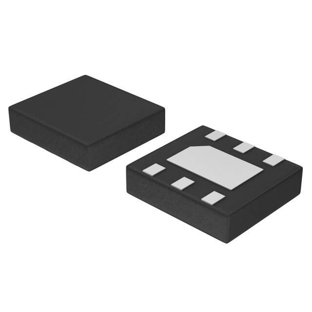
SC70−5 packages. The NCS2200 is also available in the tiny DFN
2x2.2 package. The NCS2200A and NCS2202A are available in a
UDFN 1.2x1.0 package. See package option information in Table 1 on
page 2 for more information.
www.onsemi.com
5
1
SOT−23−5 (TSOP−5)
SN SUFFIX
CASE 483
DFN 2x2.2
SQL SUFFIX
CASE 488
1
6
5
1
SC70−5
SQ SUFFIX
CASE 419A
Features
•
•
•
•
•
•
•
•
•
•
Operating Voltage of 0.85 V to 6.0 V
Rail−to−Rail Input/Output Performance
Low Supply Current of 10 mA
No Phase Inversion with Overdriven Input Signals
Glitchless Transitioning in or out of Tri−State Mode
Complementary or Open Drain Output Configuration
Internal Hysteresis
Propagation Delay of 1.0 ms for NCS2200
NCV Prefix for Automotive and Other Applications Requiring
Unique Site and Control Change Requirements; AEC−Q100
Qualified and PPAP Capable
These Devices are Pb−Free and are RoHS Compliant
UDFN 1.2x1.0
MU SUFFIX
CASE 517AA
1
ORDERING INFORMATION
See detailed ordering and shipping information in the package
dimensions section on page 13 of this data sheet.
DEVICE MARKING INFORMATION
Typical Applications
See general marking information in the device marking
section on page 14 of this data sheet.
• Single Cell NiCd/NiMH Battery Powered Applications
• Automotive
End Products
• Cellphones, Smart Phones
• Alarm and Security Systems
• Personal Digital Assistants
© Semiconductor Components Industries, LLC, 2015
March, 2018 − Rev. 20
1
Publication Order Number:
NCS2200/D
�NCS2200, NCS2200A, NCS2202, NCS2202A
Table 1. COMPARATOR SELECTOR GUIDE
Output Type
Package
Pinout Style
Automotive
Device
N/A
No
NCS2200AMUT1G
N/A
Yes
NCV2200AMUTBG*
No
NCS2200SN1T1G
Yes
NCV2200SN1T1G*
UDFN, 1.2x1.0
1
SOT−23−5
Complementary Push−Pull
2
No
NCS2200SQ2T2G
NCV2200SQ2T2G*
N/A
No
NCS2200SQLT1G
1
No
NCS2202SN1T1G
No
NCS2202SN2T1G
2
DFN, 2x2.2
SOT−23−5
2
SC70−5
UDFN, 1.2 x 1.0
NCS2200SN2T1G
NCV2200SN2T1G*
Yes
SC70−5
Open Drain
No
Yes
Yes
NCV2202SN2T1G*
1
No
NCS2202SQ1T2G
2
No
NCS2202SQ2T2G
N/A
No
NCS2202AMUTBG
*NCV Prefix for Automotive and Other Applications Requiring Unique Site and Control Change Requirements; AEC−Q100 Qualified and PPAP
Capable.
PIN CONNECTIONS
1
Output
2
VCC
Non−Inverting
Input
5
+ -
3
4
Output
1
VEE
Non−Inverting
Input
2
VEE
Inverting
Input
3
5
VCC
4
Inverting
Input
+ -
Style 2 Pinout (SN2T1, SQ2T2)
Style 1 Pinout (SN1T1)
Figure 1. SOT−23−5 (NCS2200, NCS2202), SC70−5 (NCS2200, NCS2202)
VEE
1
6
VOUT
VEE
1
6
VOUT
VCC
2
5
NC
NC
2
5
VCC
IN−
3
4
IN+
IN−
3
4
IN+
Top View
Top View
Figure 2. DFN 2x2.2 (NCS2200)
Figure 3. UDFN 1.2x1.0
(NCS2200A/NCS2202A)
www.onsemi.com
2
�NCS2200, NCS2200A, NCS2202, NCS2202A
MAXIMUM RATINGS
Symbol
Value
Unit
Supply Voltage Range (VCC to VEE)
Rating
VS
6.0
V
Non−inverting/Inverting Input to VEE
VCM
−0.2 to (VCC + 0.2)
V
Operating Junction Temperature
TJ
150
°C
Operating Ambient Temperature Range
NCS2200, NCS2202, NCS2200A, NCS2202A
NCV2200, NCV2202, NCV2200A
TA
Storage Temperature Range
Tstg
−65 to +150
°C
tS
Indefinite
s
Output Short Circuit Duration Time (Note 1)
ESD Tolerance (Note 2)
NCS2200
Human Body Model
Machine Model
NCS2202
Human Body Model
Machine Model
NCS2200A
Human Body Model
Machine Model
NCS2202A
Human Body Model − all pins except output
Human Body Model − output pin
Machine Model
°C
−40 to +105
−40 to +125
ESD
Thermal Resistance, Junction−to−Ambient
TSOP−5
DFN (Note 3)
SC70−5
UDFN
V
HBM
MM
2000
200
HBM
MM
2000
200
HBM
MM
1900
200
HBM
HBM
MM
1500
500
150
RqJA
°C/W
238
215
283
350
Stresses exceeding those listed in the Maximum Ratings table may damage the device. If any of these limits are exceeded, device functionality
should not be assumed, damage may occur and reliability may be affected.
1. The maximum package power dissipation limit must not be exceeded.
TJ(max) * TA
PD +
RqJA
2. ESD data available upon request.
3. For more information, refer to application note, AND8080/D.
www.onsemi.com
3
�NCS2200, NCS2200A, NCS2202, NCS2202A
NCS2200 ELECTRICAL CHARACTERISTICS (For all values VCC = 0.85 V to 6.0 V, VEE = 0 V, TA = 25°C, unless otherwise
noted.) (Note 4)
Symbol
VHYS
VIO
Parameter
Conditions
Min
Typ
Max
Unit
mV
Input Hysteresis
TA = 25°C
2.0
8.0
20
Input Offset Voltage
VCC = 0.85 V
TA = 25°C
TA = TLow to THigh (Note 5)
−10
−12
0.5
−
+10
+12
VCC = 3.0 V
TA = 25°C
TA = TLow to THigh
−6.0
−8.0
0.5
−
+6.0
+8.0
VCC = 6.0 V
TA = 25°C
TA = TLow to THigh
−5.0
−7.0
0.5
−
+5.0
+7.0
−
VEE to VCC
−
VCM
Common Mode Voltage Range
ILEAK
mV
V
Output Leakage Current
VCC = 6.0 V
−
3.3
−
nA
ISC
Output Short−Circuit Sourcing or
Sinking
Vout = GND
−
70
−
mA
CMRR
Common Mode Rejection Ratio
VCM = VCC
53
65
−
dB
−
1.0
−
pA
dB
IIB
PSRR
ICC
VOH
VOL
Input Bias Current
Power Supply Rejection Ratio
DVS = 2.575 V
45
55
−
Supply Current
VCC = 0.85 V
TA = 25°C
TA = TLow to THigh (Note 5)
−
10
−
15
17
VCC = 3.0 V
TA = 25°C
TA = TLow to THigh
−
10
−
15
17
VCC = 6.0 V
TA = 25°C
TA = TLow to THigh
−
10
−
15
17
VCC = 0.85 V, Isource = 0.5 mA
TA = 25°C
TA = TLow to THigh (Note 5)
VCC − 0.2
VCC − 0.225
VCC − 0.10
−
−
VCC = 3.0 V, Isource = 3.0 mA
TA = 25°C
TA = TLow to THigh
VCC − 0.2
VCC − 0.25
VCC − 0.12
−
−
VCC = 6.0 V, Isource = 5.0 mA
TA = 25°C
TA = TLow to THigh
VCC − 0.2
VCC − 0.25
VCC − 0.12
−
−
VCC = 0.85 V, Isink = 0.5 mA
TA = 25°C
TA = TLow to THigh (Note 5)
−
VEE + 0.10
−
VEE + 0.2
VEE + 0.225
VCC = 3.0 V, Isink = 3.0 mA
TA = 25°C
TA = TLow to THigh
−
VEE + 0.12
−
VEE + 0.2
VEE + 0.25
VCC = 6.0 V, Isink = 5.0 mA
TA = 25°C
TA = TLow to THigh
−
VEE + 0.12
−
VEE + 0.2
VEE + 0.25
Output Voltage High
Output Voltage Low
mA
V
V
tPHL
Propagation Delay, High−to−Low
20 mV Overdrive, CL = 15 pF
−
1080
−
ns
tPLH
Propagation Delay, Low−to−High
20 mV Overdrive, CL = 15 pF
−
900
−
ns
tFALL
Output Fall Time
VCC = 6.0 V, CL = 50 pF
−
13
−
ns
tRISE
Output Rise Time
VCC = 6.0 V, CL = 50 pF
−
8.0
−
ns
−
35
−
ms
tPU
Powerup Time
Product parametric performance is indicated in the Electrical Characteristics for the listed test conditions, unless otherwise noted. Product
performance may not be indicated by the Electrical Characteristics if operated under different conditions.
4. The limits over the extended temperature range are guaranteed by design only.
5. NCS2200: TLow = −40°C, THigh = +105°C; NCV2200: TLow = −40°C, THigh = +125°C
www.onsemi.com
4
�NCS2200, NCS2200A, NCS2202, NCS2202A
NCS2202 ELECTRICAL CHARACTERISTICS (For all values VCC = 0.85 V to 6.0 V, VEE = 0 V, TA = 25°C, Rpullup = 10 kW, unless
otherwise noted.) (Note 6)
Symbol
VHYS
VIO
Parameter
Conditions
Min
Typ
Max
Unit
mV
Input Hysteresis
TA = 25°C
2.0
8.0
20
Input Offset Voltage
VCC = 0.85 V
TA = 25°C
TA = TLow to THigh (Note 7)
−10
−12
0.5
−
+10
+12
VCC = 3.0 V
TA = 25°C
TA = TLow to THigh
−6.0
−8.0
0.5
−
+6.0
+8.0
VCC = 6.0 V
TA = 25°C
TA = TLow to THigh
−5.0
−7.0
0.5
−
+5.0
+7.0
−
VEE to VCC
−
VCM
Common Mode Voltage Range
ILEAK
mV
V
Output Leakage Current
VCC = 6.0 V
−
3.3
−
nA
ISC
Output Short−Circuit Sourcing or
Sinking
Vout = GND
−
70
−
mA
CMRR
Common Mode Rejection Ratio
VCM = VCC
53
65
−
dB
−
1.0
−
pA
dB
IIB
PSRR
ICC
VOL
Input Bias Current
Power Supply Rejection Ratio
DVS = 2.575 V
45
55
−
Supply Current
VCC = 0.85 V
TA = 25°C
TA = TLow to THigh (Note 7)
−
10
−
15
17
VCC = 3.0 V
TA = 25°C
TA = TLow to THigh
−
10
−
15
17
VCC = 6.0 V
TA = 25°C
TA = TLow to THigh
−
10
−
15
17
VCC = 0.85 V, Isink = 0.5 mA
TA = 25°C
TA = TLow to THigh (Note 7)
−
VEE + 0.10
−
VEE + 0.2
VEE + 0.225
VCC = 3.0 V, Isink = 3.0 mA
TA = 25°C
TA = TLow to THigh
−
VEE + 0.12
−
VEE + 0.2
VEE + 0.25
VCC = 6.0 V, Isink = 5.0 mA
TA = 25°C
TA = TLow to THigh
−
VEE + 0.12
−
VEE + 0.2
VEE + 0.25
Output Voltage Low
mA
V
tPHL
Propagation Delay, High−to−Low
20 mV Overdrive, CL = 15 pF
−
1000
−
ns
tPLH
Propagation Delay, Low−to−High
20 mV Overdrive, CL = 15 pF
−
800
−
ns
tFALL
Output Fall Time
VCC = 6.0 V, CL = 50 pF
−
6.0
−
ns
tRISE
Output Rise Time
VCC = 6.0 V, CL = 50 pF
−
260
−
ns
−
35
−
ms
tPU
Powerup Time
Product parametric performance is indicated in the Electrical Characteristics for the listed test conditions, unless otherwise noted. Product
performance may not be indicated by the Electrical Characteristics if operated under different conditions.
6. The limits over the extended temperature range are guaranteed by design only.
7. NCS2202: TLow = −40°C, THigh = +105°C; NCV2202: TLow = −40°C, THigh = +125°C
www.onsemi.com
5
�NCS2200, NCS2200A, NCS2202, NCS2202A
NCS2200A ELECTRICAL CHARACTERISTICS (For all values VCC = 0.85 V to 6.0 V, VEE = 0 V, TA = 25°C, unless otherwise
noted.) (Note 8)
Symbol
VHYS
VIO
Parameter
Input Hysteresis
Input Offset Voltage
VCM
ISC
Common Mode Voltage Range
Output Short−Circuit Sourcing or
Sinking
CMRR
IIB
PSRR
Common Mode Rejection Ratio
Input Bias Current
Power Supply Rejection Ratio
ICC
VOH
VOL
tPHL
tPLH
tFALL
tRISE
Supply Current
Output Voltage High
Output Voltage Low
Propagation Delay, High−to−Low
Propagation Delay, Low−to−High
Output Fall Time
Output Rise Time
Conditions
TA = 25°C
VCC = 0.85 V
TA = 25°C
TA = TLOW to THIGH
VCC = 3.0 V
TA = 25°C
TA = TLOW to THIGH
VCC = 6.0 V
TA = 25°C
TA = TLOW to THIGH
Vout = GND
VCM = VCC
DVS = 2.575 V
VCC = 0.85 V
TA = 25°C
TA = TLOW to THIGH
VCC = 3.0 V
TA = 25°C
TA = TLOW to THIGH
VCC = 6.0 V
TA = 25°C
TA = TLOW to THIGH
VCC = 0.85 V, Isource = 0.5 mA
TA = 25°C
TA = TLOW to THIGH
VCC = 3.0 V, Isource = 3.0 mA
TA = 25°C
TA = TLOW to THIGH
VCC = 6.0 V, Isource = 5.0 mA
TA = 25°C
TA = TLOW to THIGH
VCC = 0.85 V, Isink = 0.5 mA
TA = 25°C
TA = TLOW to THIGH
VCC = 3.0 V, Isink = 3.0 mA
TA = 25°C
TA = TLOW to THIGH
VCC = 6.0 V, Isink = 5.0 mA
TA = 25°C
TA = TLOW to THIGH
20 mV Overdrive, CL = 15 pF,
VCC = 2.85 V
VCC = 6.0 V, CL = 50 pF (Note 9)
VCC = 6.0 V, CL = 50 pF (Note 9)
Min
Typ
Max
Unit
2.0
4.5
20
mV
−10
−12
0.5
−
+10
+12
−6.0
−8.0
0.5
−
+6.0
+8.0
−5.0
−7.0
−
−
0.5
−
VEE to VCC
60
+5.0
+7.0
−
−
V
mA
53
−
45
70
1.0
80
−
−
−
dB
pA
dB
−
7.5
−
15
17
−
8.0
−
15
17
−
9.0
−
15
17
VCC − 0.25
VCC − 0.275
VCC − 0.10
−
−
VCC − 0.3
VCC − 0.35
VCC − 0.12
−
−
VCC − 0.3
VCC − 0.35
VCC − 0.12
−
−
−
VEE + 0.10
−
VEE + 0.25
VEE + 0.275
−
VEE + 0.12
−
VEE + 0.3
VEE + 0.35
−
VEE + 0.12
−
625
750
22
20
VEE + 0.3
VEE + 0.35
−
−
−
−
mV
mA
V
V
−
−
−
−
ns
ns
ns
ns
Product parametric performance is indicated in the Electrical Characteristics for the listed test conditions, unless otherwise noted. Product
performance may not be indicated by the Electrical Characteristics if operated under different conditions.
8. The limits over the extended temperature range are guaranteed by design only.
9. Input signal: 1 kHz, squarewave signal with 10 ns edge rate.
10. NCS2200A: TLOW = −40°C, THIGH = +105°C; NCV2200A: TLOW = −40°C, THIGH = +125°C.
www.onsemi.com
6
�NCS2200, NCS2200A, NCS2202, NCS2202A
NCS2202A ELECTRICAL CHARACTERISTICS (For all values VCC = 0.85 V to 6.0 V, VEE = 0 V, TA = 25°C, Rpullup = 10 kW,
unless otherwise noted.) (Note 11)
Symbol
VHYS
VIO
Parameter
Input Hysteresis
Input Offset Voltage
VCM
ISC
Common Mode Voltage Range
Output Short−Circuit Sourcing or
Sinking
CMRR
IIB
PSRR
Common Mode Rejection Ratio
Input Bias Current
Power Supply Rejection Ratio
ICC
VOL
tPHL
tPLH
Supply Current
Output Voltage Low
Propagation Delay − High to Low
Propagation Delay − Low to High
Conditions
Min
Typ
Max
Unit
TA = 25°C
VCC = 0.85 V
TA = 25°C
TA = −40°C to 105°C
VCC = 3.0 V
TA = 25°C
TA = −40°C to 105°C
VCC = 6.0 V
TA = 25°C
TA = −40°C to 105°C
2.0
4.5
20
mV
−10
−12
0.3
−
+10
+12
−6.0
−8.0
0.4
−
+6.0
+8.0
−5.0
−7.0
−
−
0.4
−
VEE to VCC
60
+5.0
+7.0
−
−
V
mA
53
−
45
80
1.0
80
−
−
−
dB
pA
dB
−
7.5
−
15
17
−
8.0
−
15
17
−
9.0
−
15
17
−
VEE + 0.14
−
VEE + 0.25
VEE + 0.275
−
VEE + 0.18
−
VEE + 0.3
VEE + 0.35
−
−
VEE + 0.20
−
580
VEE + 0.3
VEE + 0.35
−
50 mV Overdrive, CL = 15 pF,
VCC = 2.85 V
−
350
−
100 mV Overdrive, CL = 15 pF,
VCC = 2.85 V
−
220
−
20 mV Overdrive, CL = 15 pF,
VCC = 2.85 V
−
550
−
50 mV Overdrive, CL = 15 pF,
VCC = 2.85 V
−
400
−
100 mV Overdrive, CL = 15 pF,
VCC = 2.85 V
−
340
−
Vout = GND
VCM = VCC
DVS = 2.575 V
VCC = 0.85 V
TA = 25°C
TA = −40°C to 105°C
VCC = 3.0 V
TA = 25°C
TA = −40°C to 105°C
VCC = 6.0 V
TA = 25°C
TA = −40°C to 105°C
VCC = 0.85 V, Isink = 0.5 mA
TA = 25°C
TA = −40°C to 105°C
VCC = 3.0 V, Isink = 3.0 mA
TA = 25°C
TA = −40°C to 105°C
VCC = 6.0 V, Isink = 5.0 mA
TA = 25°C
TA = −40°C to 105°C
20 mV Overdrive, CL = 15 pF,
VCC = 2.85 V
mV
mA
V
ns
ns
tFALL
Output Fall Time
VCC = 6.0 V, CL = 50 pF (Note
12)
−
5.0
−
ns
tRISE
Output Rise Time
VCC = 6.0 V, CL = 50 pF (Note
12)
−
235
−
ns
Product parametric performance is indicated in the Electrical Characteristics for the listed test conditions, unless otherwise noted. Product
performance may not be indicated by the Electrical Characteristics if operated under different conditions.
11. The limits over the extended temperature range are guaranteed by design only.
12. Input signal: 1 kHz, squarewave signal with 10 ns edge rate.
www.onsemi.com
7
�NCS2200, NCS2200A, NCS2202, NCS2202A
1000
TA = 25°C
VCC = 5.0 V
ICC, SUPPLY CURRENT (mA)
ICC, SUPPLY CURRENT (mA)
12
11
10
9.0
8.0
7.0
6.0
−50
0
−25
25
50
75
VCC = 2.7 V
0.1
10
1.0
100
TA, AMBIENT TEMPERATURE (°C)
FREQUENCY (kHz)
Figure 1. NCS2200 Series Supply Current
versus Temperature
Figure 2. NCS2200 Series Supply Current
versus Output Transition Frequency
300
1000
VCC − VOH, OUTPUT VOLTAGE
HIGH STATE (mV)
ICC, SUPPLY CURRENT (mA)
VCC = 5.0 V
10
1.0
0.01
100
12
10
8.0
6.0
4.0
TA = 85°C
TA = 25°C
2.0
TA = −40°C
0
2.0
1.0
3.0
4.0
5.0
100
10
1.0
0.1
1.0
10
VCC, SUPPLY VOLTAGE (V)
Isource, OUTPUT SOURCE CURRENT (mA)
Figure 3. NCS2200 Series Supply Current
versus Supply Voltage
Figure 4. NCS2200 Output Voltage
High State versus Output Source Current
1000
VCC = 5.0 V
TA = 25°C
100
10
1.0
0.1
0.01
VCC = 5.0 V
TA = 25°C
0.1
0.01
6.0
VOL, OUTPUT VOLTAGE LOW STATE (mV)
0
VOL, OUTPUT VOLTAGE LOW STATE (mV)
100
0.1
1.0
10
160
140
VCC = 5.0 V
ILOAD = 4.0 mA
120
100
80
60
40
20
0
−100
−50
0
50
100
Isink, OUTPUT SINK CURRENT, (mA)
TA, AMBIENT TEMPERATURE (°C)
Figure 5. NCS2200 Series Output Voltage
Low State versus Output Sink Current
Figure 6. NCS2200 Series Output Voltage
Low State versus Temperature
www.onsemi.com
8
150
�1.0
4.95
VCC = 5.0 V
ILOAD = 4.0 mA
4.94
PROPAGATION DELAY (ms)
VOH, OUTPUT VOLTAGE HIGH STATE (mV)
NCS2200, NCS2200A, NCS2202, NCS2202A
4.93
4.92
4.91
4.90
4.89
4.88
−100
−50
0
50
100
0.8
tPLH
0.6
tPHL
0.4
0.2
VCC = 5.0 V
Input Overdrive = 50 mV
0
−50
150
Figure 7. NCS2200 Series Output Voltage
High State versus Temperature
25
50
75
600
tLH
500
400
tHL
300
200
TA = 25°C
Input Overdrive = 100 mV
100
VCC = 2.7 V
TA = 25°C
1.0
0.8
0.6
tPLH
0.4
tPHL
0.2
0
0
1.0
2.0
3.0
4.0
5.0
6.0
0
50
VCC, SUPPLY VOLTAGE (V)
100
150
Figure 10. NCS2200 Series Propagation Delay
versus Input Overdrive
0.8
VCC = 5.0 V
TA = 25°C
0.7
tPLH
0.6
VCC
2 V/Div
0.5
0.4
0.3
tPHL
Output
0.2
0.1
Input Overdrive = 50 mV
0
0
50
100
200
INPUT OVERDRIVE (mV)
Figure 9. NCS2200 Series Output Response
Time versus Supply Voltage
PROPAGATION DELAY (ms)
100
1.2
PROPAGATION DELAY (ms)
OUTPUT RESPONSE TIME (ns)
0
Figure 8. NCS2200 Series Propagation Delay
versus Temperature
700
0
−25
TA, AMBIENT TEMPERATURE (°C)
TA, AMBIENT TEMPERATURE (°C)
150
200
INPUT OVERDRIVE (mV)
10 ms/Div
Figure 12. NCS2200 Series Powerup Delay
Figure 11. NCS2200 Series Propagation Delay
versus Input Overdrive
www.onsemi.com
9
�3.0
TA = 25°C
2.0
1.0
0
−1.0
−2.0
−3.0
1.0
2.0
3.0
5.0
4.0
6.0
ILEAK, OUTPUT LEAKAGE CURRENT (nA)
VCM, INPUT COMMON MODE VOLTAGE RANGE (V)
NCS2200, NCS2200A, NCS2202, NCS2202A
180
160
140
120
100
TA = 85°C
80
60
40
TA = 25°C
20
TA = −40°C
0
0
1.0
2.0
VS, SUPPLY VOLTAGE (V)
3.0
Figure 13. NCS2200 Series Input Common
Mode Voltage Range versus Supply Voltage
INPUT BIAS CURRENT (pA)
3500
2500
1500
500
−500
−20
5.0
6.0
7.0
Figure 14. NCS2202 Output Leakage Current
versus Output Voltage
4500
−40
4.0
VOUT, OUTPUT VOLTAGE (V)
0
20
40
60
80
100
TEMPERATURE (°C)
Figure 15. Input Bias Current versus
Temperature
www.onsemi.com
10
120
8.0
�NCS2200, NCS2200A, NCS2202, NCS2202A
OPERATING DESCRIPTION
The NCS2200 series is an industry first sub−one volt, low
power comparator family. This series is designed for
rail−to−rail input and output performance. These devices
consume only 10 mA of supply current while achieving a
typical propagation delay of 1.1 ms at a 20 mV input
overdrive. Figures 10 and 11 show propagation delay with
various input overdrives. This comparator family is
guaranteed to operate at a low voltage of 0.85 V up to 6.0 V.
This is accomplished by the use of a modified analog CMOS
process that implements depletion MOSFET devices. The
common−mode input voltage range extends 0.1 V beyond
the upper and lower rail without phase inversion or other
adverse effects. This series is available in the SOT−23−5
package. Additionally, the NCS2200 device is available in
the tiny DFN 2x2.2 package and the SC70−5 package.
NCS2200A is available in UDFN package.
Output Stage
The NCS2200 has a complementary P and N Channel
output stage that has capability of driving a rail−to−rail
output swing with a load ranging up to 5.0 mA. It is designed
such that shoot−through current is minimized while
switching. This feature eliminates the need for bypass
capacitors under most circumstances.
The NCS2202 has an open drain N−channel output stage
that can be pulled up to 6.0 V (max) with an external resistor.
This facilitates mixed voltage system applications.
VCC
VCC
IN (+)
IN (+)
Output
Output
IN (−)
IN (−)
VEE
VEE
Figure 16. NCS2200/NCS2200A
Complementary Push−Pull Output
Configuration
Figure 17. NCS2202/NCS2202A Open Drain
Output Configuration
VCC
Rx
Cx
IN (−)
NCS
2200
IN (+)
VO
OUT
R2
R1
The oscillation frequency can be programmed as follows:
1
f+1+
T
2.2 RxCx
Figure 18. Schmitt Trigger Oscillator
www.onsemi.com
11
�NCS2200, NCS2200A, NCS2202, NCS2202A
VCC
1 MW
R1
100 pF
t0
R2
1 MW
IN (−)
NCS
2200
IN (+)
VCC
VO
OUT
t0
C1
R3
The resistor divider R1 and R2 can be used to
set the magnitude of the input pulse. The pulse
width is set by adjusting C1 and R3.
Figure 19. One−Shot Multivibrator
+5 V
+3 V
100 kW
R pullup
IN (−)
NCS
2202
IN (+)
100 kW
+3 V Logic Output
OUT
+5 V Logic Input
This circuit converts 5 V logic to 3 V logic. Using the
NCS2202/A allows for full 5 V logic swing without creating
overvoltage on the 3 V logic input.
Figure 20. Logic Level Translator
VCC
IN (−)
NCS
2200
IN (+)
OUT
100 mV
Figure 21. Zero−Crossing Detector
www.onsemi.com
12
t1
0
�NCS2200, NCS2200A, NCS2202, NCS2202A
ORDERING INFORMATION
Pinout Style
Output Type
Package
Shipping†
NCS2200AMUT1G
N/A
Complementary Push−Pull
UDFN
(Pb−Free)
3000 / Tape & Reel
NCV2200AMUTBG*
N/A
Complementary Push−Pull
UDFN
(Pb−Free)
3000 / Tape & Reel
NCS2200SN1T1G
1
Complementary Push−Pull
SOT−23−5 (TSOP−5)
(Pb−Free)
3000 / Tape & Reel
NCV2200SN1T1G*
1
Complementary Push−Pull
SOT−23−5 (TSOP−5)
(Pb−Free)
3000 / Tape & Reel
NCS2200SN2T1G
2
Complementary Push−Pull
SOT−23−5 (TSOP−5)
(Pb−Free)
3000 / Tape & Reel
NCV2200SN2T1G*
2
Complementary Push−Pull
SOT−23−5 (TSOP−5)
(Pb−Free)
3000 / Tape & Reel
NCS2200SQ2T2G
2
Complementary Push−Pull
SC70−5
(Pb−Free)
3000 / Tape & Reel
NCV2200SQ2T2G*
2
Complementary Push−Pull
SC70−5
(Pb−Free)
3000 / Tape & Reel
NCS2200SQLT1G
N/A
Complementary Push−Pull
DFN, 2x2.2
(Pb−Free)
3000 / Tape & Reel
NCS2202SN1T1G
1
Open Drain
SOT−23−5 (TSOP−5)
(Pb−Free)
3000 / Tape & Reel
NCS2202SN2T1G
2
Open Drain
SOT−23−5 (TSOP−5)
(Pb−Free)
3000 / Tape & Reel
NCV2202SN2T1G*
2
Open Drain
SOT−23−5 (TSOP−5)
(Pb−Free)
3000 / Tape & Reel
NCS2202SQ1T2G
1
Open Drain
SC70−5
(Pb−Free)
3000 / Tape & Reel
NCS2202SQ2T2G
2
Open Drain
SC70−5
(Pb−Free)
3000 / Tape & Reel
NCS2202AMUTBG
N/A
Open Drain
UDFN
(Pb−Free)
3000 / Tape & Reel
Device
This device contains 93 active transistors.
†For information on tape and reel specifications, including part orientation and tape sizes, please refer to our Tape and Reel Packaging
Specifications Brochure, BRD8011/D.
*NCV Prefix for Automotive and Other Applications Requiring Unique Site and Control Change Requirements; AEC−Q100 Qualified and
PPAP Capable.
www.onsemi.com
13
�NCS2200, NCS2200A, NCS2202, NCS2202A
MARKING DIAGRAMS
SOT−23−5
(TSOP−5)
SN SUFFIX
CASE 483
SC70−5
SQ SUFFIX
CASE 419A
5
5
CBx MG
G
CAx AYWG
G
1
1
x = I for NCS2200SN1T1
J for NCS2200SN2T1
M for NCS2202SN1T1
N for NCS2202SN2T1
A = Assembly Location
Y = Year
W = Work Week
G = Pb−Free Package
CBx
x
= Specific Device Code
= A for NCS2200SQ2T2
D for NCS2202SQ1T2G
E for NCS2202SQ2T2G
M
= Date Code*
G
= Pb−Free Package
(Note: Microdot may be in either location)
*Date Code orientation, position, and underbar
may vary depending upon manufacturing location.
(Note: Microdot may be in either location)
DFN6 2x2.2
SQL SUFFIX
CASE 488
UDFN6 1.2x1.0
MU SUFFIX
CASE 517AA
1
CB MG
G
1
xM
G
(Top View)
x
CB = Specific Device Code
M = Date Code*
G
= Pb−Free Package
M
G
(Note: Microdot may be in either location)
*Date Code overbar and underbar may vary
depending upon manufacturing location.
www.onsemi.com
14
S for Specific Device Code
V for NCS2202A (V with 180° Rotation)
= Date Code
= Pb−Free Package
�MECHANICAL CASE OUTLINE
PACKAGE DIMENSIONS
SC−88A (SC−70−5/SOT−353)
CASE 419A−02
ISSUE L
SCALE 2:1
A
NOTES:
1. DIMENSIONING AND TOLERANCING
PER ANSI Y14.5M, 1982.
2. CONTROLLING DIMENSION: INCH.
3. 419A−01 OBSOLETE. NEW STANDARD
419A−02.
4. DIMENSIONS A AND B DO NOT INCLUDE
MOLD FLASH, PROTRUSIONS, OR GATE
BURRS.
G
5
4
−B−
S
1
2
DATE 17 JAN 2013
DIM
A
B
C
D
G
H
J
K
N
S
3
D 5 PL
0.2 (0.008)
B
M
M
N
INCHES
MIN
MAX
0.071
0.087
0.045
0.053
0.031
0.043
0.004
0.012
0.026 BSC
--0.004
0.004
0.010
0.004
0.012
0.008 REF
0.079
0.087
MILLIMETERS
MIN
MAX
1.80
2.20
1.15
1.35
0.80
1.10
0.10
0.30
0.65 BSC
--0.10
0.10
0.25
0.10
0.30
0.20 REF
2.00
2.20
J
GENERIC MARKING
DIAGRAM*
C
K
H
XXXMG
G
SOLDER FOOTPRINT
0.50
0.0197
XXX = Specific Device Code
M
= Date Code
G
= Pb−Free Package
0.65
0.025
0.65
0.025
0.40
0.0157
1.9
0.0748
SCALE 20:1
(Note: Microdot may be in either location)
*This information is generic. Please refer to
device data sheet for actual part marking.
Pb−Free indicator, “G” or microdot “G”, may
or may not be present. Some products may
not follow the Generic Marking.
mm Ǔ
ǒinches
STYLE 1:
PIN 1. BASE
2. EMITTER
3. BASE
4. COLLECTOR
5. COLLECTOR
STYLE 2:
PIN 1. ANODE
2. EMITTER
3. BASE
4. COLLECTOR
5. CATHODE
STYLE 3:
PIN 1. ANODE 1
2. N/C
3. ANODE 2
4. CATHODE 2
5. CATHODE 1
STYLE 4:
PIN 1. SOURCE 1
2. DRAIN 1/2
3. SOURCE 1
4. GATE 1
5. GATE 2
STYLE 6:
PIN 1. EMITTER 2
2. BASE 2
3. EMITTER 1
4. COLLECTOR
5. COLLECTOR 2/BASE 1
STYLE 7:
PIN 1. BASE
2. EMITTER
3. BASE
4. COLLECTOR
5. COLLECTOR
STYLE 8:
PIN 1. CATHODE
2. COLLECTOR
3. N/C
4. BASE
5. EMITTER
STYLE 9:
PIN 1. ANODE
2. CATHODE
3. ANODE
4. ANODE
5. ANODE
DOCUMENT NUMBER:
DESCRIPTION:
98ASB42984B
STYLE 5:
PIN 1. CATHODE
2. COMMON ANODE
3. CATHODE 2
4. CATHODE 3
5. CATHODE 4
Note: Please refer to datasheet for
style callout. If style type is not called
out in the datasheet refer to the device
datasheet pinout or pin assignment.
Electronic versions are uncontrolled except when accessed directly from the Document Repository.
Printed versions are uncontrolled except when stamped “CONTROLLED COPY” in red.
SC−88A (SC−70−5/SOT−353)
PAGE 1 OF 1
ON Semiconductor and
are trademarks of Semiconductor Components Industries, LLC dba ON Semiconductor or its subsidiaries in the United States and/or other countries.
ON Semiconductor reserves the right to make changes without further notice to any products herein. ON Semiconductor makes no warranty, representation or guarantee regarding
the suitability of its products for any particular purpose, nor does ON Semiconductor assume any liability arising out of the application or use of any product or circuit, and specifically
disclaims any and all liability, including without limitation special, consequential or incidental damages. ON Semiconductor does not convey any license under its patent rights nor the
rights of others.
© Semiconductor Components Industries, LLC, 2018
www.onsemi.com
�MECHANICAL CASE OUTLINE
PACKAGE DIMENSIONS
TSOP−5
CASE 483
ISSUE N
5
1
SCALE 2:1
NOTES:
1. DIMENSIONING AND TOLERANCING PER ASME
Y14.5M, 1994.
2. CONTROLLING DIMENSION: MILLIMETERS.
3. MAXIMUM LEAD THICKNESS INCLUDES LEAD FINISH
THICKNESS. MINIMUM LEAD THICKNESS IS THE
MINIMUM THICKNESS OF BASE MATERIAL.
4. DIMENSIONS A AND B DO NOT INCLUDE MOLD
FLASH, PROTRUSIONS, OR GATE BURRS. MOLD
FLASH, PROTRUSIONS, OR GATE BURRS SHALL NOT
EXCEED 0.15 PER SIDE. DIMENSION A.
5. OPTIONAL CONSTRUCTION: AN ADDITIONAL
TRIMMED LEAD IS ALLOWED IN THIS LOCATION.
TRIMMED LEAD NOT TO EXTEND MORE THAN 0.2
FROM BODY.
D 5X
NOTE 5
2X
DATE 12 AUG 2020
0.20 C A B
0.10 T
M
2X
0.20 T
5
B
1
4
2
B
S
3
K
DETAIL Z
G
A
A
TOP VIEW
DIM
A
B
C
D
G
H
J
K
M
S
DETAIL Z
J
C
0.05
H
C
SIDE VIEW
SEATING
PLANE
END VIEW
GENERIC
MARKING DIAGRAM*
SOLDERING FOOTPRINT*
0.95
0.037
MILLIMETERS
MIN
MAX
2.85
3.15
1.35
1.65
0.90
1.10
0.25
0.50
0.95 BSC
0.01
0.10
0.10
0.26
0.20
0.60
0_
10 _
2.50
3.00
1.9
0.074
5
5
XXXAYWG
G
1
1
Analog
2.4
0.094
XXX = Specific Device Code
A
= Assembly Location
Y
= Year
W = Work Week
G
= Pb−Free Package
1.0
0.039
XXX MG
G
Discrete/Logic
XXX = Specific Device Code
M = Date Code
G
= Pb−Free Package
(Note: Microdot may be in either location)
0.7
0.028
SCALE 10:1
mm Ǔ
ǒinches
*For additional information on our Pb−Free strategy and soldering
details, please download the ON Semiconductor Soldering and
Mounting Techniques Reference Manual, SOLDERRM/D.
DOCUMENT NUMBER:
DESCRIPTION:
98ARB18753C
TSOP−5
*This information is generic. Please refer to
device data sheet for actual part marking.
Pb−Free indicator, “G” or microdot “ G”,
may or may not be present.
Electronic versions are uncontrolled except when accessed directly from the Document Repository.
Printed versions are uncontrolled except when stamped “CONTROLLED COPY” in red.
PAGE 1 OF 1
ON Semiconductor and
are trademarks of Semiconductor Components Industries, LLC dba ON Semiconductor or its subsidiaries in the United States and/or other countries.
ON Semiconductor reserves the right to make changes without further notice to any products herein. ON Semiconductor makes no warranty, representation or guarantee regarding
the suitability of its products for any particular purpose, nor does ON Semiconductor assume any liability arising out of the application or use of any product or circuit, and specifically
disclaims any and all liability, including without limitation special, consequential or incidental damages. ON Semiconductor does not convey any license under its patent rights nor the
rights of others.
© Semiconductor Components Industries, LLC, 2018
www.onsemi.com
�MECHANICAL CASE OUTLINE
PACKAGE DIMENSIONS
DFN6 2x2.2 mm
CASE 488−03
ISSUE G
DATE 06 FEB 2006
SCALE 4:1
D
NOTES:
1. DIMENSIONING AND TOLERANCING PER
ASME Y14.5M, 1994.
2. CONTROLLING DIMENSION: MILLIMETERS.
3. DIMENSION b APPLIES TO PLATED
TERMINAL AND IS MEASURED BETWEEN
0.25 AND 0.30mm FROM TERMINAL.
4. COPLANARITY APPLIES TO THE EXPOSED
PAD AS WELL AS THE TERMINALS.
5. TERMINAL b MAY HAVE MOLD COMPOUND
MATERIAL ALONG SIDE EDGE.
6. DETAILS A AND B SHOW OPTIONAL VIEWS
FOR END OF TERMINAL LEAD AT EDGE OF
PACKAGE AND SIDE EDGE OF PACKAGE.
B
A
ÍÍÍ
ÍÍÍ
ÍÍÍ
E
PIN ONE
REFERENCE
0.10 C
2X
DIM
A
A1
A3
b
b1
D
D2
E
e
L
L1
TOP VIEW
2X
0.10 C
A3
DETAIL B
0.10 C
A
6X
0.08 C
A1
SIDE VIEW
0.10 C A
0.05 C
C
B b1
0.20
0.30
0.40
0.30
0.00
MILLIMETERS
NOM
MAX
0.90
1.00
0.03
0.05
0.20 REF
0.25
0.30
0.35
0.40
2.00 BSC
0.50
0.60
2.20 BSC
0.65 BSC
0.35
0.40
0.05
0.10
GENERIC
MARKING DIAGRAM*
e
3
1
NOTE 3
SEATING
PLANE
MIN
0.80
0.00
xxM
DETAIL A
D2
xx
M
4
6
6X
L
b
*This information is generic. Please refer
to device data sheet for actual part
marking.
5X
0.10 C A
0.05 C
BOTTOM VIEW
EDGE OF PACKAGE
MOLD CMPD
L1
A1
DETAIL A
Bottom View
(Optional)
ÉÉ
ÉÉ
= Specific Device Code
= Date Code
B
SOLDERING FOOTPRINT*
NOTE 3
0.50
0.020
EXPOSED Cu
DETAIL B
Side View
(Optional)
A3
0.65
0.025
0.40
0.016
0.50
0.020
1.9
0.075
0.65
0.025
SCALE 10:1
*For additional information on our Pb−Free strategy and soldering
details, please download the ON Semiconductor Soldering and
Mounting Techniques Reference Manual, SOLDERRM/D.
DOCUMENT NUMBER:
DESCRIPTION:
98AON04199D
DFN6 2 X 2.2 X 0.9 X 0.65P
Electronic versions are uncontrolled except when accessed directly from the Document Repository.
Printed versions are uncontrolled except when stamped “CONTROLLED COPY” in red.
PAGE 1 OF 1
ON Semiconductor and
are trademarks of Semiconductor Components Industries, LLC dba ON Semiconductor or its subsidiaries in the United States and/or other countries.
ON Semiconductor reserves the right to make changes without further notice to any products herein. ON Semiconductor makes no warranty, representation or guarantee regarding
the suitability of its products for any particular purpose, nor does ON Semiconductor assume any liability arising out of the application or use of any product or circuit, and specifically
disclaims any and all liability, including without limitation special, consequential or incidental damages. ON Semiconductor does not convey any license under its patent rights nor the
rights of others.
© Semiconductor Components Industries, LLC, 2019
www.onsemi.com
�MECHANICAL CASE OUTLINE
PACKAGE DIMENSIONS
UDFN6, 1.2x1.0, 0.4P
CASE 517AA−01
ISSUE D
1
SCALE 8:1
EDGE OF PACKAGE
2X
0.10 C
ÉÉ
ÉÉ
ÉÉ
L1
E
DETAIL A
Bottom View
(Optional)
TOP VIEW
2X
EXPOSED Cu
0.10 C
(A3)
0.10 C
A1
A
10X
0.08 C
ÉÉÉ
ÉÉÉ
A3
DETAIL B
Side View
(Optional)
5X
XM
L
3
X
M
L2
b
0.10 C A B
0.05 C
6
= Specific Device Code
= Date Code
*This information is generic. Please refer to
device data sheet for actual part marking.
Pb−Free indicator, “G” or microdot “ G”,
may or may not be present.
4
e
NOTE 3
MILLIMETERS
MIN
MAX
0.45
0.55
0.00
0.05
0.127 REF
0.15
0.25
1.20 BSC
1.00 BSC
0.40 BSC
0.30
0.40
0.00
0.15
0.40
0.50
GENERIC
MARKING DIAGRAM*
C
A1
6X
DIM
A
A1
A3
b
D
E
e
L
L1
L2
MOLD CMPD
SEATING
PLANE
SIDE VIEW
1
NOTES:
1. DIMENSIONING AND TOLERANCING PER
ASME Y14.5M, 1994.
2. CONTROLLING DIMENSION: MILLIMETERS.
3. DIMENSION b APPLIES TO PLATED TERMINAL
AND IS MEASURED BETWEEN 0.25 AND
0.30 mm FROM TERMINAL.
4. COPLANARITY APPLIES TO THE EXPOSED
PAD AS WELL AS THE TERMINALS.
A
B
D
PIN ONE
REFERENCE
DATE 03 SEP 2010
MOUNTING FOOTPRINT*
BOTTOM VIEW
6X
6X
0.42
0.40
PITCH
0.22
1.07
DIMENSIONS: MILLIMETERS
*For additional information on our Pb−Free strategy and soldering
details, please download the ON Semiconductor Soldering and
Mounting Techniques Reference Manual, SOLDERRM/D.
DOCUMENT NUMBER:
DESCRIPTION:
98AON22068D
6 PIN UDFN, 1.2X1.0, 0.4P
Electronic versions are uncontrolled except when accessed directly from the Document Repository.
Printed versions are uncontrolled except when stamped “CONTROLLED COPY” in red.
PAGE 1 OF 1
ON Semiconductor and
are trademarks of Semiconductor Components Industries, LLC dba ON Semiconductor or its subsidiaries in the United States and/or other countries.
ON Semiconductor reserves the right to make changes without further notice to any products herein. ON Semiconductor makes no warranty, representation or guarantee regarding
the suitability of its products for any particular purpose, nor does ON Semiconductor assume any liability arising out of the application or use of any product or circuit, and specifically
disclaims any and all liability, including without limitation special, consequential or incidental damages. ON Semiconductor does not convey any license under its patent rights nor the
rights of others.
© Semiconductor Components Industries, LLC, 2019
www.onsemi.com
�onsemi,
, and other names, marks, and brands are registered and/or common law trademarks of Semiconductor Components Industries, LLC dba “onsemi” or its affiliates
and/or subsidiaries in the United States and/or other countries. onsemi owns the rights to a number of patents, trademarks, copyrights, trade secrets, and other intellectual property.
A listing of onsemi’s product/patent coverage may be accessed at www.onsemi.com/site/pdf/Patent−Marking.pdf. onsemi reserves the right to make changes at any time to any
products or information herein, without notice. The information herein is provided “as−is” and onsemi makes no warranty, representation or guarantee regarding the accuracy of the
information, product features, availability, functionality, or suitability of its products for any particular purpose, nor does onsemi assume any liability arising out of the application or use
of any product or circuit, and specifically disclaims any and all liability, including without limitation special, consequential or incidental damages. Buyer is responsible for its products
and applications using onsemi products, including compliance with all laws, regulations and safety requirements or standards, regardless of any support or applications information
provided by onsemi. “Typical” parameters which may be provided in onsemi data sheets and/or specifications can and do vary in different applications and actual performance may
vary over time. All operating parameters, including “Typicals” must be validated for each customer application by customer’s technical experts. onsemi does not convey any license
under any of its intellectual property rights nor the rights of others. onsemi products are not designed, intended, or authorized for use as a critical component in life support systems
or any FDA Class 3 medical devices or medical devices with a same or similar classification in a foreign jurisdiction or any devices intended for implantation in the human body. Should
Buyer purchase or use onsemi products for any such unintended or unauthorized application, Buyer shall indemnify and hold onsemi and its officers, employees, subsidiaries, affiliates,
and distributors harmless against all claims, costs, damages, and expenses, and reasonable attorney fees arising out of, directly or indirectly, any claim of personal injury or death
associated with such unintended or unauthorized use, even if such claim alleges that onsemi was negligent regarding the design or manufacture of the part. onsemi is an Equal
Opportunity/Affirmative Action Employer. This literature is subject to all applicable copyright laws and is not for resale in any manner.
PUBLICATION ORDERING INFORMATION
LITERATURE FULFILLMENT:
Email Requests to: orderlit@onsemi.com
onsemi Website: www.onsemi.com
◊
TECHNICAL SUPPORT
North American Technical Support:
Voice Mail: 1 800−282−9855 Toll Free USA/Canada
Phone: 011 421 33 790 2910
Europe, Middle East and Africa Technical Support:
Phone: 00421 33 790 2910
For additional information, please contact your local Sales Representative
�