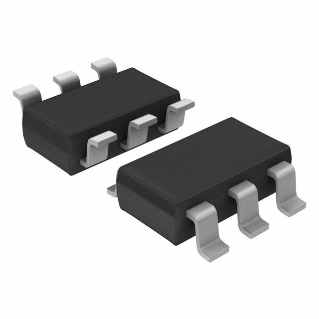
NCS2552
750 MHz Voltage
Feedback Op Amp with
Fast Enable Feature
NCS2552 is a 750 MHz voltage feedback monolithic operational
amplifier featuring high slew rate and low differential gain and phase
error. The voltage feedback architecture allows for a superior
bandwidth and low power consumption. This device features an
enable pin.
http://onsemi.com
MARKING
DIAGRAM
Features
−3.0 dB Small Signal BW (AV = +2.0, VO = 0.5 Vp−p) 750 MHz Typ
Slew Rate 1700 V/ms
Fast Enable Time 5.0 ns
Supply Current 13 mA
Input Referred Voltage Noise 5.0 nV/ ǸHz
THD −64 dBc (f = 5.0 MHz, VO = 2.0 Vp−p)
Output Current 100 mA
Pin Compatible with EL5157, AD8057
This is a Pb−Free Device
SOT23−6
(TSOP−6)
SN SUFFIX
CASE 318G
6
1
YF2, N2552
A
Y
W
G
Applications
3
NORMALIZED GAIN (dB)
6
YF2AYW
G
1
= NCS2552
= Assembly Location
= Year
= Work Week
= Pb−Free Package
SOT23−6 PINOUT
• Line Drivers
• Radar/Communication Receivers
OUT
1
VEE
2
+IN
3
6 VCC
+
•
•
•
•
•
•
•
•
•
−
5 EN
4 −IN
0
(Top View)
VOUT = 2.0 VPP
−3
VOUT = 1.0 VPP
−6
ORDERING INFORMATION
See detailed ordering and shipping information in the package
dimensions section on page 12 of this data sheet.
VOUT = 0.5 VPP
−9
−12
−15
1k
Gain = +2
VS = ±5V
RF = 150W
RL = 150W
10k
100k
1M
10M 100M
FREQUENCY (Hz)
1G
10G
Figure 1. Frequency Response:
Gain (dB) vs. Frequency Av = +2.0
© Semiconductor Components Industries, LLC, 2006
May, 2006 − Rev. 1
1
Publication Order Number:
NCS2552/D
�NCS2552
PIN FUNCTION DESCRIPTION
Pin
(SOT23/SC70)
Symbol
Function
1
OUT
Output
Equivalent Circuit
VCC
ESD
OUT
VEE
2
VEE
Negative Power Supply
3
+IN
Non−inverted Input
VCC
ESD
ESD
−IN
+IN
VEE
4
−IN
Inverted Input
6
VCC
Positive Power Supply
5
EN
Enable
See Above
VCC
EN
ESD
VEE
ENABLE PIN TRUTH TABLE
Enable
High
Low*
Disabled
Enabled
*Default open state
VCC
−IN
+IN
OUT
CC
VEE
Figure 2. Simplified Device Schematic
http://onsemi.com
2
�NCS2552
ATTRIBUTES
Characteristics
Value
ESD
Human Body Model
Machine Model
Charged Device Model
2.0 kV
200 V
1.0 kV
Moisture Sensitivity (Note 1)
Level 1
Flammability Rating
Oxygen Index: 28 to 34
UL 94 V−0 @ 0.125 in
1. For additional information, see Application Note AND8003/D.
MAXIMUM RATINGS
Parameter
Symbol
Rating
Unit
Power Supply Voltage
VS
11
Vdc
Input Voltage Range
VI
vVS
Vdc
Input Differential Voltage Range
VID
vVS
Vdc
Output Current
IO
100
mA
Maximum Junction Temperature (Note 2)
TJ
150
°C
Operating Ambient Temperature
TA
−40 to +85
°C
Storage Temperature Range
Tstg
−60 to +150
°C
Power Dissipation
PD
(See Graph)
mW
RqJA
158
°C/W
Thermal Resistance, Junction−to−Air
Stresses exceeding Maximum Ratings may damage the device. Maximum Ratings are stress ratings only. Functional operation above the
Recommended Operating Conditions is not implied. Extended exposure to stresses above the Recommended Operating Conditions may affect
device reliability.
2. Power dissipation must be considered to ensure maximum junction temperature (TJ) is not exceeded.
MAXIMUM POWER DISSIPATION (mW)
MAXIMUM POWER DISSIPATION
The maximum power that can be safely dissipated is
limited by the associated rise in junction temperature. For
the plastic packages, the maximum safe junction
temperature is 150°C. If the maximum is exceeded
momentarily, proper circuit operation will be restored as
soon as the die temperature is reduced. Leaving the device
in the “overheated’’ condition for an extended period can
result in device damage.
1400
1200
1000
800
600
400
200
0
−50
−25
0
25
50
75 100
AMBIENT TEMPERATURE (°C)
125
Figure 3. Power Dissipation vs. Temperature
http://onsemi.com
3
15
�NCS2552
AC ELECTRICAL CHARACTERISTICS (VCC = +5.0 V, VEE = −5.0 V, TA = −40°C to +85°C, RL = 150 W to GND, RF = 150 W,
AV = +2.0, Enable is left open, unless otherwise specified).
Symbol
Characteristic
Conditions
Min
Typ
Max
Unit
FREQUENCY DOMAIN PERFORMANCE
BW
GF0.1dB
Bandwidth
3.0 dB Small Signal
3.0 dB Large Signal
0.1 dB Gain Flatness
Bandwidth
MHz
AV = +2.0, VO = 0.5 Vp−p
AV = +2.0, VO = 2.0 Vp−p
750
350
AV = +2.0
40
MHz
dG
Differential Gain
AV = +2.0, RL = 150 W, f = 3.58 MHz
0.07
%
dP
Differential Phase
AV = +2.0, RL = 150 W, f = 3.58 MHz
0.01
°
Slew Rate
AV = +2.0, Vstep = 2.0 V
1700
V/ms
Settling Time
0.1%
AV = +2.0, Vstep = 2.0 V
10
(10%−90%) AV = +2.0, Vstep = 2.0 V
TIME DOMAIN RESPONSE
SR
ts
ns
tr tf
Rise and Fall Time
2.0
ns
tON
Turn−on Time
5.0
ns
tOFF
Turn−off Time
15
ns
HARMONIC/NOISE PERFORMANCE
THD
Total Harmonic Distortion
f = 5.0 MHz, VO = 2.0 Vp−p
−64
dB
HD2
2nd Harmonic Distortion
f = 5.0 MHz, VO = 2.0 Vp−p
−65
dBc
HD3
3rd Harmonic Distortion
f = 5.0 MHz, VO = 2.0 Vp−p
−75
dBc
IP3
Third−Order Intercept
f = 10 MHz, VO = 1.0 Vp−p
40
dBm
Spurious−Free Dynamic
Range
f = 5.0 MHz, VO = 2.0 Vp−p
55
dBc
SFDR
eN
Input Referred Voltage Noise
f = 1.0 MHz
5.0
nVń ǸHz
iN
Input Referred Current Noise
f = 1.0 MHz
4.0
pAń ǸHz
http://onsemi.com
4
�NCS2552
DC ELECTRICAL CHARACTERISTICS (VCC = +5.0 V, VEE = −5.0 V, TA = −40°C to +85°C, RL = 150 W to GND, RF = 150 W,
AV = +2.0, Enable is left open, unless otherwise specified).Closed Loop
Open Loop
Symbol
Characteristic
Conditions
Min
Typ
Max
Unit
−10
0
+10
mV
DC PERFORMANCE
VIO
DVIO/DT
IIB
DIIB/DT
Input Offset Voltage
Input Offset Voltage
Temperature Coefficient
6.0
Input Bias Current
VO = 0 V
"3.2
Input Bias Current
Temperature Coefficient
VO = 0 V
"40
VIH
Input High Voltage (Enable)
(Note 3)
VIL
Input Low Voltage (Enable)
(Note 3)
mV/°C
"20
mA
nA/°C
3.0
V
1.0
V
INPUT CHARACTERISTICS
VCM
CMRR
Input Common Mode Voltage
Range (Note 3)
Common Mode Rejection
Ratio
(See Graph)
"3.0
"3.2
V
40
50
dB
RIN
Input Resistance
4.5
MW
CIN
Differential Input
Capacitance
1.0
pF
0.1
13
W
OUTPUT CHARACTERISTICS
ROUT
Output Resistance
Closed Loop
Open Loop
VO
Output Voltage Range
"3.0
"4.0
V
IO
Output Current
"50
"100
mA
10
V
POWER SUPPLY
VS
Operating Voltage Supply
IS,ON
Power Supply Current −
Enabled
IS,OFF
Power Supply Current −
Disabled
PSRR
Power Supply Rejection
Ratio
5.0
(See Graph)
3. Guaranteed by design and/or characterization.
http://onsemi.com
5
40
13
17
mA
0.5
0.8
mA
56
dB
�NCS2552
AC ELECTRICAL CHARACTERISTICS (VCC = +2.5 V, VEE = −2.5 V, TA = −40°C to +85°C, RL = 150 W to GND, RF = 150 W,
AV = +2.0, Enable is left open, unless otherwise specified).
Symbol
Characteristic
Conditions
Min
Typ
Max
Unit
FREQUENCY DOMAIN PERFORMANCE
BW
GF0.1dB
Bandwidth
3.0 dB Small Signal
3.0 dB Large Signal
0.1 dB Gain Flatness
Bandwidth
MHz
AV = +2.0, VO = 0.5 Vp−p
AV = +2.0, VO = 1.0 Vp−p
550
200
AV = +2.0
35
MHz
dG
Differential Gain
AV = +2.0, RL = 150 W, f = 3.58 MHz
0.07
%
dP
Differential Phase
AV = +2.0, RL = 150 W, f = 3.58 MHz
0.02
°
Slew Rate
AV = +2.0, Vstep = 1.0 V
900
V/ms
Settling Time
0.1%
AV = +2.0, Vstep = 1.0 V
10
(10%−90%) AV = +2.0, Vstep = 1.0 V
TIME DOMAIN RESPONSE
SR
ts
ns
tr tf
Rise and Fall Time
1.7
ns
tON
Turn−on Time
5.0
ns
tOFF
Turn−off Time
15
ns
HARMONIC/NOISE PERFORMANCE
THD
Total Harmonic Distortion
f = 5.0 MHz, VO = 1.0 Vp−p
−60
dB
HD2
2nd Harmonic Distortion
f = 5.0 MHz, VO = 1.0 Vp−p
−65
dBc
HD3
3rd Harmonic Distortion
f = 5.0 MHz, VO = 1.0 Vp−p
−63
dBc
IP3
Third−Order Intercept
f = 10 MHz, VO = 0.5 Vp−p
35
dBm
Spurious−Free Dynamic
Range
f = 5.0 MHz, VO = 1.0 Vp−p
63
dBc
SFDR
eN
Input Referred Voltage Noise
f = 1.0 MHz
5.0
nVń ǸHz
iN
Input Referred Current Noise
f = 1.0 MHz
4.0
pAń ǸHz
http://onsemi.com
6
�NCS2552
DC ELECTRICAL CHARACTERISTICS (VCC = +2.5 V, VEE = −2.5 V, TA = −40°C to +85°C, RL = 150 W to GND, RF = 150 W,
AV = +2.0, Enable is left open, unless otherwise specified).
Symbol
Characteristic
Conditions
Min
Typ
Max
Unit
−10
0
+10
mV
DC PERFORMANCE
VIO
DVIO/DT
IIB
DIIB/DT
Input Offset Voltage
Input Offset Voltage
Temperature Coefficient
6.0
Input Bias Current
VO = 0 V
"3.2
Input Bias Current
Temperature Coefficient
VO = 0 V
"40
VIH
Input High Voltage (Enable)
(Note 3)
VIL
Input Low Voltage (Enable)
(Note 3)
mV/°C
"20
mA
nA/°C
1.5
V
0.5
V
INPUT CHARACTERISTICS
VCM
CMRR
Input Common Mode Voltage
Range (Note 3)
Common Mode Rejection
Ratio
(See Graph)
"1.1
"1.6
V
40
50
dB
RIN
Input Resistance
4.5
MW
CIN
Differential Input
Capacitance
1.0
pF
0.1
13
W
OUTPUT CHARACTERISTICS
ROUT
Output Resistance
Closed Loop
Open Loop
VO
Output Voltage Range
"1.1
"1.6
V
IO
Output Current
"50
"100
mA
5.0
V
POWER SUPPLY
VS
Operating Voltage Supply
IS,ON
Power Supply Current −
Enabled
IS,OFF
Power Supply Current −
Disabled
PSRR
Power Supply Rejection
Ratio
5.0
(See Graph)
40
4. Guaranteed by design and/or characterization.
VIN
+
−
VOUT
RL
RF
RF
Figure 4. Typical Test Setup
(AV = +2.0, RF = 1.0 kW, RL = 100 W)
http://onsemi.com
7
11.5
17
mA
0.5
0.8
mA
56
dB
�NCS2552
3
12
VOUT = 0.5 VPP
9
NORMALIZED GAIN (dB)
NORMALIZED GAIN (dB)
0
VOUT = 2.0 VPP
−3
VOUT = 1.0 VPP
−6
VOUT = 0.5 VPP
−9
Gain = +2
VS = ±5V
RF = 150W
RL = 150W
−12
−15
1k
10k
100k
6
3
0
−3
−6
VOUT = 1.0 VPP
−9
−12
−15
1M
10M 100M
FREQUENCY (Hz)
1G
−18
10k
10G
Figure 5. Frequency Response:
Gain (dB) vs. Frequency
Av = +2.0
Gain = +2
VOUT = 1.0 VPP
−6
Gain = +2
VOUT = 2.0 VPP
−9
−12
VS = ±5V
RF = 150W
RL = 150W
−15
100k
6
10G
1G
10G
Gain = +1
3
0
−3
−6
−9
−12
−15
1M
1G
9
0
−3
1M
10M
100M
FREQUENCY (Hz)
12
Gain = +1
VOUT = 1.0 VPP
3
100k
VOUT = 0.7 VPP
Figure 6. Frequency Response:
Gain (dB) vs. Frequency
Av = +1.0
NORMALIZED GAIN (dB)
NORMALIZED GAIN (dB)
6
Gain = +1
VS = ±5V
RF = 150W
RL = 150W
10M
100M
FREQUENCY (Hz)
−18
10k
1G
Figure 7. Large Signal Frequency Response
Gain (dB) vs. Frequency
VOUT = 0.5 VPP
VS = ±5V
RF = 150W
RL = 150W
100k
Gain = +2
1M
10M
100M
FREQUENCY (Hz)
Figure 8. Small Signal Frequency Response
Gain (dB) vs. Frequency
VS = ±5V
VS = ±5V
Figure 9. Small Signal Step Response
Vertical: 20 mV/div
Horizontal: 3 ns/div
Figure 10. Large Signal Step Response
Vertical: 1 V/div
Horizontal: 3 ns/div
http://onsemi.com
8
�NCS2552
−40
−50
−55
THD
−60
HD2
−65
HD3
−70
−50
−55
HD2
−65
HD3
−75
1
10
FREQUENCY (MHz)
−80
100
0
1
0.5
50
2
2.5
VOUT (VPP)
3
3.5
4.5
4
−20
VS = ±5V
−25
40
VS = ±5V
CMRR (dB)
−30
30
20
−35
−40
−45
10
0
−50
10
100
1k
10k
−55
10k
1M
100k
FREQUENCY (Hz)
0.08
DIFFERENTIAL GAIN (%)
VS = ±5V
−20
−30
−40
−50
−60
−70
10k
10M
100M
Figure 14. CMRR vs. Frequency
0
−10
1M
FREQUENCY (Hz)
Figure 13. Input Referred Voltage Noise vs.
Frequency
PSRR (dB)
1.5
Figure 12. THD, HD2, HD3 vs. Output Voltage
Figure 11. THD, HD2, HD3 vs. Frequency
VOLTAGE NOISE (nV/√Hz)
THD
−60
−70
−75
−80
Gain = +2
Freq = 5 MHz
VS = ±5V
RF = 150W
RL = 150W
−45
DISTORTION (dB)
−45
DISTORTION (dB)
−40
Gain = +2
VOUT = 2 VPP
VS = ±5V
RF = 150W
RL = 150W
20MHz
Gain = +2
0.06 V = ±5V
S
RF = 150W
0.04
RL = 150W
10MHz
0.02
3.58MHz
0
−0.02
4.43MHz
−0.04
−0.06
100k
1M
10M
−0.08
−0.8
100M
FREQUENCY (Hz)
−0.6
−0.4
−0.2
0
0.2
0.4
OFFSET VOLTAGE (V)
Figure 16. Differential Gain
Figure 15. PSRR vs. Frequency
http://onsemi.com
9
0.6
0.8
�NCS2552
0.03
14
20MHz
CURRENT (mA)
DIFFERENTIAL PHASE (°)
12
10MHz
0.01
3.58MHz
0
85°C
25°C
13
0.02
4.43MHz
−0.01
Gain = +2
VS = ±5V
−0.02 RF = 150W
RL = 150W
−0.03
−0.8 −0.6 −0.4
−40°C
11
10
9
8
7
0.2
0.4
−0.2
0
OFFSET VOLTAGE (V)
0.6
6
0.8
4
8
9
10
11
8
25°C
0.4
−40°C
0.35
0.3
OUTPUT VOLTAGE (VPP)
85°C
0.45
VOLTAGE (V)
7
Figure 18. Supply Current vs. Power Supply
(Enabled)
0.5
0.25
7
25°C
85°C
6
5
−40°C
4
3
2
4
5
6
7
8
CURRENT (mA)
9
10
11
5
4
Figure 19. Supply Current (Disabled)
6
7
8
9
POWER SUPPLY VOLTAGE (V)
10
11
Figure 20. Output Voltage Swing vs. Supply
Voltage
12
100
VS = ±5V
NORMALIZED GAIN (dB)
OUTPUT RESISTANCE (W)
6
POWER SUPPLY VOLTAGE (V)
Figure 17. Differential Phase
0.2
5
10
1
0.1
10pF
9
6
3
0
−3
−6
−9
0.01
10k
100k
1M
10M
100M
1G
−12
10k
10G
100pF
Gain = +2
VOUT = 0.5 VPP
VS = ±5V
RF = 150W
RL = 150W
100k
47pF
1M
10M
100M
1G
10G
FREQUENCY (Hz)
FREQUENCY (Hz)
Figure 21. Closed Loop Output Resistance vs.
Frequency
Figure 22. Frequency Response vs. Capacitive
Load
http://onsemi.com
10
�NCS2552
Output waveform: Squarewave, 32 MHz, 600 mVPP
EN
EN
VS = ±5V
OUT
OUT
VS = ±5V
Output waveform: Squarewave, 32 MHz, 600 mVPP
Figure 23. Turn ON Time Delay
Vertical: 500 mV/div (Enable), 200 mV/div (Output)
Horizontal: 5 ns/div
Figure 24. Turn OFF Time Delay
Vertical: 500 mV/div (Enable), 200 mV/div (Output)
Horizontal: 5 ns/div
http://onsemi.com
11
�NCS2552
Printed Circuit Board Layout Techniques
to input overdrive voltages above the supplies. The ESD
diodes can support high input currents with current limiting
series resistors. Keep these resistor values as low as possible
since high values degrade both noise performance and
frequency response. Under closed−loop operation, the ESD
diodes have no effect on circuit performance. However,
under certain conditions the ESD diodes will be evident. If
the device is driven into a slewing condition, the ESD diodes
will clamp large differential voltages until the feedback loop
restores closed−loop operation. Also, if the device is
powered down and a large input signal is applied, the ESD
diodes will conduct.
NOTE: Human Body Model for +IN and –IN pins are
rated at 0.8kV while all other pins are rated at
2.0kV.
Proper high speed PCB design rules should be used for all
wideband amplifiers as the PCB parasitics can affect the
overall performance. Most important are stray capacitances
at the output and inverting input nodes as it can effect
peaking and bandwidth. A space (3/16″ is plenty) should be
left around the signal lines to minimize coupling. Also,
signal lines connecting the feedback and gain resistors
should be short enough so that their associated inductance
does not cause high frequency gain errors. Line lengths less
than 1/4″ are recommended.
Video Performance
This device designed to provide good performance with
NTSC, PAL, and HDTV video signals. Best performance is
obtained with back terminated loads as performance is
degraded as the load is increased. The back termination
reduces reflections from the transmission line and
effectively masks transmission line and other parasitic
capacitances from the amplifier output stage.
VCC
Internal
Circuitry
External
Pin
ESD Protection
All device pins have limited ESD protection using internal
diodes to power supplies as specified in the attributes table
(see Figure 25). These diodes provide moderate protection
VEE
Figure 25. Internal ESD Protection
ORDERING INFORMATION
Device
NCS2552SNT1G
Package
Shipping †
SOT23−6 (TSOP−6)
(Pb−Free)
3000 Tape & Reel
†For information on tape and reel specifications, including part orientation and tape sizes, please refer to our Tape and Reel Packaging
Specifications Brochure, BRD8011/D.
http://onsemi.com
12
�MECHANICAL CASE OUTLINE
PACKAGE DIMENSIONS
TSOP−6
CASE 318G−02
ISSUE V
1
SCALE 2:1
D
H
ÉÉ
ÉÉ
6
E1
1
NOTE 5
5
2
L2
4
GAUGE
PLANE
E
3
L
b
SEATING
PLANE
C
DETAIL Z
e
DIM
A
A1
b
c
D
E
E1
e
L
L2
M
c
A
0.05
M
DATE 12 JUN 2012
NOTES:
1. DIMENSIONING AND TOLERANCING PER ASME Y14.5M, 1994.
2. CONTROLLING DIMENSION: MILLIMETERS.
3. MAXIMUM LEAD THICKNESS INCLUDES LEAD FINISH. MINIMUM
LEAD THICKNESS IS THE MINIMUM THICKNESS OF BASE MATERIAL.
4. DIMENSIONS D AND E1 DO NOT INCLUDE MOLD FLASH,
PROTRUSIONS, OR GATE BURRS. MOLD FLASH, PROTRUSIONS, OR
GATE BURRS SHALL NOT EXCEED 0.15 PER SIDE. DIMENSIONS D
AND E1 ARE DETERMINED AT DATUM H.
5. PIN ONE INDICATOR MUST BE LOCATED IN THE INDICATED ZONE.
A1
DETAIL Z
MIN
0.90
0.01
0.25
0.10
2.90
2.50
1.30
0.85
0.20
0°
MILLIMETERS
NOM
MAX
1.00
1.10
0.06
0.10
0.38
0.50
0.18
0.26
3.00
3.10
2.75
3.00
1.50
1.70
0.95
1.05
0.40
0.60
0.25 BSC
10°
−
STYLE 1:
PIN 1. DRAIN
2. DRAIN
3. GATE
4. SOURCE
5. DRAIN
6. DRAIN
STYLE 2:
PIN 1. EMITTER 2
2. BASE 1
3. COLLECTOR 1
4. EMITTER 1
5. BASE 2
6. COLLECTOR 2
STYLE 3:
PIN 1. ENABLE
2. N/C
3. R BOOST
4. Vz
5. V in
6. V out
STYLE 4:
PIN 1. N/C
2. V in
3. NOT USED
4. GROUND
5. ENABLE
6. LOAD
STYLE 5:
PIN 1. EMITTER 2
2. BASE 2
3. COLLECTOR 1
4. EMITTER 1
5. BASE 1
6. COLLECTOR 2
STYLE 6:
PIN 1. COLLECTOR
2. COLLECTOR
3. BASE
4. EMITTER
5. COLLECTOR
6. COLLECTOR
STYLE 7:
PIN 1. COLLECTOR
2. COLLECTOR
3. BASE
4. N/C
5. COLLECTOR
6. EMITTER
STYLE 8:
PIN 1. Vbus
2. D(in)
3. D(in)+
4. D(out)+
5. D(out)
6. GND
STYLE 9:
PIN 1. LOW VOLTAGE GATE
2. DRAIN
3. SOURCE
4. DRAIN
5. DRAIN
6. HIGH VOLTAGE GATE
STYLE 10:
PIN 1. D(OUT)+
2. GND
3. D(OUT)−
4. D(IN)−
5. VBUS
6. D(IN)+
STYLE 11:
PIN 1. SOURCE 1
2. DRAIN 2
3. DRAIN 2
4. SOURCE 2
5. GATE 1
6. DRAIN 1/GATE 2
STYLE 12:
PIN 1. I/O
2. GROUND
3. I/O
4. I/O
5. VCC
6. I/O
STYLE 13:
PIN 1. GATE 1
2. SOURCE 2
3. GATE 2
4. DRAIN 2
5. SOURCE 1
6. DRAIN 1
STYLE 14:
PIN 1. ANODE
2. SOURCE
3. GATE
4. CATHODE/DRAIN
5. CATHODE/DRAIN
6. CATHODE/DRAIN
STYLE 15:
PIN 1. ANODE
2. SOURCE
3. GATE
4. DRAIN
5. N/C
6. CATHODE
STYLE 16:
PIN 1. ANODE/CATHODE
2. BASE
3. EMITTER
4. COLLECTOR
5. ANODE
6. CATHODE
STYLE 17:
PIN 1. EMITTER
2. BASE
3. ANODE/CATHODE
4. ANODE
5. CATHODE
6. COLLECTOR
GENERIC
MARKING DIAGRAM*
RECOMMENDED
SOLDERING FOOTPRINT*
6X
0.60
XXXAYWG
G
1
6X
3.20
XXX
A
Y
W
G
0.95
PITCH
DIMENSIONS: MILLIMETERS
*For additional information on our Pb−Free strategy and soldering
details, please download the ON Semiconductor Soldering and
Mounting Techniques Reference Manual, SOLDERRM/D.
DOCUMENT NUMBER:
DESCRIPTION:
98ASB14888C
TSOP−6
1
IC
0.95
XXX MG
G
= Specific Device Code
=Assembly Location
= Year
= Work Week
= Pb−Free Package
STANDARD
XXX = Specific Device Code
M
= Date Code
G
= Pb−Free Package
*This information is generic. Please refer to device data sheet
for actual part marking. Pb−Free indicator, “G” or microdot “
G”, may or may not be present.
Electronic versions are uncontrolled except when accessed directly from the Document Repository.
Printed versions are uncontrolled except when stamped “CONTROLLED COPY” in red.
PAGE 1 OF 1
ON Semiconductor and
are trademarks of Semiconductor Components Industries, LLC dba ON Semiconductor or its subsidiaries in the United States and/or other countries.
ON Semiconductor reserves the right to make changes without further notice to any products herein. ON Semiconductor makes no warranty, representation or guarantee regarding
the suitability of its products for any particular purpose, nor does ON Semiconductor assume any liability arising out of the application or use of any product or circuit, and specifically
disclaims any and all liability, including without limitation special, consequential or incidental damages. ON Semiconductor does not convey any license under its patent rights nor the
rights of others.
© Semiconductor Components Industries, LLC, 2019
www.onsemi.com
�onsemi,
, and other names, marks, and brands are registered and/or common law trademarks of Semiconductor Components Industries, LLC dba “onsemi” or its affiliates
and/or subsidiaries in the United States and/or other countries. onsemi owns the rights to a number of patents, trademarks, copyrights, trade secrets, and other intellectual property.
A listing of onsemi’s product/patent coverage may be accessed at www.onsemi.com/site/pdf/Patent−Marking.pdf. onsemi reserves the right to make changes at any time to any
products or information herein, without notice. The information herein is provided “as−is” and onsemi makes no warranty, representation or guarantee regarding the accuracy of the
information, product features, availability, functionality, or suitability of its products for any particular purpose, nor does onsemi assume any liability arising out of the application or use
of any product or circuit, and specifically disclaims any and all liability, including without limitation special, consequential or incidental damages. Buyer is responsible for its products
and applications using onsemi products, including compliance with all laws, regulations and safety requirements or standards, regardless of any support or applications information
provided by onsemi. “Typical” parameters which may be provided in onsemi data sheets and/or specifications can and do vary in different applications and actual performance may
vary over time. All operating parameters, including “Typicals” must be validated for each customer application by customer’s technical experts. onsemi does not convey any license
under any of its intellectual property rights nor the rights of others. onsemi products are not designed, intended, or authorized for use as a critical component in life support systems
or any FDA Class 3 medical devices or medical devices with a same or similar classification in a foreign jurisdiction or any devices intended for implantation in the human body. Should
Buyer purchase or use onsemi products for any such unintended or unauthorized application, Buyer shall indemnify and hold onsemi and its officers, employees, subsidiaries, affiliates,
and distributors harmless against all claims, costs, damages, and expenses, and reasonable attorney fees arising out of, directly or indirectly, any claim of personal injury or death
associated with such unintended or unauthorized use, even if such claim alleges that onsemi was negligent regarding the design or manufacture of the part. onsemi is an Equal
Opportunity/Affirmative Action Employer. This literature is subject to all applicable copyright laws and is not for resale in any manner.
PUBLICATION ORDERING INFORMATION
LITERATURE FULFILLMENT:
Email Requests to: orderlit@onsemi.com
onsemi Website: www.onsemi.com
◊
TECHNICAL SUPPORT
North American Technical Support:
Voice Mail: 1 800−282−9855 Toll Free USA/Canada
Phone: 011 421 33 790 2910
Europe, Middle East and Africa Technical Support:
Phone: 00421 33 790 2910
For additional information, please contact your local Sales Representative
�