NCS29001DGEVB
NCS29001 Evaluation Board
User's�Manual
Introduction
This document gives a detailed description of the
NCS29001 Evaluation Board (SOIC-14 package) with the
bill of materials, and board schematic. The appropriate lab
test setups are also provided.
The NCS29001 Evaluation Board has been designed for
a quick evaluation of the NCS29001 LCD backlight driver.
Among its main characteristics, this evaluation board has
been constructed to boost an input voltage of 24 V to drive
an output LED string of 76 V at 200 mA.
This document must be used with the NCS29001
datasheet available on www.onsemi.com. The datasheet
contains full technical details about the NCS29001
specifications and operation. The board is implemented in
two metal layers with FR-4 dielectric. The top and bottom
layers have thicknesses of 35 mm. The total PCB thickness
is 1.62 mm with dimensions of 95.4 mm by 63.5 mm.
This evaluation board can be used to evaluate the device
performance and it allows the user to place the NCS29001
device in a real application environment. While the intention
is to evaluate the device according to datasheet
specifications, it is important to take into account the
additional circuitry inherent to the setup which can affect
performance.
http://onsemi.com
EVAL BOARD USER’S MANUAL
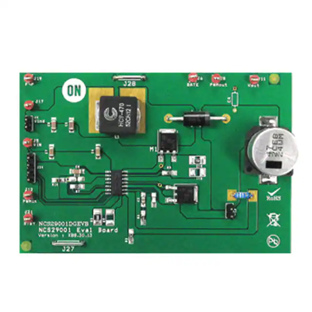
Figure 1. Evaluation Board (not to scale)
EQUIPMENT
The following table details the equipment used in the context of this application note manual.
Table 1. EQUIPMENT
Description
Regulated Power Supply
Main Features
Example of Equipment
25 V / 5 A capability or greater
Qty.
Chroma 62012P−600−8
1
Multimeter
−
Agilent 34401A
1
Oscilloscope
−
Tektronix MSO2024
1
Current probe
−
Tektronix TCP202
1
Waveform generator
−
Tektronix AFG3102
1
Get Started…
• Attach output LED string (76 V total VF)
• Set VIN = 12 V and Vinductor = 24 V
• Bring device out of standby by applying high to low
• Turning on the device from standby will trigger
•
•
soft−start power up with smooth LED current ramp up
• LED brightness can be varied by adjusting duty cycle
transition on STBY pin
Turn on device by applying PWM signal to PWMin pin
(between 100 Hz and 300 Hz with 10% to 100% duty
cycle)
© Semiconductor Components Industries, LLC, 2013
September, 2013 − Rev. 0
1
on the PWM signal
Maximum LED current is set to 200 mA for this
application
Publication Order Number:
EVBUM2213/D
�NCS29001DGEVB
SCHEMATIC
Figure 2 shows the NCS29001 in circuit as it is implemented on the evaluation board.
Figure 2. Evaluation Board Schematic
http://onsemi.com
2
�NCS29001DGEVB
BILL OF MATERIAL
Table 2. BILL OF MATERIAL
Designator
Qty
Description
Value
Tolerance
C1
1
Aluminum Electrolytic
Capacitor
47 mF
Substitution
Allowed
Lead
Free
Footprint
Manufacturer
Manufacturer Part
Number
20%
16 mm
diameter
Panasonic
EEV−EB2C470SM
Yes
Yes
C2
1
Ceramic Chip Capacitor
10 mF
10%
1206
TDK
C3216X5R1H106K160AB
Yes
Yes
C5, C7
2
Ceramic Chip Capacitor
0.1 mF
10%
1206
TDK
C3216X7R1H104K
Yes
Yes
C6, C8
2
Ceramic Chip Capacitor
1 mF
20%
1206
TDK
C3216X7R1C105M
Yes
Yes
C4
1
Aluminum Electrolytic
Capacitor
Open
−
5 mm lead
spacing
−
−
−
−
C3
1
Ceramic Chip Capacitor
3.9 nF
5%
0805
TDK
C2012C0G1H392J060AA
Yes
Yes
C11
1
Ceramic Chip Capacitor
20 pF
5%
0805
AVX
08051A200JAT2A
Yes
Yes
L1
1
High Current Inductor
47 mH
15%
14.1 mm x
13.1 mm
Cooper
Bussman
HCR−470−R
Yes
Yes
R1
1
Through Hole Resistor
499 k
1%
1 mm lead
spacing
Yageo
MFR−25FBF52−499k
Yes
Yes
R2
1
Chip Resistor
4.99 k
1%
0805
Panasonic
ERJ−6ENF4991V
Yes
Yes
R3
1
Chip Resistor
3.9 R
1%
1206
Panasonic
ERJ−8RQF3R9V
Yes
Yes
R5
1
Chip Resistor
576 R
1%
0805
Panasonic
ERJ−6ENF5760V
Yes
Yes
R6
1
Chip Resistor
715 k
1%
0805
Panasonic
ERJ−6ENF7153V
Yes
Yes
R7
1
Chip Resistor
63.4 k
1%
0805
Panasonic
ERJ−6ENF6342V
Yes
Yes
R9, R11
2
Chip Resistor
Open
−
1210
−
−
−
−
R12
1
Chip Resistor
0.075 R
1%
1206
Panasonic
ERJ−L08UF75MV
Yes
Yes
R13
1
Chip Resistor
Open
−
0805
−
−
−
−
R14
1
Chip Resistor
0
1%
0805
Panasonic
ERJ−6GEY0R00V
Yes
Yes
M1, M2
2
Power MOSFET
N−Channel
−
−
DPAK
ON
Semiconductor
NDD05N50Z
Yes
Yes
D1
1
Ultra−Fast Power
Rectifier
−
−
Axial
Lead−2
ON
Semiconductor
MUR460G
Yes
Yes
J5, J6,
J8, J11,
J12, J17,
J19, J21
8
PCB Test Terminal, Red
−
−
Hole
diameter
1.7 mm
Keystone
5005
Yes
Yes
J1, J4
2
Header 2 pin, 0.1 inch
spacing
−
−
0.100 x 2
TE
Connectivity
647676−2
Yes
Yes
J24
1
Header 4 pin, 0.1 inch
spacing
−
−
0.100 x 4
TE
Connectivity
647676−4
Yes
Yes
J27, J28
2
PCB Shorting Link
−
−
GND_Strap
Harwin
D3082−46
Yes
Yes
U1
1
NCS29001
−
−
SOIC14
ON
Semiconductor
NCS29001DR2G
No
Yes
http://onsemi.com
3
�onsemi,
, and other names, marks, and brands are registered and/or common law trademarks of Semiconductor Components Industries, LLC dba “onsemi” or its affiliates
and/or subsidiaries in the United States and/or other countries. onsemi owns the rights to a number of patents, trademarks, copyrights, trade secrets, and other intellectual property. A
listing of onsemi’s product/patent coverage may be accessed at www.onsemi.com/site/pdf/Patent−Marking.pdf. onsemi is an Equal Opportunity/Affirmative Action Employer. This
literature is subject to all applicable copyright laws and is not for resale in any manner.
The evaluation board/kit (research and development board/kit) (hereinafter the “board”) is not a finished product and is not available for sale to consumers. The board is only intended
for research, development, demonstration and evaluation purposes and will only be used in laboratory/development areas by persons with an engineering/technical training and familiar
with the risks associated with handling electrical/mechanical components, systems and subsystems. This person assumes full responsibility/liability for proper and safe handling. Any
other use, resale or redistribution for any other purpose is strictly prohibited.
THE BOARD IS PROVIDED BY ONSEMI TO YOU “AS IS” AND WITHOUT ANY REPRESENTATIONS OR WARRANTIES WHATSOEVER. WITHOUT LIMITING THE FOREGOING,
ONSEMI (AND ITS LICENSORS/SUPPLIERS) HEREBY DISCLAIMS ANY AND ALL REPRESENTATIONS AND WARRANTIES IN RELATION TO THE BOARD, ANY
MODIFICATIONS, OR THIS AGREEMENT, WHETHER EXPRESS, IMPLIED, STATUTORY OR OTHERWISE, INCLUDING WITHOUT LIMITATION ANY AND ALL
REPRESENTATIONS AND WARRANTIES OF MERCHANTABILITY, FITNESS FOR A PARTICULAR PURPOSE, TITLE, NON−INFRINGEMENT, AND THOSE ARISING FROM A
COURSE OF DEALING, TRADE USAGE, TRADE CUSTOM OR TRADE PRACTICE.
onsemi reserves the right to make changes without further notice to any board.
You are responsible for determining whether the board will be suitable for your intended use or application or will achieve your intended results. Prior to using or distributing any systems
that have been evaluated, designed or tested using the board, you agree to test and validate your design to confirm the functionality for your application. Any technical, applications or
design information or advice, quality characterization, reliability data or other services provided by onsemi shall not constitute any representation or warranty by onsemi, and no additional
obligations or liabilities shall arise from onsemi having provided such information or services.
onsemi products including the boards are not designed, intended, or authorized for use in life support systems, or any FDA Class 3 medical devices or medical devices with a similar
or equivalent classification in a foreign jurisdiction, or any devices intended for implantation in the human body. You agree to indemnify, defend and hold harmless onsemi, its directors,
officers, employees, representatives, agents, subsidiaries, affiliates, distributors, and assigns, against any and all liabilities, losses, costs, damages, judgments, and expenses, arising
out of any claim, demand, investigation, lawsuit, regulatory action or cause of action arising out of or associated with any unauthorized use, even if such claim alleges that onsemi was
negligent regarding the design or manufacture of any products and/or the board.
This evaluation board/kit does not fall within the scope of the European Union directives regarding electromagnetic compatibility, restricted substances (RoHS), recycling (WEEE), FCC,
CE or UL, and may not meet the technical requirements of these or other related directives.
FCC WARNING – This evaluation board/kit is intended for use for engineering development, demonstration, or evaluation purposes only and is not considered by onsemi to be a finished
end product fit for general consumer use. It may generate, use, or radiate radio frequency energy and has not been tested for compliance with the limits of computing devices pursuant
to part 15 of FCC rules, which are designed to provide reasonable protection against radio frequency interference. Operation of this equipment may cause interference with radio
communications, in which case the user shall be responsible, at its expense, to take whatever measures may be required to correct this interference.
onsemi does not convey any license under its patent rights nor the rights of others.
LIMITATIONS OF LIABILITY: onsemi shall not be liable for any special, consequential, incidental, indirect or punitive damages, including, but not limited to the costs of requalification,
delay, loss of profits or goodwill, arising out of or in connection with the board, even if onsemi is advised of the possibility of such damages. In no event shall onsemi’s aggregate liability
from any obligation arising out of or in connection with the board, under any theory of liability, exceed the purchase price paid for the board, if any.
The board is provided to you subject to the license and other terms per onsemi’s standard terms and conditions of sale. For more information and documentation, please visit
www.onsemi.com.
PUBLICATION ORDERING INFORMATION
LITERATURE FULFILLMENT:
Email Requests to: orderlit@onsemi.com
onsemi Website: www.onsemi.com
◊
TECHNICAL SUPPORT
North American Technical Support:
Voice Mail: 1 800−282−9855 Toll Free USA/Canada
Phone: 011 421 33 790 2910
www.onsemi.com
1
Europe, Middle East and Africa Technical Support:
Phone: 00421 33 790 2910
For additional information, please contact your local Sales Representative
�