NCS36000GEVB
NCS36000 PIR Sensor
Evaluation Board
User's Manual
General
The Passive InfraRed (PIR) sensor evaluation board is designed to
evaluate the NCS36000, a fully integrated mixed-signal CMOS device
designed for low-cost passive infrared controlling applications. This
device integrates two low-noise amplifiers and a LDO regulator to
drive the sensor. The output of the amplifiers goes to a window
comparator that uses internal voltage references from the regulator.
The detection logic processes the output from the window comparator
and provides the output to the ‘OUT’ pin. A blinking LED indicates
startup and depending on the status of the ‘LED_EN’ pin the LED also
lights up when a valid movement is detected.
The EVB can be powered from a micro-USB cable connected to
a host-USB interface (e.g. pc). Alternatively an external power source
ranging from 4–9 V can be connected to pins ‘GND’ and ‘+’ of the 3
pins header ‘H1’.
www.onsemi.com
EVAL BOARD USER’S MANUAL
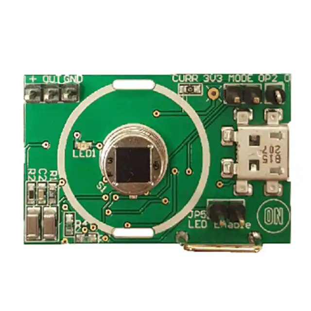
General Usage
Power the evaluation board by plugging a micro-USB cable in
connector USB1 or by connecting an external power source with
a voltage ranging 4–9 V DC between ‘GND’ and ‘+’ terminal of pin
header H1.
After power up, the LED1 starts blinking. This lasts about
30 seconds depending on the ‘TIMER’ setting. When LED1 stops
blinking, the evaluation board is ready for normal operation.
There are two potentiometers on the board. One is labeled
‘SENSITIVITY’ which controls the gain of the band-pass filter. For
more information, see the ‘Filter characteristics’ section. The other
potentiometer is labeled ‘TIMER’ and controls the system oscillator
frequency. Its setting affects the logic subsystems that determine if
a movement is detected or not. For more information see the ‘Timing
characteristics’ section.
Wave your hand above the Fresnel lens. This motion is detected
when LED1 turns on. Simultaneously the logic level on the ‘OUT’ pin
of pin header ‘H1’ is high. ‘OUT’ is the output of the digital signal
processing block. It is possible to monitor the input of the window
comparator by probing the ‘OP2_O’ test pin ‘TP2’.
The total current consumption of the application can easily be
measured by removing the 0 W jumper marked ‘CURR’ and putting an
Amp meter in series.
Jumpers JP3 (MODE) and JP5 (LED Enable) has following
function:
Figure 1. Top View of Evaluation Board
Figure 2. Bottom View of Evaluation Board
Table 1. JUMPER SETTING
Jumper
State
MODE
Open
Dual Pulse Mode
Function
MODE
Close
Single Pulse Mode
LED EN
Open
LED will Not Toggle*
LED EN
Close
LED Toggles after Motion Detected
* During start-up LED1 will blink for about 30 s. After this initialization period the
LED is disabled.
© Semiconductor Components Industries, LLC, 2015
July, 2015 − Rev. 0
1
Publication Order Number:
EVBUM2304/D
�NCS36000GEVB
H1
+
TP1
D1
U1
GND
VIN
1
OUT
5
USB1
BAV170
VBUS
C9
4,7 � F
D−
ON /
OFF
3
NR/FB
4
2
GND
3V3
CURR
MC78PC33
C10
GND_bar
C11
100 nF
R8
4,7 � F
3V3
D+
ID
GND
R7
3V3
NC
VDD
14
VREF
C6
IRA−E900
1
LDO & VREF
9
LED
12
MODE
10
XLED_EN
JP 5
JP 3
OP 1_P 5
R5
C5
3
8
WINDOW
COMPARATOR
100 nF
2
S1
6
OUT
11
DIGITAL
CONTROL
U2
680 E
LED1
OP 1_N
7
3
43 k
100 nF
VSS
OP 1_O
C2
C3
560 k
10 k
2
OP 2_N
33 � F
R1
R3
P1
10 k
OP 2_O
R7
P2 500 k
47 k
C7
20 k
100 nF
SENSITIVITY
TP2
C1
MODE
3V3
OSC
10 nF
R4
1M
LED_EN
13
1
C4
10 nF
R2
33 � F
OSC
NCS36000
4
TIMER
PC 20 150116.1
Figure 3. Schematic Diagram
Filter Characteristics
The table shows the gain and the cut-off frequencies for
different values of P1 + R4 combination, where P1is the
‘SENSITIVITY’ potentiometer.
The band-pass filter is built around 2 low noise
operational amplifiers as illustrated in Figure 3. The gain is
determined by:
G[dB] + 20 @ log
Example:
G[dB] + 20 @ log
NJƪ
1)
NJƪ
R2
R1
ƫ ƪ
@ 1)
ƫ ƪ
P1 ) R4
R3
560k
800k
1)
@ 1)
10k
10k
ƫNj
ƫNj
Table 2. GAIN SETTING
(eq. 1)
(eq. 2)
G[dB] + 73.3 dB
The lower cut-off frequency is mainly determined by
poles formed by R1 − C1 and R3 − C3. The higher cut-off
frequency is dominated by the pole formed by (P1 + R4) –
C4.
P1 + R4
Gain
f−3dB Lo
f−3dB Hi
300 kW
64.4 dB
0.72 Hz
24.3 Hz
500 kW
68.8 dB
0.71 Hz
20.4 Hz
700 kW
71.7 dB
0.71 Hz
16.7 Hz
800 kW
72.8 dB
0.70 Hz
16.0 Hz
900 kW
73.8 dB
0.70 Hz
14.8 Hz
1,1 MW
75.5 dB
0.69 Hz
13.1 Hz
1,3 MW
76.9 dB
0.69 Hz
11.7 Hz
In Figure 4 gain versus frequency is plotted for different
potentiometer settings.
www.onsemi.com
2
�NCS36000GEVB
80
Band-Pass Filter (dB)
75
70
65
60
55
50
45
40
35
100m 200m 400m
1
2
4
10
20
40
100
Frequency (Hz)
Figure 4. Gain of the Band-Pass Filter vs. Frequency; RVAR = P1 + R4
Timing Characteristics
window comparator input exceeds VH (positive threshold)
or VL (negative threshold) AND the pulse duration TSP is at
least 3 clock periods:
Potentiometer P2, marked ‘TIMER’ sets the oscillator
frequency, which is the clock of the detection system.
Changing the frequency influences the reaction time and the
sensitivity of the system.
In single pulse mode (Jumper JP3 “MODE” closed) a
signal from the sensor is detected when the amplitude at the
T SP u 3 @ T CLK
(eq. 3)
This will trigger a mono-flop and ‘OUT’ will be toggled
high for 120 clock periods.
Figure 5. Single Pulse Detection
In dual pulse mode (Jumper JP3 “MODE” removed), 2
consecutive pulses will trigger the mono-flop when the
interval TDP between these 2 consecutive pulses is less than
360 clock cycles:
T DP t 360 @ T CLK
T CLK + ǒP 2 ) R 7Ǔ @ C 7 @ 0.727
(eq. 5)
A good choice for most applications is a clock period
TCLK = 16 ms, equivalent to an oscillator frequency,
fCLK = 62.5 Hz. From equation 5 this corresponds with
P2 + R7 = 220 kW and C7 = 100 nF. By using equations 3
and 4 this results in TSP = 48 ms and TDP = 5,76 s.
(eq. 4)
The oscillator clock period depends on P2 + R7 and C7 and
can be calculated as:
www.onsemi.com
3
�NCS36000GEVB
Figure 6. Dual Pulse Detection
Interfacing Microcontroller
The easiest way to connect a MCU development PCB to
the PIR sensor evaluation board is by using pin header H1.
Power and ground connections can be shared and the logic
levels are 3,3 V compliant. By connecting “OUT” to
a general purpose I/O of the microcontroller the sensor
output can be easily monitored.
It is possible to control the evaluation board more
advanced, but this requires some additional wiring. Some
suggestions are illustrated in Figure 7 described in the next
paragraphs.
Figure 7. Schematic Diagram
The sensitivity is set by the gain of low noise amplifier 2.
See Table 2. In series of R3 a digital potentiometer can be
placed controlled by the microcontroller. P1 is removed and
R4 is set to 300 kW. See Figure 7 where a CAT5119 in the
10 k version is used needing only 2 control lines. Increasing
the gain will extend the detection range.
Motion detection is influenced by the mode of operation.
In single pulse mode the output toggles for every pulse
received under the condition the amplitude and duration are
high enough. In dual pulse mode 2 consecutive pulses need
to be detected. This avoids false detections. By connecting
the MODE input (JP3) directly to an I/O of the
microcontroller this selection can be made in software.
www.onsemi.com
4
�NCS36000GEVB
Test-point TP2 is the output of the second low noise
amplifier. It is possible to bypass the integrated Detection
Logic of NCS36000 by connecting TP2 to an ADC of an
external microcontroller. This allows the user to build
a customized detection algorithm in software.
www.onsemi.com
5
�onsemi,
, and other names, marks, and brands are registered and/or common law trademarks of Semiconductor Components Industries, LLC dba “onsemi” or its affiliates
and/or subsidiaries in the United States and/or other countries. onsemi owns the rights to a number of patents, trademarks, copyrights, trade secrets, and other intellectual property. A
listing of onsemi’s product/patent coverage may be accessed at www.onsemi.com/site/pdf/Patent−Marking.pdf. onsemi is an Equal Opportunity/Affirmative Action Employer. This
literature is subject to all applicable copyright laws and is not for resale in any manner.
The evaluation board/kit (research and development board/kit) (hereinafter the “board”) is not a finished product and is not available for sale to consumers. The board is only intended
for research, development, demonstration and evaluation purposes and will only be used in laboratory/development areas by persons with an engineering/technical training and familiar
with the risks associated with handling electrical/mechanical components, systems and subsystems. This person assumes full responsibility/liability for proper and safe handling. Any
other use, resale or redistribution for any other purpose is strictly prohibited.
THE BOARD IS PROVIDED BY ONSEMI TO YOU “AS IS” AND WITHOUT ANY REPRESENTATIONS OR WARRANTIES WHATSOEVER. WITHOUT LIMITING THE FOREGOING,
ONSEMI (AND ITS LICENSORS/SUPPLIERS) HEREBY DISCLAIMS ANY AND ALL REPRESENTATIONS AND WARRANTIES IN RELATION TO THE BOARD, ANY
MODIFICATIONS, OR THIS AGREEMENT, WHETHER EXPRESS, IMPLIED, STATUTORY OR OTHERWISE, INCLUDING WITHOUT LIMITATION ANY AND ALL
REPRESENTATIONS AND WARRANTIES OF MERCHANTABILITY, FITNESS FOR A PARTICULAR PURPOSE, TITLE, NON−INFRINGEMENT, AND THOSE ARISING FROM A
COURSE OF DEALING, TRADE USAGE, TRADE CUSTOM OR TRADE PRACTICE.
onsemi reserves the right to make changes without further notice to any board.
You are responsible for determining whether the board will be suitable for your intended use or application or will achieve your intended results. Prior to using or distributing any systems
that have been evaluated, designed or tested using the board, you agree to test and validate your design to confirm the functionality for your application. Any technical, applications or
design information or advice, quality characterization, reliability data or other services provided by onsemi shall not constitute any representation or warranty by onsemi, and no additional
obligations or liabilities shall arise from onsemi having provided such information or services.
onsemi products including the boards are not designed, intended, or authorized for use in life support systems, or any FDA Class 3 medical devices or medical devices with a similar
or equivalent classification in a foreign jurisdiction, or any devices intended for implantation in the human body. You agree to indemnify, defend and hold harmless onsemi, its directors,
officers, employees, representatives, agents, subsidiaries, affiliates, distributors, and assigns, against any and all liabilities, losses, costs, damages, judgments, and expenses, arising
out of any claim, demand, investigation, lawsuit, regulatory action or cause of action arising out of or associated with any unauthorized use, even if such claim alleges that onsemi was
negligent regarding the design or manufacture of any products and/or the board.
This evaluation board/kit does not fall within the scope of the European Union directives regarding electromagnetic compatibility, restricted substances (RoHS), recycling (WEEE), FCC,
CE or UL, and may not meet the technical requirements of these or other related directives.
FCC WARNING – This evaluation board/kit is intended for use for engineering development, demonstration, or evaluation purposes only and is not considered by onsemi to be a finished
end product fit for general consumer use. It may generate, use, or radiate radio frequency energy and has not been tested for compliance with the limits of computing devices pursuant
to part 15 of FCC rules, which are designed to provide reasonable protection against radio frequency interference. Operation of this equipment may cause interference with radio
communications, in which case the user shall be responsible, at its expense, to take whatever measures may be required to correct this interference.
onsemi does not convey any license under its patent rights nor the rights of others.
LIMITATIONS OF LIABILITY: onsemi shall not be liable for any special, consequential, incidental, indirect or punitive damages, including, but not limited to the costs of requalification,
delay, loss of profits or goodwill, arising out of or in connection with the board, even if onsemi is advised of the possibility of such damages. In no event shall onsemi’s aggregate liability
from any obligation arising out of or in connection with the board, under any theory of liability, exceed the purchase price paid for the board, if any.
The board is provided to you subject to the license and other terms per onsemi’s standard terms and conditions of sale. For more information and documentation, please visit
www.onsemi.com.
PUBLICATION ORDERING INFORMATION
LITERATURE FULFILLMENT:
Email Requests to: orderlit@onsemi.com
onsemi Website: www.onsemi.com
◊
TECHNICAL SUPPORT
North American Technical Support:
Voice Mail: 1 800−282−9855 Toll Free USA/Canada
Phone: 011 421 33 790 2910
www.onsemi.com
1
Europe, Middle East and Africa Technical Support:
Phone: 00421 33 790 2910
For additional information, please contact your local Sales Representative
�


 工商网监
湘ICP备2023018690号
工商网监
湘ICP备2023018690号
