NCS5651MNSGEVB
NCS5651MNSG
Evaluation Board
User's Manual
Introduction
www.onsemi.com
The NCS5651MNSGEVB is an evaluation board for the
NCS5651 operational amplifier.
The NCS5651 is a high efficiency, class B, low distortion
power line driver. It incorporates two operational amplifiers
(opamps). The output opamp is designed to drive up to 2 A
peak. At an output current of 1.5 A, the output voltage is
guaranteed to swing within 1 V or less of either rail, giving
the user improved SNR. In addition to the output amplifier,
a small-signal opamp is provided which can be configured
as a unity gain follower buffer or can provide a stage of
a 4-pole low pass filter.
Although the NCS5651 is designed for power line
communication (PLC) applications, it is equally suitable to
drive actuators or motors, or for any application where
a robust power amplifier is required.
For more information refer to [1, 2, 3].
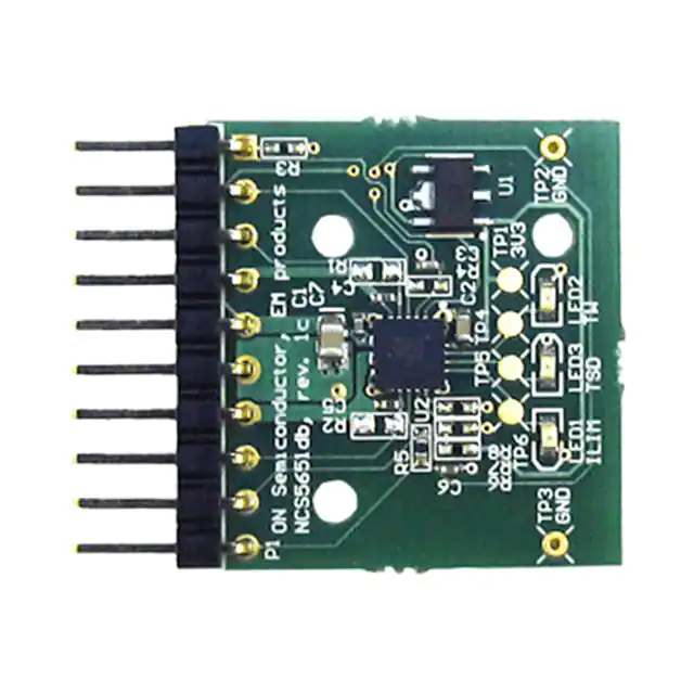
EVAL BOARD USER’S MANUAL
Description
The evaluation boards are small (26 × 23.5 mm2) printed
circuit boards (Figure 1) carrying the NCS5651 line driver.
The schematic is appended at the end of this document.
An NCP4640H033 linear regulator is provided to derive
the 3.3 V Vuc voltage. The latter determines the output
voltage of the warning output pins of the line driver. These
three pins (viz. the thermal warning flag, the thermal
shutdown flag, and the current limitation flag) are connected
to LEDs.
10. VCOM
LEDs:
Current
limitation
Thermal
shutdown
Thermal
warning
9.
Non-Inverting Input B
8.
Inverting Input B
7.
Output B
6.
Ground
5.
12 V Supply
4.
Output A
3.
Inverting Input A
2.
Non-Inverting Input A
1.
Disable
Figure 1. NCS5651MNSGEVB Outline
To ensure stability, 10 pF ceramic capacitors are fitted on
the board between the inverting input and the output of each
opamp. This must be taken into account if an external
capacitance is added, as is the case with a multi-feedback
(MFB) topology.
For convenience, a 3 kW resistor is also fitted between the
non-inverting input and Vcom. If this biasing is not required,
for instance to realize a Sallen and Key filter topology,
the resistor should be removed.
A 2.54 mm-pitch header with ten pins brings the most
important signals outside.
Besides the ground and 12 V supply pin, these include the
line driver disable and 6 V Vcom bias voltage generated by
the line driver. Both signals can be left open if unused.
All pins of the two operational amplifiers are available on
the header. As a result, any opamp topology can be realized
by fitting the appropriate external feedback and biasing
network.
© Semiconductor Components Industries, LLC, 2015
May, 2015 − Rev. 1
1
Publication Order Number:
EVBUM2288/D
�NCS5651MNSGEVB
*: on NCS5651MNSGEVB
15 kW
3 kW
56 pF
3.3 kW
*
*
10 pF
910 W
820 W
2.2 nF
10 pF
1 kW
3.3 nF
3 kW*
3 kW*
Vcom
Vcom
Figure 2. Recommended Transmission Filter for PLC with PL110 Carrier Frequencies
Figure 3. The Schematic of Figure 2 Built on Breadboard with an NCS5651MNSGEVB
Application Ideas
The size and header of the evaluation board make it
perfectly suited for breadboarding. For instance, Figure 2
shows the recommended transmission filter for PLC
S−FSK* with the PL110 carrier frequencies (105 and
115 kHz). This schematic is easily realized on breadboard
(Figure 3).
Some applications require a lower copper-to-ambient
thermal resistance (RCuA ) to improve line driver cooling.
The board design makes it possible to fit a heat sink on the
bottom side: solder mask openings and mounting holes are
foreseen.
The heat sink can be mounted with thermally conducting
adhesive tape (Figure 4). For more information on cooling,
refer to [1, 4].
Fischer Elektronik ICK SMD B 19 SA is recommended.
It may be obtained through Farnell (ref. 4302266) or Newark
(ref. 34M6437).
Figure 4. Adding a Heat Sink to Improve Cooling
*Spread-frequency shift keying (S−FSK) is a modulation scheme
widely used in power line communication (PLC). It combines
simplicity (and thus allows a low cost implementation) with good
resilience.
www.onsemi.com
2
�12V
12V
C7
100n/25
21
10
11
6
7
C3
100n/16
C6
100n/16
R6
1k3
Vw
3V3d
VEE
VEE
VEE
Vcc
Vcc
Thermal warming set at 80°C
OutB
B−
B+
Vcom
1
2
3
4
5
6
7
8
9
10
En
R7 R8
3k 10k
18
17
16
20
19
LED1
LED3
TWflag
TSDflag
ILIMflag
3V3d
U2A
NCS5651
C1
10u/25
Current limitation set at 1 A.
TW_FLAG
TSD_FLAG
I_LIM_FLAG
GND_uC
V_uC
R3
51k
12V
5
3
U1
NCP4640H033T1G
1
VIN
VOUT
CE
GND
GND
LED2
TP4
TW TP5
TSD TP6
ILIM
TP3
GND
TP2
GND
2
4
En
A+
A−
OutA
Vcom
2
Vcom
V_Warn
1
Enable
R_Lim
www.onsemi.com
14
Figure 5. NCS5651MNSGEVB Schematic
15
3
A+
A−
R4
3k
C2
1u/10
3
4
OutA
B−
U2B
NCS5651
5
10p/C0G
R5
3k
B+
12
13
?
U2C
NCS5651
10p/C0G
C5
?
C4
R2
Vcom
R1
−A
OutA
+A
TP1
3v3
3V3d
Vcom
P1
Header 10 right angle
8
9
OutB
NCS5651MNSGEVB
�NCS5651MNSGEVB
References
[1] ON Semiconductor. Evaluation kit for power-line
communication user manual, December 2014.
[2] ON Semiconductor. Getting started with power line
communication (application note AND9165/D),
June 2014. Online at www.onsemi.com/pub_link/
Collateral/AND9165−D.PDF.
[3] ON Semiconductor. NCS5651 2 Amp PLC line
driver datasheet, December 2014.
Online at www.onsemi.com/pub_link/
Collateral/NCS5651−D.PDF.
[4] ON Semiconductor, Roger Stout. Thermal
considerations for the NCS5651
(application note AND8402/D), August 2014.
Online at www.onsemi.com/pub_link/
Collateral/AND8402−D.PDF.
www.onsemi.com
4
�onsemi,
, and other names, marks, and brands are registered and/or common law trademarks of Semiconductor Components Industries, LLC dba “onsemi” or its affiliates
and/or subsidiaries in the United States and/or other countries. onsemi owns the rights to a number of patents, trademarks, copyrights, trade secrets, and other intellectual property. A
listing of onsemi’s product/patent coverage may be accessed at www.onsemi.com/site/pdf/Patent−Marking.pdf. onsemi is an Equal Opportunity/Affirmative Action Employer. This
literature is subject to all applicable copyright laws and is not for resale in any manner.
The evaluation board/kit (research and development board/kit) (hereinafter the “board”) is not a finished product and is not available for sale to consumers. The board is only intended
for research, development, demonstration and evaluation purposes and will only be used in laboratory/development areas by persons with an engineering/technical training and familiar
with the risks associated with handling electrical/mechanical components, systems and subsystems. This person assumes full responsibility/liability for proper and safe handling. Any
other use, resale or redistribution for any other purpose is strictly prohibited.
THE BOARD IS PROVIDED BY ONSEMI TO YOU “AS IS” AND WITHOUT ANY REPRESENTATIONS OR WARRANTIES WHATSOEVER. WITHOUT LIMITING THE FOREGOING,
ONSEMI (AND ITS LICENSORS/SUPPLIERS) HEREBY DISCLAIMS ANY AND ALL REPRESENTATIONS AND WARRANTIES IN RELATION TO THE BOARD, ANY
MODIFICATIONS, OR THIS AGREEMENT, WHETHER EXPRESS, IMPLIED, STATUTORY OR OTHERWISE, INCLUDING WITHOUT LIMITATION ANY AND ALL
REPRESENTATIONS AND WARRANTIES OF MERCHANTABILITY, FITNESS FOR A PARTICULAR PURPOSE, TITLE, NON−INFRINGEMENT, AND THOSE ARISING FROM A
COURSE OF DEALING, TRADE USAGE, TRADE CUSTOM OR TRADE PRACTICE.
onsemi reserves the right to make changes without further notice to any board.
You are responsible for determining whether the board will be suitable for your intended use or application or will achieve your intended results. Prior to using or distributing any systems
that have been evaluated, designed or tested using the board, you agree to test and validate your design to confirm the functionality for your application. Any technical, applications or
design information or advice, quality characterization, reliability data or other services provided by onsemi shall not constitute any representation or warranty by onsemi, and no additional
obligations or liabilities shall arise from onsemi having provided such information or services.
onsemi products including the boards are not designed, intended, or authorized for use in life support systems, or any FDA Class 3 medical devices or medical devices with a similar
or equivalent classification in a foreign jurisdiction, or any devices intended for implantation in the human body. You agree to indemnify, defend and hold harmless onsemi, its directors,
officers, employees, representatives, agents, subsidiaries, affiliates, distributors, and assigns, against any and all liabilities, losses, costs, damages, judgments, and expenses, arising
out of any claim, demand, investigation, lawsuit, regulatory action or cause of action arising out of or associated with any unauthorized use, even if such claim alleges that onsemi was
negligent regarding the design or manufacture of any products and/or the board.
This evaluation board/kit does not fall within the scope of the European Union directives regarding electromagnetic compatibility, restricted substances (RoHS), recycling (WEEE), FCC,
CE or UL, and may not meet the technical requirements of these or other related directives.
FCC WARNING – This evaluation board/kit is intended for use for engineering development, demonstration, or evaluation purposes only and is not considered by onsemi to be a finished
end product fit for general consumer use. It may generate, use, or radiate radio frequency energy and has not been tested for compliance with the limits of computing devices pursuant
to part 15 of FCC rules, which are designed to provide reasonable protection against radio frequency interference. Operation of this equipment may cause interference with radio
communications, in which case the user shall be responsible, at its expense, to take whatever measures may be required to correct this interference.
onsemi does not convey any license under its patent rights nor the rights of others.
LIMITATIONS OF LIABILITY: onsemi shall not be liable for any special, consequential, incidental, indirect or punitive damages, including, but not limited to the costs of requalification,
delay, loss of profits or goodwill, arising out of or in connection with the board, even if onsemi is advised of the possibility of such damages. In no event shall onsemi’s aggregate liability
from any obligation arising out of or in connection with the board, under any theory of liability, exceed the purchase price paid for the board, if any.
The board is provided to you subject to the license and other terms per onsemi’s standard terms and conditions of sale. For more information and documentation, please visit
www.onsemi.com.
PUBLICATION ORDERING INFORMATION
LITERATURE FULFILLMENT:
Email Requests to: orderlit@onsemi.com
onsemi Website: www.onsemi.com
◊
TECHNICAL SUPPORT
North American Technical Support:
Voice Mail: 1 800−282−9855 Toll Free USA/Canada
Phone: 011 421 33 790 2910
www.onsemi.com
1
Europe, Middle East and Africa Technical Support:
Phone: 00421 33 790 2910
For additional information, please contact your local Sales Representative
�


 工商网监
湘ICP备2023018690号
工商网监
湘ICP备2023018690号
