NCV1009
2.5 Volt Reference
The NCV1009 is a precision trimmed 2.5 V ±5.0 mV shunt
regulator diode. The low dynamic impedance and wide operating
current range enhances its versatility. The tight reference tolerance is
achieved by on−chip trimming which minimizes voltage tolerance and
temperature drift.
A third terminal allows the reference voltage to be adjusted ±5.0%
to calibrate out system errors. In many applications, the NCV1009Z
can be used as a pin−to−pin replacement of the LT1009CZ and the
LM136Z−2.5 with the external trim network eliminated.
Features
• 0.2% Initial Tolerance Max.
• Guaranteed Temperature Stability
• Maximum 0.6 W Dynamic Impedance
• Wide Operating Current Range
• Directly Interchangeable with LT1009 and LM136 for Improved
Performance
• No Adjustments Needed for Minimum Temperature Coefficient
• Meets Mil Std 883C ESD Requirements
• Extended Operating Temperature Range for Use in Automotive
Applications
• NCV Prefix, for Automotive and Other Applications Requiring Site
and Change Control
• Pb−Free Packages are Available
http://onsemi.com
MARKING
DIAGRAMS
8
SOIC−8
D SUFFIX
CASE 751
8
1
1009D
ALYW
G
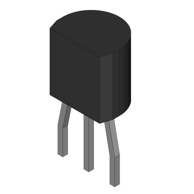
1
TO−92
Z SUFFIX
CASE 29
A
L
Y
WW, W
G
1009Z
ALYWWG
G
= Assembly Location
= Wafer Lot
= Year
= Work Week
= Pb−Free Package
(Note: Microdot may be in either location)
PIN CONNECTIONS
NC
1
8
NC
NC
NC
NC
VREF
GND
ADJ. PIN
5.0 V−35 V
Pin 1. ADJ. PIN
2. VREF
3. GND
3.6 kW
1 2 3
VREF
ORDERING INFORMATION
ADJ
10 kW∗
TRIM
Device
GND
If the external trim resistor is not used, the “ADJ. PIN” should
be left floating. The 10k trim potentiometer does not effect the
temperature coefficient of the device.
Figure 1. Application Diagram
February, 2006 − Rev. 9
Shipping
NCV1009D
SOIC−8
95 Units/Rail
NCV1009DR2
SOIC−8
2500 Tape & Reel
SOIC−8
(Pb−Free)
2500 Tape & Reel
TO−92
2000 Units/Rail
TO−92
(Pb−Free)
2000 Tape & Reel
NCV1009DR2G
*±5.0% Trim Range
© Semiconductor Components Industries, LLC, 2006
Package
NCV1009Z
NCV1009ZG
†For information on tape and reel specifications,
including part orientation and tape sizes, please
refer to our Tape and Reel Packaging Specification
Brochure, BRD8011/D.
1
Publication Order Number:
NCV1009/D
�NCV1009
VREF
P3
10 pF
15 pF
N14
TRIM
P2
P1
N16
14 kW
20 kW
20 pF
20 kW
10.15 kW
63 kW
N7
N2
N8
N12 N13
30 kW
N1
N4
N3
ADJ
N10
N9
N5
N6
1.14 kW
SUBSTRATE
GND
Figure 2. Block Diagram
http://onsemi.com
2
N11
1.14 kW
6.785 kW
D1
N15
�NCV1009
MAXIMUM RATINGS*
Rating
Value
Unit
Reverse Current
20
mA
Forward
10
mA
45
165
°C/W
°C/W
−
170
°C/W
°C/W
Operating Temperature Range
−40 to +125
°C
Storage Temperature Range
−65 to +150
°C
260 peak
240 peak
°C
°C
Package Thermal Resistance, SOIC−8:
Junction−to−Case, RqJC
Junction−to−Ambient, RqJA
Package Thermal Resistance, TO−92:
Junction−to−Case, RqJC
Junction−to−Ambient, RqJA
Lead Temperature Soldering:
Wave Solder (through hole styles only) (Note 1)
Reflow: (SMD styles only) (Notes 2, 3)
Maximum ratings are those values beyond which device damage can occur. Maximum ratings applied to the device are individual stress limit
values (not normal operating conditions) and are not valid simultaneously. If these limits are exceeded, device functional operation is not implied,
damage may occur and reliability may be affected.
*The maximum package power dissipation must be observed.
1. 10 second maximum
2. 60 second maximum above 183°C.
3. −5°C / +0°C allowable conditions.
ELECTRICAL CHARACTERISTICS (TA = 25°C unless otherwise specified.)
Characteristic
Test Conditions
Min
Typ
Max
Unit
Reverse Breakdown Voltage
IR = 1.0 mA
2.492
2.500
2.508
V
Reverse Breakdown Voltage
−40°C ≤ TA ≤ 125°C
2.480
2.500
2.508
V
Reverse Breakdown Voltage
Change with Current
400 mA ≤ IR ≤ 10 mA
(Note 4)
−
−
2.6
3.0
5.0
6.0
mV
mV
Reverse Dynamic Impedance
IR = 1.0 mA
(Note 4)
−
−
0.2
0.4
1.0
1.4
W
W
Temperature Stability
Average Temperature Coefficient
0°C ≤ TA ≤ 70°C, (Note 5)
0°C ≤ TA ≤ 70°C, (Note 5)
−
−
1.8
15
−
−
mV
ppm/°C
Long Term Stabilty
TA = 25°C ±0.1 C, IR = 1.0 mA
−
20
−
ppm/kHr
4. Denotes the specifications which apply over full operating temperature range.
5. Average temperature coefficient is defined as the total voltage change divided by the specified temperature range.
http://onsemi.com
3
�NCV1009
TYPICAL PERFORMANCE CHARACTERISTICS
5
REVERSE VOLTAGE CHANGE (mV)
REVERSE CURRENT (A)
10−1
10−2
10−3
10−4
TJ = 25°C
10−5
0.5
1.0
1.4
1.8
REVERSE VOLTAGE (V)
4
3
2
1
0
2.6
2.2
0
4
Figure 3. Reverse Current vs. Reverse Voltage
20
Figure 4. Change in Reverse Voltage vs.
Reverse Current
1.2
100
TJ = 25°C
DYNAMIC IMPEDANCE (W)
FORWARD VOLTAGE (V)
8
12
16
REVERSE CURRENT (mA)
1.0
0.8
0.6
0.4
0.2
0
0.001
0.01
0.1
1.0
10
1.0
0.1
10
10
100
FORWARD CURRENT (mA)
Figure 5. Forward Voltage vs. Forward Current
1.0 k
10 k
FREQUENCY (Hz)
100 k
Figure 6. Dynamic Impedance vs. Frequency
IR = ImA
TJ = 25°C
0
VOLTAGE SWING (V)
NOISE (nV/√HZ)
FORWARD VOLTAGE (V)
250
200
150
2.5
2.0
1.5
5.0 k
1.0
0.5
0
INPUT
OUTPUT
100
10.0
4.0
0
50
10
100
1.0 k
FREQUENCY (Hz)
10 k
100 k
Figure 7. Zener Noise Voltage vs. Frequency
0
1
TIME (ms)
Figure 8. Response Time
http://onsemi.com
4
20
�MECHANICAL CASE OUTLINE
PACKAGE DIMENSIONS
TO−92 (TO−226)
CASE 29−11
ISSUE AM
SCALE 1:1
1
12
3
STRAIGHT LEAD
BULK PACK
DATE 09 MAR 2007
2
3
BENT LEAD
TAPE & REEL
AMMO PACK
A
B
NOTES:
1. DIMENSIONING AND TOLERANCING PER ANSI
Y14.5M, 1982.
2. CONTROLLING DIMENSION: INCH.
3. CONTOUR OF PACKAGE BEYOND DIMENSION R
IS UNCONTROLLED.
4. LEAD DIMENSION IS UNCONTROLLED IN P AND
BEYOND DIMENSION K MINIMUM.
STRAIGHT LEAD
BULK PACK
R
P
L
SEATING
PLANE
K
DIM
A
B
C
D
G
H
J
K
L
N
P
R
V
D
X X
G
J
H
V
C
SECTION X−X
N
1
INCHES
MIN
MAX
0.175
0.205
0.170
0.210
0.125
0.165
0.016
0.021
0.045
0.055
0.095
0.105
0.015
0.020
0.500
--0.250
--0.080
0.105
--0.100
0.115
--0.135
---
MILLIMETERS
MIN
MAX
4.45
5.20
4.32
5.33
3.18
4.19
0.407
0.533
1.15
1.39
2.42
2.66
0.39
0.50
12.70
--6.35
--2.04
2.66
--2.54
2.93
--3.43
---
N
A
R
NOTES:
1. DIMENSIONING AND TOLERANCING PER
ASME Y14.5M, 1994.
2. CONTROLLING DIMENSION: MILLIMETERS.
3. CONTOUR OF PACKAGE BEYOND
DIMENSION R IS UNCONTROLLED.
4. LEAD DIMENSION IS UNCONTROLLED IN P
AND BEYOND DIMENSION K MINIMUM.
BENT LEAD
TAPE & REEL
AMMO PACK
B
P
T
SEATING
PLANE
G
K
DIM
A
B
C
D
G
J
K
N
P
R
V
D
X X
J
V
1
C
N
SECTION X−X
MILLIMETERS
MIN
MAX
4.45
5.20
4.32
5.33
3.18
4.19
0.40
0.54
2.40
2.80
0.39
0.50
12.70
--2.04
2.66
1.50
4.00
2.93
--3.43
---
STYLES ON PAGE 2
DOCUMENT NUMBER:
STATUS:
98ASB42022B
ON SEMICONDUCTOR STANDARD
NEW STANDARD:
© Semiconductor Components Industries, LLC, 2002
October, DESCRIPTION:
2002 − Rev. 0
TO−92 (TO−226)
http://onsemi.com
1
Electronic versions are uncontrolled except when
accessed directly from the Document Repository. Printed
versions are uncontrolled except when stamped
“CONTROLLED COPY” in red.
Case Outline Number:
PAGE 1 OFXXX
3
�TO−92 (TO−226)
CASE 29−11
ISSUE AM
DATE 09 MAR 2007
STYLE 1:
PIN 1. EMITTER
2. BASE
3. COLLECTOR
STYLE 2:
PIN 1. BASE
2. EMITTER
3. COLLECTOR
STYLE 3:
PIN 1. ANODE
2. ANODE
3. CATHODE
STYLE 4:
PIN 1. CATHODE
2. CATHODE
3. ANODE
STYLE 5:
PIN 1. DRAIN
2. SOURCE
3. GATE
STYLE 6:
PIN 1. GATE
2. SOURCE & SUBSTRATE
3. DRAIN
STYLE 7:
PIN 1. SOURCE
2. DRAIN
3. GATE
STYLE 8:
PIN 1. DRAIN
2. GATE
3. SOURCE & SUBSTRATE
STYLE 9:
PIN 1. BASE 1
2. EMITTER
3. BASE 2
STYLE 10:
PIN 1. CATHODE
2. GATE
3. ANODE
STYLE 11:
PIN 1. ANODE
2. CATHODE & ANODE
3. CATHODE
STYLE 12:
PIN 1. MAIN TERMINAL 1
2. GATE
3. MAIN TERMINAL 2
STYLE 13:
PIN 1. ANODE 1
2. GATE
3. CATHODE 2
STYLE 14:
PIN 1. EMITTER
2. COLLECTOR
3. BASE
STYLE 15:
PIN 1. ANODE 1
2. CATHODE
3. ANODE 2
STYLE 16:
PIN 1. ANODE
2. GATE
3. CATHODE
STYLE 17:
PIN 1. COLLECTOR
2. BASE
3. EMITTER
STYLE 18:
PIN 1. ANODE
2. CATHODE
3. NOT CONNECTED
STYLE 19:
PIN 1. GATE
2. ANODE
3. CATHODE
STYLE 20:
PIN 1. NOT CONNECTED
2. CATHODE
3. ANODE
STYLE 21:
PIN 1. COLLECTOR
2. EMITTER
3. BASE
STYLE 22:
PIN 1. SOURCE
2. GATE
3. DRAIN
STYLE 23:
PIN 1. GATE
2. SOURCE
3. DRAIN
STYLE 24:
PIN 1. EMITTER
2. COLLECTOR/ANODE
3. CATHODE
STYLE 25:
PIN 1. MT 1
2. GATE
3. MT 2
STYLE 26:
PIN 1. VCC
2. GROUND 2
3. OUTPUT
STYLE 27:
PIN 1. MT
2. SUBSTRATE
3. MT
STYLE 28:
PIN 1. CATHODE
2. ANODE
3. GATE
STYLE 29:
PIN 1. NOT CONNECTED
2. ANODE
3. CATHODE
STYLE 30:
PIN 1. DRAIN
2. GATE
3. SOURCE
STYLE 31:
PIN 1. GATE
2. DRAIN
3. SOURCE
STYLE 32:
PIN 1. BASE
2. COLLECTOR
3. EMITTER
STYLE 33:
PIN 1. RETURN
2. INPUT
3. OUTPUT
STYLE 34:
PIN 1. INPUT
2. GROUND
3. LOGIC
STYLE 35:
PIN 1. GATE
2. COLLECTOR
3. EMITTER
DOCUMENT NUMBER:
STATUS:
98ASB42022B
ON SEMICONDUCTOR STANDARD
NEW STANDARD:
© Semiconductor Components Industries, LLC, 2002
October, DESCRIPTION:
2002 − Rev. 0
TO−92 (TO−226)
http://onsemi.com
2
Electronic versions are uncontrolled except when
accessed directly from the Document Repository. Printed
versions are uncontrolled except when stamped
“CONTROLLED COPY” in red.
Case Outline Number:
PAGE 2 OFXXX
3
�DOCUMENT NUMBER:
98ASB42022B
PAGE 3 OF 3
ISSUE
AM
REVISION
ADDED BENT−LEAD TAPE & REEL VERSION. REQ. BY J. SUPINA.
DATE
09 MAR 2007
ON Semiconductor and
are registered trademarks of Semiconductor Components Industries, LLC (SCILLC). SCILLC reserves the right to make changes without further notice
to any products herein. SCILLC makes no warranty, representation or guarantee regarding the suitability of its products for any particular purpose, nor does SCILLC assume any liability
arising out of the application or use of any product or circuit, and specifically disclaims any and all liability, including without limitation special, consequential or incidental damages.
“Typical” parameters which may be provided in SCILLC data sheets and/or specifications can and do vary in different applications and actual performance may vary over time. All
operating parameters, including “Typicals” must be validated for each customer application by customer’s technical experts. SCILLC does not convey any license under its patent rights
nor the rights of others. SCILLC products are not designed, intended, or authorized for use as components in systems intended for surgical implant into the body, or other applications
intended to support or sustain life, or for any other application in which the failure of the SCILLC product could create a situation where personal injury or death may occur. Should
Buyer purchase or use SCILLC products for any such unintended or unauthorized application, Buyer shall indemnify and hold SCILLC and its officers, employees, subsidiaries, affiliates,
and distributors harmless against all claims, costs, damages, and expenses, and reasonable attorney fees arising out of, directly or indirectly, any claim of personal injury or death
associated with such unintended or unauthorized use, even if such claim alleges that SCILLC was negligent regarding the design or manufacture of the part. SCILLC is an Equal
Opportunity/Affirmative Action Employer. This literature is subject to all applicable copyright laws and is not for resale in any manner.
© Semiconductor Components Industries, LLC, 2007
March, 2007 − Rev. 11AM
Case Outline Number:
29
�MECHANICAL CASE OUTLINE
PACKAGE DIMENSIONS
SOIC−8 NB
CASE 751−07
ISSUE AK
8
1
SCALE 1:1
−X−
DATE 16 FEB 2011
NOTES:
1. DIMENSIONING AND TOLERANCING PER
ANSI Y14.5M, 1982.
2. CONTROLLING DIMENSION: MILLIMETER.
3. DIMENSION A AND B DO NOT INCLUDE
MOLD PROTRUSION.
4. MAXIMUM MOLD PROTRUSION 0.15 (0.006)
PER SIDE.
5. DIMENSION D DOES NOT INCLUDE DAMBAR
PROTRUSION. ALLOWABLE DAMBAR
PROTRUSION SHALL BE 0.127 (0.005) TOTAL
IN EXCESS OF THE D DIMENSION AT
MAXIMUM MATERIAL CONDITION.
6. 751−01 THRU 751−06 ARE OBSOLETE. NEW
STANDARD IS 751−07.
A
8
5
S
B
0.25 (0.010)
M
Y
M
1
4
−Y−
K
G
C
N
X 45 _
SEATING
PLANE
−Z−
0.10 (0.004)
H
M
D
0.25 (0.010)
M
Z Y
S
X
J
S
8
8
1
1
IC
4.0
0.155
XXXXX
A
L
Y
W
G
IC
(Pb−Free)
= Specific Device Code
= Assembly Location
= Wafer Lot
= Year
= Work Week
= Pb−Free Package
XXXXXX
AYWW
1
1
Discrete
XXXXXX
AYWW
G
Discrete
(Pb−Free)
XXXXXX = Specific Device Code
A
= Assembly Location
Y
= Year
WW
= Work Week
G
= Pb−Free Package
*This information is generic. Please refer to
device data sheet for actual part marking.
Pb−Free indicator, “G” or microdot “G”, may
or may not be present. Some products may
not follow the Generic Marking.
1.270
0.050
SCALE 6:1
INCHES
MIN
MAX
0.189
0.197
0.150
0.157
0.053
0.069
0.013
0.020
0.050 BSC
0.004
0.010
0.007
0.010
0.016
0.050
0 _
8 _
0.010
0.020
0.228
0.244
8
8
XXXXX
ALYWX
G
XXXXX
ALYWX
1.52
0.060
0.6
0.024
MILLIMETERS
MIN
MAX
4.80
5.00
3.80
4.00
1.35
1.75
0.33
0.51
1.27 BSC
0.10
0.25
0.19
0.25
0.40
1.27
0_
8_
0.25
0.50
5.80
6.20
GENERIC
MARKING DIAGRAM*
SOLDERING FOOTPRINT*
7.0
0.275
DIM
A
B
C
D
G
H
J
K
M
N
S
mm Ǔ
ǒinches
*For additional information on our Pb−Free strategy and soldering
details, please download the ON Semiconductor Soldering and
Mounting Techniques Reference Manual, SOLDERRM/D.
STYLES ON PAGE 2
DOCUMENT NUMBER:
DESCRIPTION:
98ASB42564B
SOIC−8 NB
Electronic versions are uncontrolled except when accessed directly from the Document Repository.
Printed versions are uncontrolled except when stamped “CONTROLLED COPY” in red.
PAGE 1 OF 2
onsemi and
are trademarks of Semiconductor Components Industries, LLC dba onsemi or its subsidiaries in the United States and/or other countries. onsemi reserves
the right to make changes without further notice to any products herein. onsemi makes no warranty, representation or guarantee regarding the suitability of its products for any particular
purpose, nor does onsemi assume any liability arising out of the application or use of any product or circuit, and specifically disclaims any and all liability, including without limitation
special, consequential or incidental damages. onsemi does not convey any license under its patent rights nor the rights of others.
© Semiconductor Components Industries, LLC, 2019
www.onsemi.com
�SOIC−8 NB
CASE 751−07
ISSUE AK
DATE 16 FEB 2011
STYLE 1:
PIN 1. EMITTER
2. COLLECTOR
3. COLLECTOR
4. EMITTER
5. EMITTER
6. BASE
7. BASE
8. EMITTER
STYLE 2:
PIN 1. COLLECTOR, DIE, #1
2. COLLECTOR, #1
3. COLLECTOR, #2
4. COLLECTOR, #2
5. BASE, #2
6. EMITTER, #2
7. BASE, #1
8. EMITTER, #1
STYLE 3:
PIN 1. DRAIN, DIE #1
2. DRAIN, #1
3. DRAIN, #2
4. DRAIN, #2
5. GATE, #2
6. SOURCE, #2
7. GATE, #1
8. SOURCE, #1
STYLE 4:
PIN 1. ANODE
2. ANODE
3. ANODE
4. ANODE
5. ANODE
6. ANODE
7. ANODE
8. COMMON CATHODE
STYLE 5:
PIN 1. DRAIN
2. DRAIN
3. DRAIN
4. DRAIN
5. GATE
6. GATE
7. SOURCE
8. SOURCE
STYLE 6:
PIN 1. SOURCE
2. DRAIN
3. DRAIN
4. SOURCE
5. SOURCE
6. GATE
7. GATE
8. SOURCE
STYLE 7:
PIN 1. INPUT
2. EXTERNAL BYPASS
3. THIRD STAGE SOURCE
4. GROUND
5. DRAIN
6. GATE 3
7. SECOND STAGE Vd
8. FIRST STAGE Vd
STYLE 8:
PIN 1. COLLECTOR, DIE #1
2. BASE, #1
3. BASE, #2
4. COLLECTOR, #2
5. COLLECTOR, #2
6. EMITTER, #2
7. EMITTER, #1
8. COLLECTOR, #1
STYLE 9:
PIN 1. EMITTER, COMMON
2. COLLECTOR, DIE #1
3. COLLECTOR, DIE #2
4. EMITTER, COMMON
5. EMITTER, COMMON
6. BASE, DIE #2
7. BASE, DIE #1
8. EMITTER, COMMON
STYLE 10:
PIN 1. GROUND
2. BIAS 1
3. OUTPUT
4. GROUND
5. GROUND
6. BIAS 2
7. INPUT
8. GROUND
STYLE 11:
PIN 1. SOURCE 1
2. GATE 1
3. SOURCE 2
4. GATE 2
5. DRAIN 2
6. DRAIN 2
7. DRAIN 1
8. DRAIN 1
STYLE 12:
PIN 1. SOURCE
2. SOURCE
3. SOURCE
4. GATE
5. DRAIN
6. DRAIN
7. DRAIN
8. DRAIN
STYLE 13:
PIN 1. N.C.
2. SOURCE
3. SOURCE
4. GATE
5. DRAIN
6. DRAIN
7. DRAIN
8. DRAIN
STYLE 14:
PIN 1. N−SOURCE
2. N−GATE
3. P−SOURCE
4. P−GATE
5. P−DRAIN
6. P−DRAIN
7. N−DRAIN
8. N−DRAIN
STYLE 15:
PIN 1. ANODE 1
2. ANODE 1
3. ANODE 1
4. ANODE 1
5. CATHODE, COMMON
6. CATHODE, COMMON
7. CATHODE, COMMON
8. CATHODE, COMMON
STYLE 16:
PIN 1. EMITTER, DIE #1
2. BASE, DIE #1
3. EMITTER, DIE #2
4. BASE, DIE #2
5. COLLECTOR, DIE #2
6. COLLECTOR, DIE #2
7. COLLECTOR, DIE #1
8. COLLECTOR, DIE #1
STYLE 17:
PIN 1. VCC
2. V2OUT
3. V1OUT
4. TXE
5. RXE
6. VEE
7. GND
8. ACC
STYLE 18:
PIN 1. ANODE
2. ANODE
3. SOURCE
4. GATE
5. DRAIN
6. DRAIN
7. CATHODE
8. CATHODE
STYLE 19:
PIN 1. SOURCE 1
2. GATE 1
3. SOURCE 2
4. GATE 2
5. DRAIN 2
6. MIRROR 2
7. DRAIN 1
8. MIRROR 1
STYLE 20:
PIN 1. SOURCE (N)
2. GATE (N)
3. SOURCE (P)
4. GATE (P)
5. DRAIN
6. DRAIN
7. DRAIN
8. DRAIN
STYLE 21:
PIN 1. CATHODE 1
2. CATHODE 2
3. CATHODE 3
4. CATHODE 4
5. CATHODE 5
6. COMMON ANODE
7. COMMON ANODE
8. CATHODE 6
STYLE 22:
PIN 1. I/O LINE 1
2. COMMON CATHODE/VCC
3. COMMON CATHODE/VCC
4. I/O LINE 3
5. COMMON ANODE/GND
6. I/O LINE 4
7. I/O LINE 5
8. COMMON ANODE/GND
STYLE 23:
PIN 1. LINE 1 IN
2. COMMON ANODE/GND
3. COMMON ANODE/GND
4. LINE 2 IN
5. LINE 2 OUT
6. COMMON ANODE/GND
7. COMMON ANODE/GND
8. LINE 1 OUT
STYLE 24:
PIN 1. BASE
2. EMITTER
3. COLLECTOR/ANODE
4. COLLECTOR/ANODE
5. CATHODE
6. CATHODE
7. COLLECTOR/ANODE
8. COLLECTOR/ANODE
STYLE 25:
PIN 1. VIN
2. N/C
3. REXT
4. GND
5. IOUT
6. IOUT
7. IOUT
8. IOUT
STYLE 26:
PIN 1. GND
2. dv/dt
3. ENABLE
4. ILIMIT
5. SOURCE
6. SOURCE
7. SOURCE
8. VCC
STYLE 29:
PIN 1. BASE, DIE #1
2. EMITTER, #1
3. BASE, #2
4. EMITTER, #2
5. COLLECTOR, #2
6. COLLECTOR, #2
7. COLLECTOR, #1
8. COLLECTOR, #1
STYLE 30:
PIN 1. DRAIN 1
2. DRAIN 1
3. GATE 2
4. SOURCE 2
5. SOURCE 1/DRAIN 2
6. SOURCE 1/DRAIN 2
7. SOURCE 1/DRAIN 2
8. GATE 1
DOCUMENT NUMBER:
DESCRIPTION:
98ASB42564B
SOIC−8 NB
STYLE 27:
PIN 1. ILIMIT
2. OVLO
3. UVLO
4. INPUT+
5. SOURCE
6. SOURCE
7. SOURCE
8. DRAIN
STYLE 28:
PIN 1. SW_TO_GND
2. DASIC_OFF
3. DASIC_SW_DET
4. GND
5. V_MON
6. VBULK
7. VBULK
8. VIN
Electronic versions are uncontrolled except when accessed directly from the Document Repository.
Printed versions are uncontrolled except when stamped “CONTROLLED COPY” in red.
PAGE 2 OF 2
onsemi and
are trademarks of Semiconductor Components Industries, LLC dba onsemi or its subsidiaries in the United States and/or other countries. onsemi reserves
the right to make changes without further notice to any products herein. onsemi makes no warranty, representation or guarantee regarding the suitability of its products for any particular
purpose, nor does onsemi assume any liability arising out of the application or use of any product or circuit, and specifically disclaims any and all liability, including without limitation
special, consequential or incidental damages. onsemi does not convey any license under its patent rights nor the rights of others.
© Semiconductor Components Industries, LLC, 2019
www.onsemi.com
�onsemi,
, and other names, marks, and brands are registered and/or common law trademarks of Semiconductor Components Industries, LLC dba “onsemi” or its affiliates
and/or subsidiaries in the United States and/or other countries. onsemi owns the rights to a number of patents, trademarks, copyrights, trade secrets, and other intellectual property.
A listing of onsemi’s product/patent coverage may be accessed at www.onsemi.com/site/pdf/Patent−Marking.pdf. onsemi reserves the right to make changes at any time to any
products or information herein, without notice. The information herein is provided “as−is” and onsemi makes no warranty, representation or guarantee regarding the accuracy of the
information, product features, availability, functionality, or suitability of its products for any particular purpose, nor does onsemi assume any liability arising out of the application or use
of any product or circuit, and specifically disclaims any and all liability, including without limitation special, consequential or incidental damages. Buyer is responsible for its products
and applications using onsemi products, including compliance with all laws, regulations and safety requirements or standards, regardless of any support or applications information
provided by onsemi. “Typical” parameters which may be provided in onsemi data sheets and/or specifications can and do vary in different applications and actual performance may
vary over time. All operating parameters, including “Typicals” must be validated for each customer application by customer’s technical experts. onsemi does not convey any license
under any of its intellectual property rights nor the rights of others. onsemi products are not designed, intended, or authorized for use as a critical component in life support systems
or any FDA Class 3 medical devices or medical devices with a same or similar classification in a foreign jurisdiction or any devices intended for implantation in the human body. Should
Buyer purchase or use onsemi products for any such unintended or unauthorized application, Buyer shall indemnify and hold onsemi and its officers, employees, subsidiaries, affiliates,
and distributors harmless against all claims, costs, damages, and expenses, and reasonable attorney fees arising out of, directly or indirectly, any claim of personal injury or death
associated with such unintended or unauthorized use, even if such claim alleges that onsemi was negligent regarding the design or manufacture of the part. onsemi is an Equal
Opportunity/Affirmative Action Employer. This literature is subject to all applicable copyright laws and is not for resale in any manner.
PUBLICATION ORDERING INFORMATION
LITERATURE FULFILLMENT:
Email Requests to: orderlit@onsemi.com
onsemi Website: www.onsemi.com
◊
TECHNICAL SUPPORT
North American Technical Support:
Voice Mail: 1 800−282−9855 Toll Free USA/Canada
Phone: 011 421 33 790 2910
Europe, Middle East and Africa Technical Support:
Phone: 00421 33 790 2910
For additional information, please contact your local Sales Representative
�